國 立 交 通 大 學
電子工程學系 電子研究所
碩士論文
非對稱性 LDD 金氧半元件應用於
射頻收發開關之研究
The Study of RF T/R Switch by
Asymmetric-LDD MOS Transistor
研究生:陳順芳
指導教授:荊鳳德
非對稱性 LDD 金氧半元件應用於射頻收發開關之研究
The Study of RF T/R Switch by
Asymmetric-LDD MOS Transistor
研究生:陳順芳 Student: Shun-Fang Chen
指導教授:荊鳳德 博士 Advisor: Dr. Albert Chin
國立交通大學
電子工程學系電子研究所碩士班
碩士論文
A Thesis
Submitted to Department of Electronics Engineering & Institute of Electronics College of Electrical Engineering and Computer Science
National Chiao Tung University in Partial Fulfillment of the Requirements
for the Degree of Master
in
Electronics Engineering
June 2009
HsinChu, Taiwan, Republic of China
中華民國九十八年六月
非對稱性 LDD 金氧半元件應用於
射頻收發開關之研究
學生:陳順芳 指導教授:荊鳳德 博士
國立交通大學
電子工程學系電子研究所
摘
要
本論文描述一個收發開關在超寬頻 3.1-10.6GHz 的應用,它採用串並聯的架構。 這電路使用 0.18 微米互補式金氧半製程。非對稱式的 LDD 金氧半電晶體有較高的汲源 極崩潰電壓,且被用在傳輸端。其好處在於可在傳輸端偏較大的電壓以改善功率線性 度。除此之外也使用基極浮接的技術來改善收發開關的功率承載能力。在 3.1 到 10.6GHz 頻段當中,互補式金氧半收發開關呈現出的植入損耗在傳輸與接受狀態分別小於 2.5dB 與 3.5dB,隔離度在此頻段分別為 29.8-31.7dB 與 25-31.5 dB。量測到的 1-dB 功率壓 縮點為 24.5dBm。晶片面積為 550 微米×495 微米。
The Study of RF T/R Switch by
Asymmetric-LDD MOS Transistor
Student:Shun-Fang Chen Advisors: Dr. Albert Chin
Department of Electronics Engineering and Institute of Electronics
National Chiao Tung University
ABSTRACT
This paper presents a T/R switch for ultra-wideband 3.1-10.6GHz application, and it was using series-shunt topology. The circuit is fabricated in 0.18μm CMOS process. The asymmetric-LDD MOS transistor hashigher drain-source breakdown voltage and is used for the transmitter path. The advantage is the larger bias voltage on the transmitter path to improve the power linearity. Besides, the body-floating technique is also used to improve the power-handling capability of T/R switch. Within 3.1-10.6GHz, the CMOS T/R switch exhibits insertion loss of less than 2.5 dB and 3.5 dB in transmitter and receiver path, and isolation between 29.8-31.7, 25-31.5 dB, respectively. The measured 1-dB power compression point is 24.5 dBm. The die area is 550μm×495μm.
誌謝
本論文的完成,首先感謝我的指導老師荊鳳德教授,他在學
業上給我的指導、勉勵,讓我這二年學識收穫豐富。
我還要感謝張慈學長、李佩諭學姐,學長在電路設計上給我
的專業意見,且提供環境幫忙量測電路;學姐帶領我走入收發開
關的研究領域,有助於我提早熟悉電路設計的環境,他們在研究
上給我相當大的幫助,讓我得以完成此論文。另外,感謝陳膺任
學長、劉思麟學長與同屆的冠翰、柏翔、鉅宗和小一屆的明倫、
佳芸,他們在我碩士生活中,無論課業或生活上給我幫助,讓我
過得充實且快樂,感謝他們陪我走過這精彩的碩士生涯,讓我回
想這二年的實驗室生活盡是快樂的回憶。
最後,我要感謝我的家人,尤其是我的父親與母親,他們在
生活上給予我細心的照顧與學業上全力的支持與鼓勵,讓我無後
顧之憂全力衝刺學業;還有哥哥與二位姐姐在日常生活中對我的
疼愛與包容。家人是我心中的精神支柱,他們是我心中最大的動
力,陪伴著我一路走來,感謝他們對我的支持與付出,讓我能夠
順利完成學業。
Contents
Abstract(in Chinese)
………iAbstract (in English)
……….……….…………..……...ii誌謝
…………...……….……….……..…………iiiContents
……….……….……...………….ivList of Tables
………...………..………..viFigure Captions
………..…...………..viiChapter 1 Introduction
………..………..………1
1.1Ultra-Wideband
………...………..……….……….1
1.2 Motivation
………...….………...………2
Chapter 2 General Concepts of Switch
………...……5
2.1 Introduction………5
2.2 Insertion Loss
…...………..……….5
2.3 Isolation………..6
2.4 Power Handling Capability and 1-dB Compression Point….………6
Chapter 3 Concepts of Switch Circuit Design
……….…….8
3.1 Introduction
……….…………8
3.2
Architecture
……….…….8
3.3 High Power Handling Capability………..……….12
3.3.1 Introduction………..…...12
3.3.2 Techniques of Improving Power Handling Capability……..………..14
3.3.4 Asymmetric-LDD MOS Transistor for Switch Circuit Design….…20
Chapter 4 T/R Switch Circuit
………..24
4.1 Circuit Topology……….……….……….………..…….…..24
4.2 Simulation and Measurement Result………27
4.2.1TX
Mode………...……...27
4.2.2RX Mode………...29
4.3 Summary………..………..……….……….32
Chapter 5 Discussions and Improvements
………...34
5.1
Analyzing Power Handling Capability
………….………...34
5.1.1 Different Bias in P1dB Measurement……….34
5.1.2 The Issues of Power Handling Capability………..……….…35
5.2
The Improvement of Power Handling Capability
……….………....37
5.2.1 The Equivalent Capacitor Cds………...……….……..37
5.2.2 The Diode Effect of Transistor……….………37
Chapter 6 Conclusion
………….………...…………..41
References
………..……….………42
List of Tables
Chapter 4 T/R Switch Circuit
Table 4.1 States of transistors in the circuit. -25- Table 4.2 Comparisons of T/R switch performances. -33
Chapter 5 Discussions and Improvements
Table 5.1 P1dB of different bias. -34-
Table 5.2 Measured P1dB of condition V. -35- Table 5.3 Measured P1dB of condition VI. -36-
Figure Captions
Figure 1.1 Transceiver front end diagram. -4-
Figure 2.1 Definition of the 1-dB compression point. -7-
Figure 3.1 Switch configurations,(a) series, (b) shunt, and (c) series-shunt -9-
Figure 3.2 Equivalent circuit of off-NMOS transistor. -13-
Figure 3.3 Resonant type of body-floating. -15-
Figure 3.4 Body series large resistor type. -16-
Figure 3.5 Architecture of differential T/R switch. -16-
Figure 3.6 (a) Circuit schematic of shunt transistor. (b) The equivalent model in the off-state. The equivalent circuits: (c) without body-floating technique and (d) with body-floating technique. -19-
Figure 3.7 Equivalent circuit of shunt MOSFET with bulk negatively biased. -20-
Figure 3.8 Device structures of (a) an asymmetric-LDD MOS transistor and -22-
(b) a conventional MOS transistor. -22-
Figure 3.9 Comparison of drain breakdown voltage for conventional and asymmetric-LDD MOS transistor. -23-
Figure 4.1 Schematic of the circuit. -26-
Figure 4.4 Measured P1dB under the TX mode. -29-
Figure 4.5 Simulated (upper line) and measured (lower line) insertion loss under RX-on.-30- Figure 4.6 Simulated (lower line) and measured (upper line) isolation under RX-on. -30-
Figure 4.7 Layout of switch circuit -31-
Figure 4.8 Die microphotograph. -31-
Figure 5.1 Cutting positions of circuit topology. -36-
Figure 5.2 Layouts of (a) conventional and (b) customized transistor. -39-
Chapter 1
Introduction
1.1 Ultra-Wideband
Ultra-Wideband (UWB) is a radio technology that can be used at very low energy levels for short-range high-bandwidth communications by using a large portion of the radio spectrum and under the right circumstances, be able to share spectrum with other users. Regulatory settings of FCC (Federal Communications Commission) are intended to provide an efficient use of scarce radio bandwidth while enabling both high data rate personal-area network (PAN) wireless connectivity and longer-range, low data rate applications as well as radar and imaging systems. The FCC allowance of the regarding frequencies between 3.1GHz and 10.6GHz for UWB applications has led to an increased level of interest and scope of research on this band and its various applications.
Due to the extremely low emission levels currently allowed by regulatory agencies, UWB systems tend to be short-range and indoors applications. UWB is high-speed wireless communication in short distance about 10 meters. It can transmit signal in long distance more than 100 meters even in about one kilometer at low-speed. The availability of such high bandwidth would allow higher data throughput up to 500Mbps
applications.
1.2 Motivation
Semiconductor control circuits have been used extensively in radars, communication systems, electronic warfare, wireless applications, instruments and other systems for controlling the signal flow or to adjust the phase and amplitude of the signal. At RF, microwave, and millimeter-wave frequencies, many of the problems of bandwidth, switching speed, power handling, high dynamic range, low voltage operations and high operating frequency have already been solved. One of the most suitable MMIC components is the switching circuit. When MMIC technology first received acceptance, switch products played a key role. In microwave systems, the transmitter and receiver portion is called a transceiver, and it requires several switches (low and high power). Low-power switches are used in phase shifters and attenuators [19].
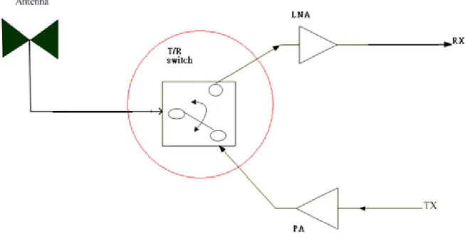
Transmitter (TX)/Receiver (RX) switches have always been a key component of radar and communication systems. It is being an important role between TX and RX port. Fig. 1.1 shows the diagram. RF Switch controls the signal through the low noise amplifier (LNA) or power amplifier (PA) in the T/R module. Therefore, the design of switch is the key performances of the whole transceiver circuit.
Today, most RF switch modules are implemented using GaAs technology, because it has bandwidths of multi-gigahertz and high power handling capabilities. However, the rapid technology evolution of Si MOSFET is beneficial for IC design with higher device speed and cost reduction. Besides the advantages on digital performance, the scaling of CMOS technology has largely improvement along with CMOS technology scaling is the large RF gain, higher cut-off frequency (ft) and maximum oscillation
frequency (fmax). This has made CMOS device technology the prime choice for
Mixed-Signal/RF system-on-chip (SoC) application such as WCDMA, W-LAN, and UWB wireless communication.
Considering the cost down and system integration, high-frequency circuits can be implemented in standard CMOS process. However, the characteristics of low mobility, high substrate conductivity, low breakdown voltage and various parasitic parameters of CMOS processes, it is challenging to design CMOS switches to achieve low insertion loss, high isolation, wide bandwidth and high power handling capability. As CMOS technology is scaled down, the speed improvement furthers the RF performance and makes it suitable for higher frequency applications.
Chapter 2
General Concepts of Switch
2.1 Introduction
RF Switch is an important component in transceiver circuit. Therefore its
performance decides the whole communication system. Because of finite impedance of the switching devices and finite losses of the connecting circuitry, the fabricated switch circuits do not have ideal performance. The following contents describe the RF Switch of insertion loss, isolation and power handling capability.
2.2 Insertion Loss
Switch controls the signal through the transmitter path or receiver path to the Antenna port. The insertion loss of switch will impact the performance of system, it would influences noise figure of receive path directly and data accuracy of transmit path. It is defined as the ratio of the power delivered to the load in the “ON” state of the ideal switch to the actual power delivered by the practical switch, in the ON state. Low insertion loss is importance parameter when we design switch circuit. In the RF circuits, we measure insertion loss with S-parameter and the unit is dB.
2.3 Isolation
Because switch simultaneously connects TX port and RX port, the signal in one port interfere another port is possible. So signal should only transmit signal from TX port to antenna, it would not through switch flow to RX port; in the same way, signal would not through switch flow to TX port if it should receive signal from antenna to RX port. The parameter of judging whether signals influencing other port is called isolation. It is defined as the ratio of the power delivered to the load for an ideal switch in the ON state to the actual power delivered to the load when the switch is in the “OFF” state. In the RF circuits, we measure insertion loss with S-parameter and the unit is dB. The value we hope more higher and higher.
2.4 Power Handling Capability and 1-dB Compression Point
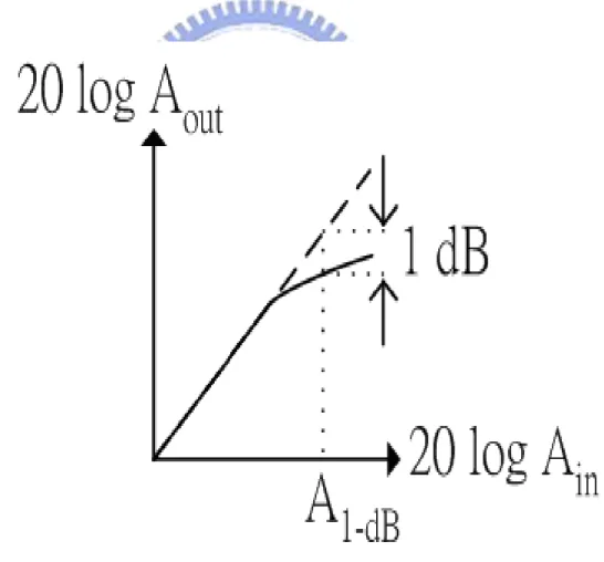
In the transmit mode, signal through switch from PA to antenna, therefore, T/R switch need to handle the great power signal from transmitter in order to avoid signal distortion. In the RF circuits, we measure power handling capability with observing the 1-dB compression point and the unit is dBm. The high P1dB value means high power capability. In RF circuits, “1-dB compression point,"defined as the input signal level that causes the small-signal gain to drop by 1 dB. The output level falls below its ideal value by 1 dB at the 1-dB compression point [1], shown in Fig. 2.1.
When operating within the linear region of a component, gain through that component is constant for a given frequency. As the input signal is increased in power, a point is reached where the power of the signal at the output is not amplified by the same amount as the smaller signal. At the point where the input signal is amplified by an amount 1 dB less than the small signal gain, the 1 dB Compression Point has been reached. A rapid decrease in gain will be experienced after the 1 dB compression point is reached. If the input power is increased to an extreme value, the component will be destroyed.
Chapter 3
Concepts of Switch Circuit Design
3.1 Introduction
With the development of silicon technology, radio frequency circuits can be implemented in standard CMOS process. RF Switch circuit can be one of these circuits with system integration. Therefore, many techniques have been proposed achieve low insertion loss, high isolation and high power handling capability. The following contents describe the methods of how to design a good switch.
3.2 Architecture
There are three basic configurations that may be used for a simple switch designed to control the flow of microwave signals between various ports. These are shown in Fig. 3.1 for a SPDT switch, which consists of series, shunt, and series-shunt configurations. In Fig. 3.1(a), the equivalent circuit model of an on-state transistor is a small resistor. For the off-state transistor, it is represented as a small capacitor. When operating frequency increases, equivalent impedance will become smaller, see eq.3.1. Isolation will become worse between transmit and receive end.
C
j
Z
ω
1
=
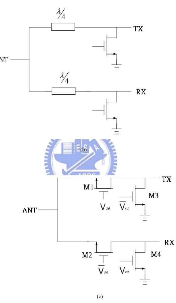
(3.1)In Fig. 3.1(b), the shunt configuration requires a 4λ line in each arm. In a shunt configuration, when a device is in high-impedance state in one arm, the device in the second arm is in low-impedance state. With a 50 ohm 4λ line, the low impedance is transformed to high impedance at the input, while the parallel combination of device’s high impedance and 50 ohm terminal impedance does not affect the input impedance. Thus a 4λ line reduces the effect of device’s low impedance on the input impedance of the switch and keeps the switch circuit matched to 50 ohm at the input under both the ON and OFF states.
(b)
(c)
The schematic of the ordinary switch is shown in Fig. 3.1(c). It is series-shunt type [2]. Transistors M1, M2, M3 and M4 perform the main switch function. A high control voltage turns M1 and M4 on, which enable the path between the antenna and transmitter. Similarly, the receiver path is turned on when the control voltage is low. Two transistors (M1 and M2) in series form a single-pole-double-throw switch. M3 and M4 are two shunt transistors which improve the switch isolation because they provide a way to let signal insert to ground. Therefore, the off path signal will flow to ground and do not interfere the signal of on path.
ctrl
V
The switch is ON when the series device is in the low-impedance state and the shunt device is in the high-impedance state. In the OFF state of the switch, the series device is in the high-impedance state and the shunt device is in the low-impedance state. Isolation obtained with a series-shunt configuration is much better (more than twice in decibels) than that for either series or shunt switch. The insertion loss for the series-shunt configuration is worse than that for a shunt switch but better than that for a series switch. It looks surprising that a switch using two (lossy) devices can have an insertion loss smaller than that with a single device. However, use of a series-shunt switch reduces the reflection loss (compared to that for a series switch) and thereby improves the insertion loss. Using a combination of series-shunt devices eliminates the
The simple equivalent circuit model of an on-state transistor is a small resistor. For the off-state transistor, it is represented as a small capacitor. In this method, we can understand the basic operating state of switch circuit. When operating frequency increases, equivalent impedance will become smaller. From eq. 3.1 we know series-shunt type has the problem that signal loss on off-state path will become worse as frequency increasing. The effect of capacitor coupling is the reasons why insertion loss and isolation performance degraded in high frequency.
3.3 High Power Handling Capability
3.3.1 Introduction
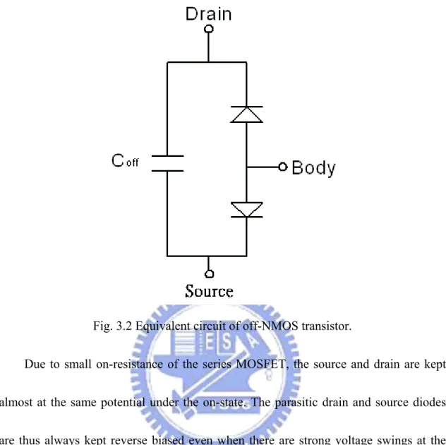
For several communication and radar applications one needs high-power-handling switches. The maximum power handling of switches depends on the maximum voltage that can be applied safely on the device in the OFF state and the maximum current limit of the FET in the ON state. Typical CMOS switches have poor linearity and power handling capability, primarily due to drain and source parasitic diodes. Fig. 3.2 shows the simple equivalent circuit of an off-NMOS transistor.
Fig. 3.2 Equivalent circuit of off-NMOS transistor.
Due to small on-resistance of the series MOSFET, the source and drain are kept almost at the same potential under the on-state. The parasitic drain and source diodes are thus always kept reverse biased even when there are strong voltage swings at the drain and source respectively. Nevertheless, the sources of the shunt MOSFETs are grounded, a negative voltage swing on the drain can push the two back-to-back parasitic diodes into a forward bias region. So the voltage on the drain is clamped to a certain value in the negative region by these forward-biased diodes, leading to distortion in the output signal and then the power handling capability, linearity and insertion loss are degraded. Consequently we know the parasitic diode is the major
3.3.2 Techniques of Improving Power Handling Capability
There are many ways to solve the power-handling capability issue. From the paper [3], it used stacked series transistors to share power, so power-handling capability can be improved. The power handling capacity of FET switches is improved by using FETs having large gate periphery and by stacking N-FETs in series. If the RF swing voltage is evenly divided within the stacked of N-FETs, the power handling capability increases approximately as the square of the number of FETs stacked in a series, and the maximum power is given [19] by
0 2 max 2 )] ( [ Z V V N P = B − p (3.2)
where is the characteristic impedance of the system, and are the gate-drain (or gate-source) breakdown and the pinch-off voltage of the FET, respectively.
0
Z VB Vp
Similarly when the operating voltage ( ) is low and for FETs stacked in a series, the maximum power is given by
c V VB >>Vc 0 2 max )] ( [ 2 Z V V N P = c − p (3.3)
Moreover, the switch uses an LC-tuned substrate biasing technique to dramatically improve the power-handling capability [4]. The body of transistor is series a resonant circuit with capacitance shunt inductance, as shown in Fig. 3.3. It can improve
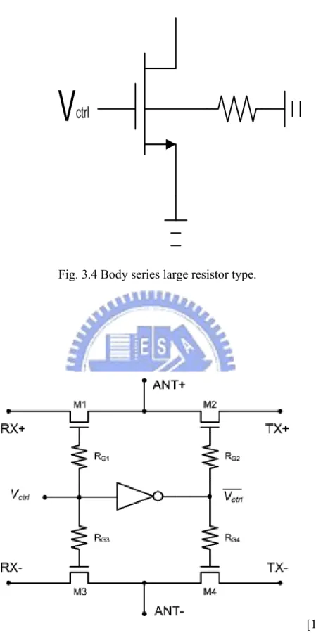
power-handling capability in the specific frequency range. On the other hand, it can be used only on narrow band. Body-floating technique is body series a large resistor about 5kΩ, as shown in Fig.3.4. It has the same operating mode with LC-tuned substrate biasing technique, but it can improve power-handling capability in a wide band. Besides, it can also decrease insertion loss for on-state switch [5] [6]. A 15-GHz T/R switch is reported in [7], the impedance matching network was employed to improve the linearity, while the isolation performance is degraded. The linearity can also be improved by using differential architectures [13] because due to the absence of shunt arm, see Fig. 3.5.
Fig. 3.4 Body series large resistor type.
[13] Fig. 3.5 Architecture of differential T/R switch.
3.3.3 Body-Floating Technique
The goals of T/R switch performance are low insertion loss, high isolation and high power-handling capability.To improve the insertion loss, the substrate resistance RB should be extremely large. If the substrate resistance becomes very large, the path of
signal flowing to ground will become not easy and the loss can reduce. Therefore, it is important to let RB be large enough. Furthermore, the parasitic capacitance associated
with the body will seriously affect the impedance of the switch when the body of the transistor is connected to ground. For these reasons, the body is connected to ground with a large resistor. The large resistor provides an open circuit for the RF signal to improve the insertion loss without affecting the impedance of the switch.
For improve the power performance of the CMOS switch, we can use the body-floating technique [5] [6]. The circuit schematic of a shunt transistor is shown as Fig. 3.6(a). For the off-state NMOS transistor, its simple equivalent circuit is a small capacitance shunt with the two back-to-back parasitic diodes (body to source and body to drain). The equivalent circuit model under off-state is shown in Fig. 3.6(b). In general, body without connecting large resistance and the high input power signal will turn on the diode between body and drain. The diode can be equivalent to a small resistor. A small resistor will cause the current from ground to drain increasing quickly.
power-handling capability as shown in Fig. 3.6(c). If using body-floating technique, the body of the transistor is connected to ground with a large resistor. The high input power signal will still turn on the diode between body and drain. The diode also can be equivalent to a small resistor. But the resistor between body and ground is becoming very large, the current from ground to drain will increase smoothly, see Fig. 3.6(d). For this reason, power-handling capability can be improved by using body-floating technique.
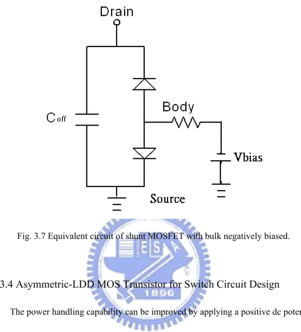
In fact, the technique that body floated and negatively biased simultaneously can have better result about increasing the switch’s linearity and power handling capability [16], see Fig. 3.7. It shows the floating body of the shunt MOSFET is biased using a negative dc voltage via the body bias resistor. Since there is no current flow through large body resistor, the dc potential of the bulk node is kept the same as the negative bias. Therefore, the source parasitic diode is always in the reverse bias and the drain parasitic diode can bear a strong negative voltage which larger than ordinary body floating circuit. So using the negative body bias technique can lead to a larger power handling for T/R switch.
(a) (b)
(c) (d)
Fig. 3.7 Equivalent circuit of shunt MOSFET with bulk negatively biased.
3.3.4 Asymmetric-LDD MOS Transistor for Switch Circuit Design
The power handling capability can be improved by applying a positive dc potential to the drain of the shunt MOSFET [16]. This technique is useful when the RF signal entering the RX or leaving the TX port has a positive dc offset.
The rapid technology evolution of Si MOSFET is beneficial for IC design with higher device speed and cost reduction. However, the low drain breakdown voltage of CMOS transistors limits the use of CMOS for power amplifiers. This limitation for high voltage operation significantly reduces the maximum output power and efficiency for CMOS devices. To overcome the low breakdown voltage issue and improve the RF
power performance, we use asymmetric-lightly-doped-drain (LDD) MOS transistor for high frequency RF power application [11].
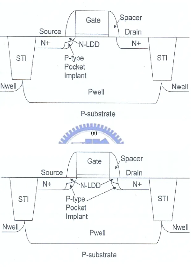
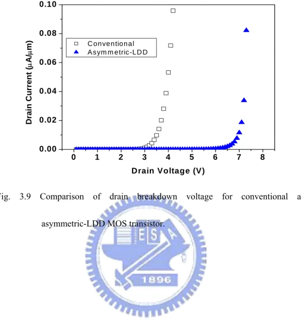
This new asymmetric MOSFET is fully embedded in the conventional foundry logic process without any additional process step or extra cost. The asymmetric-LDD MOS transistor has higher drain breakdown voltage. The structure comparison of (a) the new asymmetric-LDD MOS transistor and (b) conventional MOS transistor are shown schematically in Fig. 3.8. The LDD region at the drain size was removed that is the major difference to conventional MOS. This large improvement of breakdown voltage is due to the designed wide depletion region beneath the spacer region and between the drain and substrate. Such wide depletion region in the new design can support significantly larger reverse-biased drain voltage than conventional case. Figure 3.9 shows the comparison of DC drain breakdown voltage for conventional and asymmetric-LDD MOS transistor. For conventional MOS, the breakdown voltage is 3.5V. In sharp contrast, the breakdown voltage of asymmetric-LDD MOS is increased to 6.9V. So we can use the asymmetric-LDD MOS in our switch design to improve power-handling capability because we could apply higher dc voltage to the drain of the shunt MOSFET.
(a)
(b)
Fig. 3.8 Device structures of (a) an asymmetric-LDD MOS transistor and (b) a conventional MOS transistor.
0 1 2 3 4 5 6 7 8 0.00 0.02 0.04 0.06 0.08 0.10 Drain Current ( μ A/ μ m) Drain Voltage (V) C onven tional A sym m etric-LD D
Fig. 3.9 Comparison of drain breakdown voltage for conventional and asymmetric-LDD MOS transistor.
Chapter 4
T/R Switch Circuit
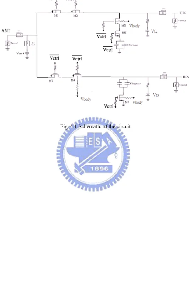
4.1 Circuit Topology
Fig. 4.1 shows the circuit schematic. This circuit was designed with Agilent Advanced Design System (ADS), and implemented in TSMC 0.18μm RF CMOS technology. Due to the different requirements in the TX mode and the RX mode, the switch is designed to be asymmetric. The T/R switch was designed by series-shunt topology using body-floating technique and asymmetric-LDD MOS transistor.
The devices of M1、M2、M3、M4 are the series transistors, and M5、M6、M7 are the shunt transistors which can improve the isolation of T/R switch. The signal is transmitted from TX node to ANT node and received from ANT node to TX node. Cbypass is on-chip bypass capacitor which provides ideal ac ground. It can isolate DC to
avoid DC power consumption. The on-state and off-state of transistors are shown as Table 4.1. On-state transistor is biased at 1.8V and off-state transistor is biased at 0V. M5 use asymmetric-lightly-doped-drain (LDD) MOS which is our LAB developed MOS. This large improvement of breakdown voltage is due to the designed wide depletion region beneath the spacer region and between the drain and substrate. Asymmetric-LDD MOS transistor can endure high voltage. The key point is the large bias region on the transmitter path to improve the power linearity. Therefore, the higher
drain breakdown voltage of asymmetric-LDD MOS transistor is used for the transmitter path. In this circuit, TX node is biased at 3.5V more than 1.8V in conventional MOS transistor. It can increase voltage swing, therefore improving the power-handling capability of T/R switch. Besides, the transistors M4、M5、M7 use the body-floating technique. The body-floating technique is to keep the parasitic diodes from being forward bias under large input signals, hence, improving the linearity and power-handling capability of CMOS T/R switch. In shunt path of TX port, the transistor M6 series with M5 and Cbypass. In series path, utilize stacked transistor
configuration to improve the power-handling capability. But it will also make the insertion loss increasing on the transistor-on mode.
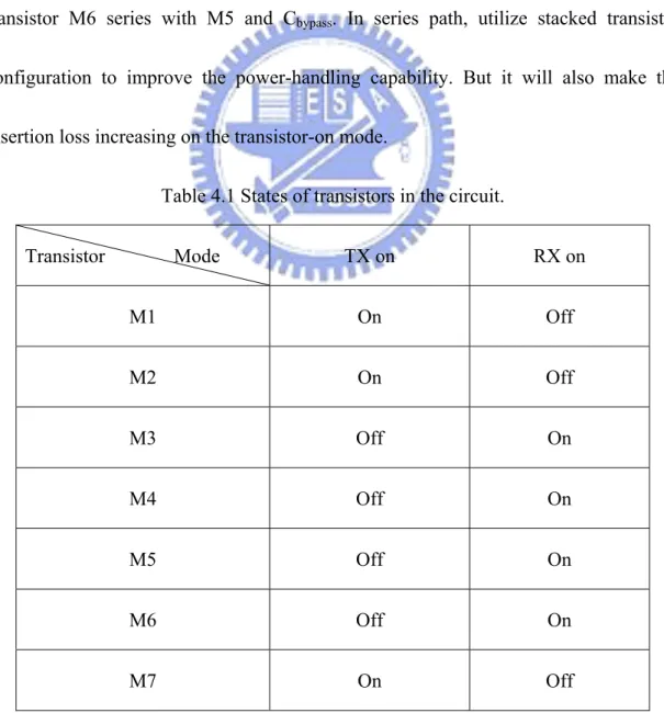
Table 4.1 States of transistors in the circuit.
Transistor Mode TX on RX on M1 On Off M2 On Off M3 Off On M4 Off On M5 Off On M6 Off On
4.2 Simulation and Measurement Result
The RF performance of the UWB CMOS T/R switch has been measured by using network analyzer and on-wafer probing system. The control voltage is 1.8V for on-state and 0V for off-state in small signal measurement. In large signal measurement, due to TX node and ANT node bias 3.5V, the control voltage in TX port becomes 5.3V.
4.2.1 TX Mode
The signal from antenna to transmit mode is TX mode. Figure 4.2 shows the simulated and measured insertion loss of the SPDT switch under TX mode and Fig.4.3 show isolation. The power-handling capability shows in Fig 4.4. Within 3.1-10.6GHz, the CMOS T/R switch exhibits insertion loss of less than 2.5 dB and isolation between 29.8 to 31.7 dB. The measured 1-dB power compression point is 24.5 dBm.
Fig. 4.2 Simulated (upper line) and measured (lower line) insertion loss under TX-on.
Fig. 4.4 Measured P1dB under the TX mode.
4.2.2 RX Mode
The signal from antenna to receive mode is RX mode. Fig. 4.5 shows the simulated and measured insertion loss of the SPDT switch under RX mode and Fig. 4.6 shows isolation. Within 3.1-10.6GHz, the receive mode exhibits insertion loss of less than 3.5 dB and isolation between 25.0 to 31.5 dB. The layout is shown in Fig. 4.7 and the die is shown in Fig. 4.8. Its area is 550μm×495μm.
Fig. 4.5 Simulated (upper line) and measured (lower line) insertion loss under RX-on.
4.3 Summary
By the series-shunt structure, techniques which includes asymmetric-LDD MOS transistor, body-floating and high voltage apply on TX port. Table 4.2 is the comparison of T/R switch performance. It shows acceptable result about power-handling capability by using asymmetric-LDD MOS transistor in this table. In this table, some designers do not use shunt path of TX port, so their power handling capability are very high. If the condition is the same (each one has no shunt path of TX), this circuit performs be slightly superior to others in power handling capability. Otherwise, because this circuit did not use inductor, the die area is not large comparing with others. However, the disadvantage of this circuit is the higher insertion loss on RX mode. In the chapter5, the issues and improvement methods will be discussed.
Table 4.2 Comparisons of T/R switch performances. *Effective chip area Referenc e Process Frequency (GHz)
Loss(dB) Isolation (dB) P1dB(dBm) Technology Chip area(mm2)
TX 1.5 TX 30 [12] 0.18um CMOS 5.2 RX 1.4 RX 15 28 Narrow band,LC-tuned Substrate Bias 0.56 0~10 0.5-0.7 >32 25.4-26.2 10~18 0.7-1.0 25-32 22.6-25.4 [16] 0.18um CMOS 18-20 1.0-2.5 25 19.8-22.6 Bias and Pattern Ground Shield Inductor 0.06* [5] 0.18um CMOS 5.8 1.1 27 20 Body-Floating 0.03* 0~10 0.9-1.7 >32 10~15 1.7 32 [17] 0.13um CMOS 20 1.7-2.0 21 30 Differential &Bias& Customized nMOS 0.17/0.027* 10 1.3 23 15 1.9 22 [13] 0.13um CMOS 20 2.0 21 25.5 Switched body floating& Customized nMOS 0.015 TX <2.56 TX >29.8 This work 0.18um CMOS 3.1~10.6 RX <3.53 RX >25.0 24.5 Asymmetry MOS 0.27
Chapter 5
Discussions and Improvements
5.1 Analyzing Power Handling Capability
5.1.1 Different Bias in P1dB Measurement
When applying different voltage on TX port, ANT port and body, the measured P1dB data are different. Table 5.1 shows the result.
Table 5.1 P1dB of different bias.
condition Vctrl Vbody Vtx Vant P1dB
I 1.8 0 0 0 16.85 II 3.6 0 1.8 0 17.85 III 3.6 -1.8 1.8 0 20.85 IV 3.6 0 1.8 1.8 22.85 V 3.6 -1.8 1.8 1.8 24 VI 5.3 -3.5 1.8 1.8 24.5
Comparing with condition I and II, the P1dB is improved by bias voltage comparing to condition III and IV. In condition IV、V、VI, the ANT port is also bias positive voltage. This concept is proposed in [8]-[10]. The TX and ANT node voltage reverse bias the
drain/ source to substrate p-n junction, therefore, improving the power handling capability. Condition VI is the optimized P1dB result.
5.1.2 The Issue of Power Handling Capability
In order to find out the issue of degraded power handling capability, laser cutting is been used. There are three types laser cutting die. First is cutting the shunt circuit of TX path (the node 1 in Fig. 5.1). Second is cutting receiver path (the node 2 in Fig. 5.1) and last is cutting the shunt circuit of TX path and RX path (the node 1 and 2 in Fig. 5.1). The measured data is in Table 5.2 and table 5.3. In table 5.2, the bias condition is the V of table 5.1. In table 5.3, the bias condition is the VI of table 5.1. In shunt circuit of TX path, the power degradation is about 6 dB. In RX path, the power degradation is about 4 dB. If both RX path and shunt circuit of TX path are cutting, the P1dB can improved to 35~36 dBm. From these results can know the off state of transistor is the key reason degrades the power handling capability.
Table 5.2 Measured P1dB of condition V
Die condition P1dB (dBm)
Complete die 24
Cut position 1 29.85
Table 5.3 Measured P1dB of condition VI.
Die condition P1dB (dBm)
Complete die 24.5
Cut position 1 30.85
Cut position 2 28
Cut position 1 & 2 36
5.2 The Improvement of Power Handling Capability
5.2.1 The Equivalent Capacitor Cds
From the section 5.1.2, the equivalent capacitors of switch circuit are the issue of degraded insertion loss as well as power handling capability. For this reason, reducing capacitor value is the immediate thought and then the equivalent impedance become large. In equation 5.1, the parallel-plate capacitor:
d
A
C
=
ε
(5.1)Where ε is permittivity, A is plate area and d is the distance between parallel plates. From this equation, enlarging distance of the parallel plates is the method of reducing capacitor value. Therefore, Fig. 5.2 shows the conventional and customized transistor layout. The customized transistor layout is enlarging the distance between source and drain, so the capacitor is reduced and then the goal of increased equivalent impedance is reached.
If the equivalent impedance of capacitors becomes higher, it means the effect of closing path is more effective. So the signal will not couple through the off-transistor and then the loss is reduced.
discussed in section 3.3.1. But except for body have parasitic diode, the deep n-well also have. A deep n-well (DNW) is offered as default in the TSMC 0.18μm mixed-signal process for better substrate isolation with an additional p-n junction. Therefore, the additional DNW bias is also needed. Fig 5.3 shows the cross-sectional view of NMOS. From this figure there are parasitic diodes between DNW and p-type substrate, p-type body and DNW. Due to these parasitic diodes, the power handling capability is degraded. So connecting large resistor to DNW node could improve the power handling capability. If apply positive voltage in DNW node, the improving effect will become better. Because the positive voltage can reverse bias the diodes and large resistor can let current flow smoothly, the power handling capability consequently improved. Therefore, apply large resistor in DNW node is effective in improve power handling capability.
(a)
(b)
Chapter 6
Conclusion
This paper demonstrates a CMOS T/R switch designed for ultra wideband and higher frequency applications. The LDD MOSFET has been used in this circuit to increase voltage bias on TX node and then improving the power handling capability. The switch achieves 2.5 dB and 3.5 dB in TX and RX mode under 10.6 GHz, and isolation of 29.8-31.7, 25-31.5 dB, respectively. The measured 1-dB power compression point is 24.5 dBm. The power performance is also analyzed by laser cut. The newly designed switch will be improved the insertion loss and power capability by smaller parasitic capacitor and control diode voltage method.
Reference
[1] B. Razavi, “RF Microelectronics,” 1st ed. NJ, USA: Prentice-Hall PTR, 1998.
[2] Hieda M., Nakahara K., Miyaguchi K., Kurusu H., Iyama Y., Takagi T., and Urasaki S., “High-isolation series-shunt FET SPDT switch with a capacitor canceling FET parasitic inductance,"IEEE Transaction on Microwave Theory and
Techniques, vol. 49, no. 12, December 2001, pp. 2453-2458.
[3] Ohnakado T., Yamakawa S., Murakami T., Furukawa A., Taniguchi F., Ueda H. Suematsu N., and Oomori T., “21.5-dBm power-handling 5-GHz transmit/receive CMOS switch realized by voltage division effect of stacked transistor configuration with depletion-layer- extended transistors (DETs),"IEEE Journal of Solid-State
Circuits, vol. 39, no. 4, April 2004, pp. 577-584.
[4] Niranjan A. Talwalkar, C. Patrick Yue, Haitao Gan, and S. Simon Wong, “Integrated CMOS transmit-receive switch using LC-tuned substrate bias for 2.4-GHz and 5.2-GHz applications,"IEEE Journal of Solid –State Circuits, vol. 39, no. 6, June 2004, pp. 863-870.
[5] Mei-Chao Yeh, Ren-Chieh Liu, Zuo-Min Tsai and Huei Wang, “A miniature low-insertion-loss, high-power CMOS SPDT switch using floating-body technique for 2.4-and 5.8-GHz applications," IEEE Radio Frequency Integrated Circuits
[6] Mei-Chao Yeh, Zuo-Min Tsai, Ren-Chieh Liu, Kun-You Lin, Ying-Tang Chang, and Huei Wang, “Design and analysis for a miniature CMOS SPDT switch using body-floating technique to improve power performance, " IEEE
Transactions on Microwave Theory and Techniques, vol. 54, no. 1, Jan. 2006, pp.
31-39.
[7] Zhenbiao Li and Kenneth K. O, “15-GHz fully integrated nMOS switches in a 0.13um CMOS process,” IEEE J. Solid-State Circuits, vol. 40, no. 1, Nov. 2005, pp.2323-2328
[8] F. J. Huang and K. K. O, “A 900-MHz T/R switch with a 0.8-dB insertion loss implemented in a 0.5-um CMOS process,” in Proc. IEEE Custom Integrated
Circuits Conf. (CICC), May 2000, pp. 341-344
[9] Feng-Jung Huang and Kenneth O, “A 2.4-GHz single-pole double-throw T/R switch with 0.8-dB insertion loss implemented in a CMOS process,” in Proc. Eur.
Solid-State Circuits Conf. (ESSCIRC), Sep. 2001, pp.432-435
[10] Z. Li, H. Yoon, F. J. Huang, and K. K. O, “5.8-GHz CMOS T/R switches with high and low substrate resistances in a 0.18-um CMOS process,” IEEE Microwave
Wireless Compon. Lett., vol. 13, no. 1, pp. 1-3, Jan. 2003
and Wireless Components Letters, vol. 17, no. 6, June 2007, pp. 445-447
[12] N. Talwalkar, C. Yue, and S. Wong, “An integrated 5.2GHz CMOS T/R switch with LC-tuned substrate bias,” IEEE Int. Solid-State Circuit Conf. (ISSCC) Dig.
Tech. Papers, Feb. 2003, pp.362-363
[13] Y. P. Zhang, Qiang Li, Wei Fan, Chew Hoe Ang, and He Li, “A Differential CMOS T/R Switch for Multi-standard Applications,” IEEE Transactions on
Circuits and Systems, vol. 53, no. 8, Aug. 2006, pp.782-786
[14] Feng-jung Huang and Kenneth K. O,“Single-pole double-throw CMOS switches for 900-MHz and 2.4-GHz applications on p-silicon substrates, " IEEE J.
Solid-State Circuits, vol. 39, no. 1, Jan. 2004, pp. 35-41,
[15] K.-H Pao, C.-Y. Hsu, H.-R. Chuang, C.-L Lu and C.-Y Chen, “A 3-10GHz Broadband CMOS T/R Switch for UWB Applications”, 1st European Microwave
Integrated Circuits Conference, September 2006, Manchester, Uk, pp.452-455,
[16] Yalin Jin and Cam Nguyen, “Ultra-compact high-linearity high-power fully integrated DC-20-GHz 0.18μm CMOS T/R switch, ”IEEE Transactions on
Microwave Theory and Techniques, vol. 55, no.1, Jan. 2007, pp. 30-36
[17] Q. Li and Y. P. Zhang, “CMOS T/R Switch Design: Towards Ultra-Wideband and High Frequency,” IEEE J. Solid-State Circuits, vol. 42, no. 3, Mar. 2007, pp.563-570
[18] Y. C. Wu, E. Y. Chang, Y. C. Lin ,H. T. Hsu, S. H. Chen, W. C. Chen, W. C. Wu, L. H. Chu, and C. Y. Chang,“SPDT GaAs switches with copper metallized interconnects,"IEEE Microwave and Wireless Components Letters, vol. 17, no.2, Feb. 2007, pp. 133.135.
[19]Kai Chang, Inder Bahl, Vijay Nair, “RF and Microwave Circuit and Component Design for Wireless Systems,” 1st ed. NY, USA, Wiley- Interscience. 2002