Efficient techniques in the sizing and constrained
optimisation of CMOS combinational logic circuits
J.-S. Hwang c.-Y. wu
Indexing terms: Optimisotion, Logic
Abstract: Two techniques are proposed which enhance the optimisation efficiency of CMOS combinational logic circuits. One uses transition times (rise and fall times) of each gate as variables of the optimisation process. The other technique uses the optimal characteristic waveform synthe- sising method (OCWSM) to obtain the initial guess for the optimisation process. The opti- misation process, with these two techniques, can perform sizing and optimisation for circuits with a smaller fixed-delay specification than other sizing and optimisation algorithms. The circuits sized using the proposed algorithm have shown a smaller power dissipation, especially when the delay specification is small. The CPU time con- sumed is reasonable. High-speed low-power cir- cuits are thus more realisable using the proposed algorithm.
List of symbols
Cbd,n,,l = drain-bulk junction capacitance of
PMOSFET(NM0SFET) in CMOS inverter, estimated at output voltage V , = (V,,
C,,,,,,, = drain-bulk junction capacitance of
PMOSFET(NM0SFET) in CMOS inverter, estimated at output voltage V , = VD/DsATN/2 Cbdp(n,rl = drain-bulk junction capacitance of
PMOSFET(NM0SFET) in CMOS inverter, estimated at output voltage V , = (V,,
- V D S A T P ) / ~
Cbdp(n,,2 = drain-bulk junction capacitance of
PMOSFET(NM0SFET) in CMOS inverter, estimated at output voltage V , = (V,,
C,,,(,,,, = gate-drain overlap capacitance of
PMOSFET(NM0SFET) in CMOS inverter, estimated when output voltage V , lowers from VDD to Vg,,,, and NMOSFET is oper- ated in saturation region
C,,,,(,,,, = gate-drain overlap capacitance of
PMOSFET(NM0SFET) in CMOS inverter, estimated when output voltage V , lowers from V,,,,, to 0 V and NMOSFET is oper- ated in linear region
+ vDSATN)/2
+ vDSATP)/2
Paper 7946E (C2, ElO), first received 18th June and in revised form 12th November 1990
The authors are with the Department of Electronic Engineering, National Chiao Tung University, 75 Po-Ai Street, Hsin-Chu, Taiwan 30039, Republic of China
154
-
r
-Cgdp(n,rl = gate-drain overlap capacitance of
PMOSFET(NM0SFET) in CMOS inverter, estimated when output voltage V , raises from 0 V to V,,-V,,,,, and PMOSFET is operated in saturation region
Cgd,n,,2 = gate-drain overlap capacitance of
PMOSFET(NM0SFET) in CMOS inverter, estimated when output voltage
V ,
raises from V,,-V,,,,, to V,, and PMOSFET is operated in linear regionCssp(n,,l = gate-source overlap capacitance of PMOSFET(NM0SFET) in CMOS inverter, estimated when output voltage
V ,
lowers from V,, to V,,,,, and NMOSFET is oper- ated in saturation regionC,,,(,,,, = gate-source overlap capacitance of PMOSFET(NM0SFET) in CMOS inverter, estimated when output voltage V , lowers from V,,,,, to 0 V and NMOSFET is oper- ated in linear region
Cssp,n,,l = gate-source overlap capacitance of PMOSFET(NM0SFET) in CMOS inverter, estimated when output voltage V , raises from O V to VDD- VDSATP and PMOSFET is operated in saturation region
Cgsp(n)rZ = gate-source overlap capacitance of PMOSFET(NM0SFET) in CMOS inverter, estimated when output voltage V , raises from VDD-VDSA,, to V,, and PMOSFET is operated in linear region
CL = output capacitive loads
G A M M A = bulk threshold parameter (SPICE device
parameter)
= effective channel length of
PMOSFET(NM0SFET)
= equivalent fall pole of input waveform defined as P f i = (In 2)/TFi
=equivalent rise pole of input waveform defined as P,i = (In 2)/TRi
= fall time which is time interval within which output voltage lowers from 0.9 V'D to 0.1
v,,
= fall time which is time interval within which input voltage lowers from 0.9 VDD to 0.3 V D ,
= fall delay time which is time interval between input voltage = 0.5 V,, and output voltage V , = 0.5 V D D
= rise delay time which is time interval between input voltage = 0.5 V,, and output voltage
V ,
= 5 V,,= rise time which is time interval within which output voltage raises from 0.1 V,, to 0.9 VDD
= rise time which is time interval within which input voltage raises from 0.1 V,, to 0.9 V,,
= channel oxide thickness
= velocity saturation voltage of NMOSFET = velocity saturation voltage of PMOSFET = final threshold voltage of a-channel
MOSFET under the condition that gate voltage V, = V,, and source voltage Vs =
VTNF
= zero-bias threshold voltage of
MOSFET(SP1CE device parameter)
= channel width of a@)-channel MOSFET = permittivity of Si semiconductor (silicon
= effective channel length modulation param-
= n(p)-channel parameter 7
= effective short-channel N(P)MOSFET
= Fermi potential
= Fermi potential of n(p)-type silicon
= surface mobility of carriers = effective n(p)-channel ps
dioxide)
eter (SPICE device parameter)
GAMMA
1 Introduction
Sizing the transistors of a CMOS digital IC when opti- mising various circuit performance parameters such as delay time, power dissipation and chip area has been an important and challenging area of work. There have been many publications [l-141 which have discussed sizing and optimisation algorithms for MOS logic circuits. Some consider the transistor sizing along the critical delay path (the selected path) only [3-9, 11, 123. This lacks a global view of the whole circuit. Others [I, 2, 10,
131 apply mathematical optimisation techniques to solve the transistor sizing problem. The design object is formu- lated as a nonlinear mathematical equation, with the desired specifications as constraints, and then optimised through a timing analyser [IO, 131 or a circuit simulator [I, 23. For the sizing and optimisation using general- purpose circuit simulators [I, 21, the manageable circuits are typically restricted to those with at most thirty design parameters [IO]. For the sizing and optimisation using timing analysers, no such restrictions exist.
In all the sizing and optimisation algorithms proposed [l-141, the device sizes have been chosen as independent variables of the optimisation process because they are the desired solution. Since the relation between delay time and device sizes is very complex, the efficiency in the optimisation using device sizes as optimisation variables may be degraded. The initial guess (initial device sizes) of the optimisation process are either arbitrarily chosen by the user
[lo]
or obtained from the heuristic approach [13]. The required circuit performance is usually different from that achieved when using the user-assigned device sizes (usually the minimum allowable device sizes). This may cause difficulties in the optimisation process because large iteration number and large CPU time consumption may result. The convergence speed can be greatly enhanced by using the heuristic approach to obtain the initial guess for the optimisation process. As the specified delay time approaches the optimal value, the required CPU time in the heuristic approach is intolerable even for a medium-size circuit [13].This paper aims to solve the above mentioned prob- lems. Two techniques in sizing CMOS combinational
IEE PROCEEDINGS-E, Vol. 138, No. 3, MAY 1991
logic circuits are proposed. The output transition times (rise and fall times) of each gate, instead of the device sizes, are chosen as independent variables of the opti- misation process. The optimised transition times are then used to calculate the required device sizes using the physical timing models [l5-181. The initial guess of tran- sition times in the optimisation process is obtained from a simple and quick pre-optimiser which uses the optimal characteristic waveform-synthesising method (OCWSM) [19, 201 to obtain near optimal transition times with much less CPU time.
These two techniques are applied to the minimisation of power dissipation with fixed-delay specifications for the sizing of CMOS combinational logic circuits. Many optimisation methods [21, 231 can solve this constrained optimisation problem. Minimising the augmented Lagrangian function of the equality constrained problem combines the advantages of the penalty and the primal- dual approaches [21]. It is therefore adopted in the mini- misation of power dissipation with fixed-delay specifications. The Davidon-Fletcher-Powell method [21, 231 is an optimisation method with quadratic con- vergence rates. This method uses only the functional values and gradient vectors in generating mutually conju- gate search directions. It is very suitable for the sizing of CMOS combinational logic circuits from the computa- tion point of view. However, the optimisation result may converge to a nonoptimal point because of the round-off errors, numerical errors, inaccurate line searches and nonquadratic terms in the objective function [23]. The self-scaling and restarting quasi-Newton method [23] is thus adopted in solving the above mentioned opti- misation problem.
The adopted timing models must be accurate when using timing analysers for the sizing and optimisation. Otherwise, the results of sizing, optimisation, and timing verification would have an unbearable error. Many timing models [4, 11, 12, 15-18, 24-32] and timing simu- lators [33] have been developed. The physical timing models developed by the present authors [lS-lS] show a satisfactory accuracy for CMOS combinational gates with wide ranges of device sizes, capacitive loads, device parameter variations and input excitation waveforms. Although the models have complicated equations of gate delay times as a function of device parameters, the required CPU time is still much smaller than that in con- ventional circuit simulators.
The physical timing models of CMOS static logic gates are described. The power dissipation model of CMOS static logic gates are given. The details of the pro- posed techniques are given and some experimental results to verify the proposed techniques presented. Finally, con- clusions and discussions are given.
2 Physical timing models of CMOS combinational gates
The timing models [lS-lS] adopted in the sizing and optimisation process are developed by deriving, region by region, the analytical formulas of the rise/fall times ( TR/TF) from the linearised large-signal equivalent circuit of a CMOS logic gate, under the characteristic-waveform consideration. Tables 1 and 2 list the expressions of rise and fall times for short-channel CMOS inverters, respec- tively. The rise and fall delay times TPLH and TPHL are semi-empirically expressed in terms of the calculated rise/ 155
fall times as where ar,, a , J l a/,, and aJJ are universal empirical con- In 2 In 2 stants for the initial delay. The above equations are uni- TpLH = a,, TR
+
a,J TFi+
-
In 9 TR - - In 9 TFi versa1 for different device and circuit parameters of the logic gate. Applying this modelling technique, timing In 2 In 2 (2) models have been derived for CMOS inverters [lS, 171, multi-input NAND and NOR gates [lS, 171, A01 and In 9 In 9 ‘ ~ i( l ) TPHL = Q J ~ TR;
+
a J J TF+
-
TF - -Table 1 : Rise t i m e equations for short-channel C M O S inverters
Table 2: Fall time eauations for short-channel C M O S inverters
156
(
(V,, + 1/A,F1 = V,, exp ( - 0 . 6 )
OAI gates [18], and static flip-flops [16] with MOS device channel length (mask) down to 1.5pm.
The accuracy of the timing models has been widely verified through extensive comparisons between model calculation and SPICE simulation. Part of the compari- sons are shown in Fig. 1 for 2 pm CMOS inverters with C, = 0 pf (only one fanout) under characteristic- waveform consideration. Fig. 2 shows the comparisons of 2 pm CMOS inverters with C, = 0 pf (only one fanout) under the exponential input excitations with time con- stants from 0.4 to 4.0 ns. It is found through the accu- racy verification that the maximum error is under 15% for inverters with different device dimensions, capacitive loads, input waveforms, device parameters and tem- peratures. Fine tuning can further decrease the error to below 7% [17].
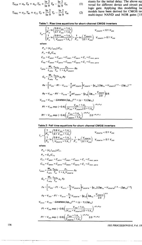
The timing models should be able to characterise the timing of multi-input logic gates excited at any input node to accurately calculate the delay time of a logic circuit. A CMOS three-input NAND gate, as shown in
4 8 16 32 64 128
channel width ratio Fig. 1
2.0 pm CMOS inverters
Charactenstic waveform consideration C, = OpF; W, = W,; L,,,dL,,,, =
-0- SPICE risc delay - - - - theory rise delay
-T- SPICE fall delay -A- theory fall delay
Rise and fall delays against channel width ratio
0.911.1 p 2 O r L
:
i
j
1 4 In 1 2 t 0 1 " ' . , . . . , , 0 2 0 4 0 7 0 9 1 1 1 3 16 18 2 0time contant of exponential input.ns Fig. 2
2.0 pm CMOS inverters Exponential input excitations
C , = OpF; W, = W, = 2 p m
+
SPICE rise delay - - 0 - - theory rise delay --Ef SPICE fall delay - - -- theory fail delayIEE PROCEEDINGS-E, Vol. 138, N o . 3, M A Y 1991 Rise and fall delays against time constants
Fig. 3, is considered. The timing is of the worst-case type if only the input node 1 is excited. The other inputs nodes are stabilised at V',. If the node 2 or the node 3 is
Vnn Mpl Mp2 Mp3
n
I I v - I I
driver stage load stage Fig. 3
Triggering at node 2
CMOS three input N A N D gate
excited and the other nodes are stabilised at V,,, the timing is not the worst case type. According to our obser- vations, the longest rise delay of a CMOS three-input NAND gate with one fanout gate is about 58% longer than the corresponding shortest one. The timing models [l5, 181 developed by the authors considered all the trig- gering cases. Part of the comparisons between the SPICE simulation and the model calculation are listed in Table 3 for 2pm CMOS three-input NAND gates in different triggering cases. It is shown through the accuracy verifi- cation that the maximum error of the developed timing models is under 15% for CMOS multi-input NAND/ NOR gates with wide ranges of device sizes, capacitive loads and device parameter variations. The input voltage waveforms were not deviating much from characteristic waveforms. Fine tuning can further reduce the maximum error to below 10% [17].
Table 3: Signal timing of 2.0" CMOS three input NAND gates
Triggered Signal SPICE Theory Error
node timing ns ns % 3. Rise time 1.407 1.469 4.4 Fall time 1.553 1.454 -6.4 Rise-delay 0.812 0.736 -9.3 Fall-delay 0.800 0.745 -6.8 2 Rise time 1.792 1.939 8.2 Fall time 1.593 1.647 3.4 Rise-delay 1.099 1.020 -7.2 Fall-delay 1.01 9 0.979 -3.9 I t Rise time 2.182 2.456 12.6 Fall time 1.568 1.728 10.2 Rise-delay 1.288 1.315 2.1 Fall-delay 1.1 70 1.01 5 -1 3.2 W p = 2 . 0 p m ; W,,=2.0pm;CL=OpF * Node nearest output node
t Node furthest from output
A similar error characteristic can be obtained for the timing models of small-geometry CMOS AOI/OAI gates C181.
3 General power dissipation models of CMOS combinational gates
Consider a string of CMOS three-input NAND gates excited at the node 2 as shown in Fig. 3. Typical output voltage characteristic waveforms of
v2,
V , , V,, and V,, are shown in Fig. 4. As the input voltageK 2
rises from 0 V to V,,, the output voltages V , andV,,
fall from V,, to 0 V and (V,, - V,,,) to 0 V, respectively. V,,, is thethreshold voltage of an n-channel MOSFET with the source-bulk voltage V,, = V,, - V,,,. The output voltage V,, first raises from 0 V to V, and then falls from
v,
to 0v.
6 - cn 120 180 2LO 300 time,ns Fig. 4 Triggering at node 2 C , = 5.0 pFTypical fall characteristic of CMOS three input N A N D gate
To neglect the short-circuit power dissipation is an acceptable approximation as long as the short-circuit power dissipation is small compared with the dynamic power dissipation needed to charge the capacitor [l 11. According to our observations, the energy loss of a CMOS logic circuit is mainly caused by the charging and discharging of device capacitances during the output rising/falling transition periods when the CMOS logic circuits are operated under the characteristic-waveform consideration. Only the dynamic power dissipation is considered.
There are four different types of device capacitances: voltage-dependent drain (source)-bulk junction capac- itance, voltage-dependent gate-drain (source, bulk) capac- itance, voltage-independent gate-drain (source) overlap capacitance, and external voltage-independent capac- itances. The energy loss during the charging/discharging cycle of a capacitor is equal to the change of the energy stored on the capacitor [34]. To characterise the change of the energy stored on the voltage-dependent pn junc- tion capacitances, the case of the drain-bulk junction capacitance is considered. The change of stored energy from the drain-bulk voltage V,, = 0 V to V,, =
Gias
is derived in the Appendix. For CMOS three-input NAND gates excited at the node 2, the change of the energy stored on voltage-dependent drain-bulk junction capac- itances can be further divided into three subgroups.(a) Drain-bulk junction capacitances at the output node: In a typical CMOS logic gate, the substrate of the PMOS is connected to the positive power supply V,,. When the output voltage is V,,, the voltage across the drain-bulk junction capacitance of the PMOSFET is 0 V. There is no charge stored on this capacitor. The voltage across this capacitance is V,, when the output voltage is OV. The change of the energy during each transition period can then be expressed as
b p = CJp A D , p Fa,,,, ,CVDD)
+ CJSWpf',, p F p e r i . ~ ( V D D ) (3) where CJ, is the zero-bias bulk capacitance of the PMOSFET, C J S W , is the zero-bias perimeter capac- itance of the PMOSFET, A , , , is the drain area of the 158
PMOSFET, is the drain perimeter of the
PMOSFET, F,,,, p( V,,) and F,e,i, p( V,,) can be found from the Appendix for the PMOSFET.
The change of the energy stored on the drain-bulk junction capacitance of the NMOSFET can be also expressed by using the same derivation technique.
(b) Drain-bulk junction capacitances of internal series NMOSFETs: The voltage swing of V,, at the node 3 is
V,, VTNF. Thus, the change of the energy on the drain-
bulk junction capacitor at this node is 8" = CJ, AD, Fare,, AVDD - VTNF)
(4) where CJ, is the zero-bias bulk capacitance of the NMOSFET, CJS W, is the zero-bias perimeter capac- itance of the NMOSFET, A,," is the drain area of the NMOSFET, P,," is the drain perimeter of the NMOSFET, Farea, - V,,,) and F p e r i , AV,, - VTNF) can be found from the Appendix for the NMOSFET.
( e ) Internal inactive drain-bulk junction capacitances: From Fig. 4, it is found that the voltage at the node 2
(K,)
before the transition period is 0 V, so is the voltage after the transition period. The bias voltagehias
is 0 V. From the Appendix, the change of the energy on such an inactive drain-bulk junction capacitor is 0, as is the power dissipation.The change of the energy stored on the voltage- dependent source-bulk junction capacitor can also be for- mulated. For the voltage-dependent gate-drain (source, bulk) capacitance, its energy change is calculated region by region with suitable capacitance values determined by the device operating regions. For the voltage-independent gate-drain (source) overlap capacitance and external voltage-independent capacitances, the energy change can be easily characterised. The total energy loss during the rising/falling transition period can be determined by summing up the changes of the energy in a logic gate. The average power consumption of a logic circuit can be calculated by using the definition
where N is the total gate number in the circuit, 8! is the energy loss of the gate i, and T,.,, is the critical maximum delay time of the logic circuit under operation, which is the delay time of the critical path.
It should be emphasised that the energy losses of a logic gate are different for different excitation inputs and so are the average power dissipations of a logic circuit. The power dissipation models developed can characterise those different power dissipations.
4 Sizing and constrained optimisation
As an example of the proposed techniques in the sizing and constrained optimisation, the minimisation of power dissipation with fixed-delay specifications in the sizing of CMOS combinational logic circuits is considered. The same techniques can also be applied to improve the opti- misation efficiency for other optimisation problems.
Minimising the power dissipation, 8, with fixed-delay specifications is a nonlinear constrained optimisation problem which is defined as
minimise 8 (6)
such that ' D - 'SPEC =
where
To =
[GI,
G2 3. . .
,Td,,,l’
T s P E c = C T , ~ , Ts~,...rT,ml’
In the above equations, m is the number of delay con- straints. T d l ,
qz,
...,
&,,,
are delay times of nodes 1, 2,. .
., m, respectively. T,,,T 2 , .
..,
T,,,, are the specified delay times at nodes 1,2,..
., m, respectively.4.1
Transistor sizes are conventionally chosen as opti- misation variables in the sizing and constrained opti- misation. They are manipulated to obtain optimisation directions and steps toward a given delay in the con- strained optimisation with specified delay times as design constraints. The delay time is a very complicated function of transistor sizes as may be seen from the physical timing models [l5-181. It is found that such a complex function leads to many difficulties in mathematical treat- ment.
The rise/fall and delay times of a MOS logic gate are generally determined by
(i) driving capability (ii) internal gate capacitances
(iii) load capacitance or resistance contributed by the loading gates
(iv) load capacitance or resistance contributed by the interconnection line or the on-chip or off-chip fixed capacitive loads
Using transition times as independent optimisation variables
(v) rise/fall times of the input waveforms
(vi) excited input nodes or the input excitation pat- terns.
The first two factors are related to device sizes. The last two factors are associated with input excitations. If the output loading of a logic gate and the input excitations are known, the output transition times can be determined from the device sizes. The device sizes of a logic gate can be also determined from its output transition times if the output loading of a logic gate and the input excitations are known.
In sizing a MOS digital IC, the logic structure, the input waveforms to the circuit, the output off-chip loading, and technology and device parameters are known. In combinational logic circuits, the output off- chip loading becomes the loading of the last stage in each of the signal paths. If input excitation patterns and output rise and fall times of the last stage are given, their device sizes are the only unknown factors in the rise-time and fall-time equations [15-181 of the timing models. They can then
be
calculated from these timing equations. Having obtained the device sizes of the last stage, the output loading contributed by the last stage to the stage preceding the last stage can be determined. If input exci- tation patterns and output rise and fall times of those stages are given, their device sizes can be also calculated by solving their timing equations. This implies that if the output rise and fall times of each logic gate are known, the timing synthesis of combinational logic circuits can be achieved using the last stage of each signal path to the first stage of the path simultaneously. The sizing can be performed simultaneously and globally from all the output stages to all the input stages. It is therefore feas- ible to treat rise and fall times of the gates in a circuit as independent variables in the sizing and optimisation process. In each optimisation step, the corresponding device sizes in each gate can be calculated from the rise/ I E E PROCEEDINGS-E, Vol. 138, No. 3, M A Y 1991fall times by using the timing equations. Since the delay time of a CMOS logic gate is approximately a linear function of the rise and fall times as described earlier, it is expected that the optimisation using rise and fall times as optimisation variables is more optimal and/or has faster convergent rate than that using device sizes as opti- misation variables.
In the synthesising process, the resultant rise and fall times may be larger or smaller than those in practical circuits. The synthesised device sizes are thus smaller than the user-specified minimium allowable channel widths or larger than the user-specified maximum allow- able channel widths. The device sizes are reset to the minimum or maximum allowable values and the tran- sition times are reset to the corresponding values to solve this problem.
In the optimisation, the ratio of rise time to fall time for all the logic gates can be defined by users. Symmetri- cal rise and fall transitions is one of the most important design issues so the ratio of rise time to fall time for all the logic gates is considered to be unity. All MOSFETs in series are designed with equal channel widths as are all MOSFETs in parallel.
4.2 Using the OCWSM to obtain a set of device sizes as the initial guess
In the design of a tapered buffer, the minimum total delay can be obtained by equalising the delay in each stage [3, 15-18, 281. The resultant rising or falling wave- form in each stage is the same, being the characteristic waveform. The characteristic waveform appears in any minimum delay path of identical logic gates. In a minimum delay signal path with different types of logic gates, although the exact characteristic waveform does not appear, the deviation of the actual waveform from the characteristic waveform is not so significant because of the similarities among these inverting logic gates. It is expected that actual waveforms in an optimally designed chip are close to the characteristic waveforms. Based on these considerations, a quick sizing method was devel- oped called the optimal characteristic waveform synthe- sising method (OCWSM) [19,20].
The designer chooses the ratio of rise time to fall time in all the gates with the OCWSM. The ratio of the output rise (or fall) time to the fan-in number of a gate is also fixed. Given an initially guessed value of rise or fall time, other rise/fall times of all the gates can be found through the two fixed ratios. If the ratio of the rise time to fall time is unity and the rise time of CMOS inverter is
T,, the fall time of CMOS inverter is T, and the rise and fall times of two-input CMOS NAND gate are 2T,. OCWSM finds a value of 7; to achieve the minimum delay. This is a single variable optimisation problem and the OCWSM can quickly find the optimal value of rise (or fall) time for the minimum delay. The required number of iterations is typically under eight.
Using the solution from the OCWSM as the initial guess in the sizing and optimisation process, it is found that the speed of convergence can be significantly improved compared with that obtained when using the heuristic approach.
4.3 Outline of the augmented Lagrangian function and the self-scaling and restarting quasi- Newton method
The augmented Lagrangian function L,(x,
A)
of eqn. 6 is defined as(7)
L A X , 1) = f ( x )
+
I’h(x)+
~cllh(x)ll2159
where c is the penalty parameter, n is the number of opti- misation variables (design parameters), x is a n x 1 vector (the vector of design parameters), 1 is a m x 1 vector (multiple vector), and A' is the transpose of 1.
f
(4
= 9and Ilh(x)ll is the Euclidean norm of h ( x ) . A sequence of minimisations in the form minimise L J x , Aj )
subject to x E X
is performed, where {ci} and { A j } are the sequence of positive penalty parameters and multiplier vectors, respectively.
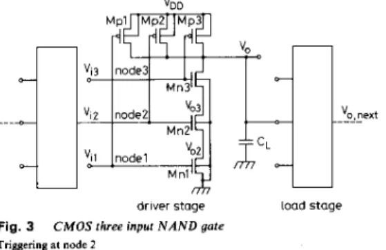
The modified self-scaling and starting quasi-Newton method is implemented as shown in Table 4. In Table 4, the vector g j is the first derivative of the cost function at
x j . The vectors g j , d j , p j , and qj are n x 1 vectors. The vector Sj is a n x n matrix (inverse Hessian). The value a is the optimal step size along the descent direction dj for the minimisation of L,i(x, Aj).
Table 4: Proposed algorithm Step 1
Step 2
Step3 d,=-S,g,,minimiseL,,(x,+cld,,A,),andx,+, = x , + d ,
Step 4
Initial guessx,, evaluatec,, and! = 0 So = 1, calculate g o , A, = 0, and] = 0
If condition A,, go to step 6, else p,=cld,,calculateg,+,.q,=g,+, -g,
A,,, = A , + c , h ( x , ) , and add one to] I f j is smaller than RN. return to step 3 If condition A,. go to step 8 , else x o = x , c,+, =F,,,xc,,andaddonetoi
If I is smaller than iteration, return to step 2 Step 5
Step 6
Step 7
SteD 8 Obtain the solution
The device sizes of each gate are first calculated from the deviated x j by using the timing equation to determine the derivative of the cost function. Dynamic power dissi- pation of the circuit is determined from the calculated device sizes. The derivative of the cost function is approx- imated by the first finite divided difference of the deviated cost function.
There are two iteration loops as shown in Table 4. The inner loop uses the self-scaling scheme to approximate the inverse Hessian matrix S. One complete cycle of an approximation requires at least n steps to approach the result of the conjugate gradient method. Round-off errors, numerical errors, and inaccurate line searches mean that the resultant inverse Hessian matrix may deviate from the actual inverse Hessian matrix and degrade the quadratic convergence rate. A smaller step number R N is assigned to the inner loop. The outer loop is used to construct the restarting scheme of the self- scaling quasi-Newton method. The maximum number of restarting cycles is iteration specified by the user.
There are two check points (A, and A,) in the opti- misation process. A, is used to check whether L , i x j + , ,
,Ij) is 0.99 times larger than L,,(xj, Aj). If that condition is satisfied, the optimisation process restarts. A, is used to check whether L J x j , , 1,) is 0.99 times larger than L&,, Aj). If that condition IS satisfied, the optimisation process
ends and the required timing specifications for each gate is obtained. The device sizes of all the circuit can then be 160
determined by using the timing equations from all the circuit output to all the circuit inputs.
From eqn. 7, it is found that the scale of f ( x ) and IIh(x)ll is not compatible. The penalty parameter co is first normalised to balance the scale of f ( x ) and IIh(x)ll. The subsequent values of c j are monotonically increased using the equation c j + , = F i l Y c j . The value of Fi, is typically larger than 4 and smaller than 10 [21].
The multiplier vector A, is initially chosen to be 0. The subsequent vectors of ,Ij are modified using the equation ,Ij+ = IZj
+
ci x h(xj). Other good modified equations of the multiplier vectors are described in the nonlinear opti- misation text [21-231. The objective of this paper is only to verify the efficiency of the proposed techniques, so the other equations are not considered.5 Experimental results
Using Turbo-C on a PC-AT, the above sizing and opti- misation techniques have been implemented in an experi- mental program called the TISA [19, 201 and applied to size many circuits. The memory required for program and dynamic data is 200 Kbyte and 64 Kbyte/100 gate. The required memory increases quadratically as a func- tion of the gate number because the optimisation method contains a two-dimensional matrix S(x). The maximum number of gates allowed in the optimisation is 128 under the PC-AT 640 Kbyte real-mode limitation. The conju- gate gradient method [23] uses a one-dimensional vector in the optimisation process. Implementing TISA using the conjugate gradient method in PC-AT protection- mode operation (with 16 Mbyte), the maximum number of gates would be expected to be more than 10 OOO.
To demonstrate the efficiency of the proposed tech- niques in the sizing and optimisation, the conventional optimisation algorithms [ 10, 131, were also implemented and applied to size the same circuits. In one of the con- ventional algorithms, the device sizes are used as the vari- ables of the optimisation process and the minimum device sizes are used as the initial guess of the opti- misation process [lo]. It is then called the minimum-size algorithm for simplicity. In the other algorithm, the device sizes are used as variables of the optimisation process and the heuristic approach is used to obtain the initial guess of the optimisation process [13]. It is called the heuristic algorithm for simplicity. The timing models developed [lS-181 are also used in both algorithms for a fair comparison. The increment constant bumpsize [ 131 used in the heuristic approach is 1.1.
Different input excitation nodes lead to different output timing and power consumption. The input excita- tion node of each gate is considered to be the node fur- thest away from the output node to simplify the computation complexity and the computer time in sizing. This can lead to a safe design so that the actual chip delay is always equal to or smaller than that designed. Different input excitation nodes are considered in timing verification.
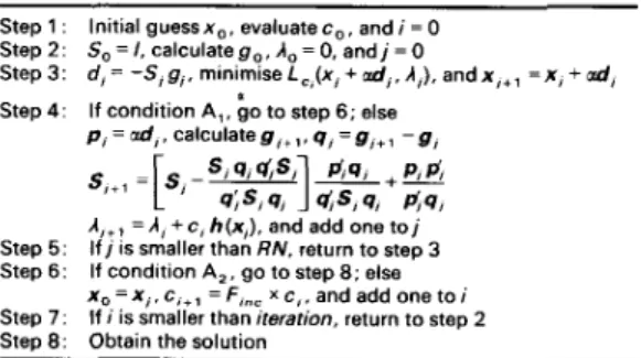
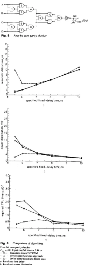
To verify the efficiency of the proposed techniques, the values of Finrr which is the factor associated with the penalty parameters ( c j + , = Fine cj), must be comprehen- sively considered. Both the developed and the conven- tional sizing and optimisation algorithms were applied to size a four-bit even parity checker as shown in Fig. 5. The input voltage was an exponential waveform with a rise/ fall time of 0.44 ns. Using device sizes as optimisation minimisation variables and minimum device sizes as the initial guess, the minimum achievable fixed-delay specifi-
P
Fig. 5 Four bit even parity checker
specified fixed-delay time.ns a
3 5
OI
specified fixed-delay time,ns
b
8 9 10
0: '
i
';
" " 'specified fixed-delay time, ns
C
Fig. 6 Comparison of algorithms
Four bit even parity checker
F,* = 4.0; Input riseffall time = 0.44 ns
-0- transition times/OCWSM - - 0 - - device sires/heuristic approach - - A - - device sizesfminimum device s u e s
a Resultant time delay
b Resultant power dissipation
c CPU time consumption
IEE PROCEEDINGS-E, Vol. 138, N o . 3, M A Y 1991
cation of the optimisation with fixed-delay specification is 7.23 ns. For the optimisations with 5.5, 6, or 7 ns fixed- delay specifications, this algorithm can not respond as can be seen from Fig. 6a. Using device. sizes as opti- misation variables and the heuristic approach to obtain the initial guess, the minimum fixed-delay specification achievable is 611s. The fixed-delay specification of the optimisation using transition times as optimisation vari- ables and the OCWSM to obtain the initial guess can be as small as 5.5 ns. These proposed techniques are called the proposed algorithm.
It is also found that the optimisation with 10 ns fixed- delay specification performed by using the minimum-size algorithm has the local minimum problem. The error between the resultant and the specified delay times is greater than 1%. This phenomenon is not seen in the other two algorithms (the proposed algorithm and the heuristic algorithm).
From Fig. 6b, it is found that the resultant power dis- sipation of the circuit optimised with 8 ns and 9 ns fixed- delay specifications and by using the proposed algorithm are greater than that obtained by using the heuristic algorithm. As the fixed-delay specification decreases to 6 ns and 7 ns, the power dissipation of the circuit opti- mised by using the proposed algorithm becomes smaller than the heuristic algorithm. This means that in high- speed design, the proposed algorithm can perform a more satisfactory optimisation with less resultant power dissi- pation.
In Fig. 6c, it is found that the required CPU time for the optimisations with 7, 8 and 9 ns fixed-delay specifi- cations performed by using the three algorithms are very close. Although the required CPU time for the opti- misation with 6 ns fixed-delay specification performed by using the proposed algorithm is 30% greater than that by using the heuristic algorithm, the power dissipation of the circuit optimised by using the proposed algorithm is smaller. The trade-off between CPU time and circuit per- formance is thus satisfactory in the proposed algorithm.
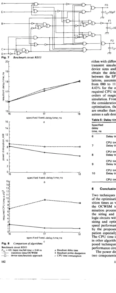
To further verify the efficiency of the optimisation process by using the proposed algorithms for the complex circuit, a benchmark circuit RD53 [37] shown in Fig. 7 was optimised. It contains CMOS standard static logic gates and A 0 1 gates. The given input rise/fall time is 0.44 ns. The fixed-delay specifications at nodes FO, F1, and F2 are considered to be the same. Fig. 8 shows the comparisons between the optimisation results of the proposed algorithm and the heuristic algorithm. The optimisation using the minimum-size algorithm can not satisfy the specified delay time and so it is not shown in Fig. 8. It is found from Fig. 8a that the heuristic algo- rithm and the proposed algorithm can satisfy the delay specification. As seen from Fig. 8b, the power dissipations obtained by using the proposed algorithm are smaller than those obtained by using the heuristic algorithm. This is because the h(x) in the cost function is nearly pro- portional to the optimisation variable. The relation between the cost function and the optimisation variables of the proposed algorithm is more linear than that of the heuristic algorithm. The proposed algorithm can thus avoid the incorrect optimisation convergence caused by the numerical errors and inaccurate line searches from the first finite divided difference of the deviated cost func- tion. These characteristics also make the CPU time of the proposed algorithm smaller than that of the heuristic algorithm (Fig. Sc).
To verify the accuracy of the adopted timing models, a one-bit full adder is sized by using the proposed algo-
IF
Fig. 7 Benchmark circuit RD53
15
16 17 18
specified fixed-delay time, ns
a
3 E
“1
120
z
:
d
16 17 18specified f ixed-deloy time. n s
:g
13
b
specified fixed-delay time,ns Fig. 8 Comparison of algorithms
Benchmark circuit RD53
F,, = 4.0; Input rise/fall time = 0.44 ns
-0- transition times/OCWSM b Resultant power dissipation
-- 0 - - device sizes/heuristic approach c CPU time consumption 162
4 Resultant delay time
rithm with different fixed-delay specifications. The SPICE transient simulations of the circuit with the obtained device sizes and the given input excitation is made to obtain the delay time. Table 5 lists the comparisons between the SPICE simulations and the model calcu- lations, assuming that the input modes ABC changes from 0o0 to 111. The maximum error is 13.29% and 4.43% for the outputs sum and carry, respectively. The required CPU time of the model calculation is about two orders of magnitude smaller than that of the SPICE simulation. From Table 5, it is also found that because of the consideration of worst-case timing in the sizing and optimisation, the resultant delay times of sum and carry are smaller than the fixed-delay specifications. This guar- antees a safe design.
Table 5 : Delav times of one-bit full adder
~
Specified delay time, ns
SPICE Model Error
Yo
6 Delay time, ns Sum
Carry CPU time (PCjAT), s
7 Delay time, ns sum
carry CPU time (PCjAT). s
8 Delay time, ns sum
carry CPU time (PCjAT). s
9 Delay time, ns sum
carry CPU time (PCjAT), s 10 Delay time, ns sum carry CPU time (PC/AT), s
3.161 5.01 5 500 4.186 5.598 399 4.722 6.228 372 6.1 91 7.206 6.062 7.874 387 384
-
2.733 13.29 4.782 4.43 3.720 10.94 5.362 4.06 4.306 8.63 5.986 3.75 6.112 1.13 7.142 0.76 5.937 1.91 7.667 2.50 2 2 2 2 26 Conclusion and discussion
Two techniques were proposed to enhance the efficiency of the optimisation process. The techniques use the tran- sition times as variables of the optimisation process and the OCWSM to obtain the initial guess of the opti- misation process. The proposed techniques can perform the sizing and optimisation of CMOS combinational logic circuits with a smaller delay specification than other sizing and optimisation algorithms. This enhances the speed performance of the sized circuits. The circuit sized by the proposed algorithm has a smaller power dissi- pation especially when the delay specification is small. The CPU time is of the same order of magnitude as that in other algorithms. It is therefore suitable to use the pro- posed techniques in the sizing and optimisation of high- performance circuits.
The power dissipation of CMOS logic gates consists of two components: dynamic power dissipation and short- IEE PROCEEDINGS-E, Vol. 138, N o . 3, M A Y 1991
circuit power dissipation. The power dissipation con- sidered earlier is the dynamic power dissipation. To accurately calculate the power dissipation of a CMOS logic circuit, an accurate model of the short-circuit power dissipation for CMOS logic gates must be constructed. This is the intention of a future study.
There are many design considerations for a CMOS logic gate such as equal rise and fall times, equal channel widths of PMOSFET and NMOSFET, equal high and low noise margin, optimal ratio of each gate, etc. The design consideration with symmetrical rise and fall times is adopted as used in the above optimisation. All the design considerations can be arranged to use the tran- sition time as the optimisation variables so it is expected that by using the proposed techniques, the above men- tioned advantages can be also obtained.
The proposed techniques can be applied to other sizing and constrained optimisation problems. Further generalisation of the proposed algorithm in solving various problems will be performed in the future.
7 References
1 NYE, W., POLAK, E., SANGIOVANNI-VINCENTELLI, A., and TITS, A.: ‘DELIGHT: An optimization-based computer-aided design system’. Proc. Int. Symp. Circuits and Systems., 1981, pp. 851-855
2 BRAYTON. R., HACHTEL, G., and SANGIOVANNI- VINCENTELLI, A.: ‘A survey of optimization techniques for integrated-circuit design’, Proc. I E E E , 1981,69, pp. 1334-1362 3 KANUMA, A.: ‘CMOS circuit optimization’, Solid-State Electron.,
1983,26, pp. 47-58
4 TRIMBERGER, S.: ‘Automated performance optimization of custom integrated circuits’. Proc. Int. Symp. Circuit and Systems,
1983, pp. 196197
5 LEWIS, E.: ‘Optimization of device area and overall delay for CMOS VLSI designs’, Proc. I E E E , 1984,72, pp. 6 7 M 8 9 6 GLASSER, L.A., and HOYTE, L.P.J.: ‘Delay and Power opti-
mization in VLSI circuits’. Proc. 21st Design Automation Conf., 1984, pp. 781-785
7 VEENDRICK, H.J.M.: ‘Short-circuit dissipation of static CMOS circuitry and its impact on the design of buffer circuits’, I E E E
Trans., 1984, SC-19, pp. 4 6 8 4 7 3
8 LEE, C.M., and SOUKUP, H.: ‘An algorithm for CMOS timing and area optimization’, I E E E Trans., 1984, SC-19, pp. 781-787 9 KAO, W.H., FATHI, N., and LEE, C.H.: ‘Algorithms for automatic
transistor sizing in CMOS digital circuits’. Proc. 22nd Design Automation Conf., 1985, pp. 781-785
IO MATSON, M.D., and GLASSER, L.A.: ‘Macromodeling and opti- mization of digit MOS YLSI circuits’, I E E E Trans., 1986, CAD-5,
pp. 659-678
11 HEDENSTIERNA, N., and JEPPSON, K.O.: ‘CMOS circuit speed and buffer optimization’, I E E E Trans., 1967, C A D d , pp. 270-281 12 CIRIT, M A : ‘Transistor sizing in CMOS circuits’. Proc. 24th
Design Automation Conf., June 1987, pp. 121-124
13 SHYU, J.M., SANGIOVANNI-VINCENTELLI, A.J., FISHBURN, P., and DUNLOP, A.E.: ‘Optimization-based transistor sizing’, I E E E Trans., 1988, SC-23, pp. W O 9
14 RICHMAN, B.A., HANSEN, I.E., and CAMERON, K.: ‘A deter- ministic algorithm for automatic CMOS transistor sizing’, I E E E
Trans., 1988, SC-23, pp. 522-526
15 WU, C.Y., HWANG, J.S., CHANG, C., and CHANG, C.C.: ‘An efficient timing model for CMOS combinational logic gates’, I E E E
Trans., 1985, CAD-4, pp. 6 3 6 6 5 0
16 WU, C.Y., LI, C., and HWANG, J.S.: ‘Timing macromodels for CMOS static setireset latches and their aoolications’.
..
I E E E Proc. E.1988,135, pp. 151-160
17 WU, C.Y., and HWANG, J.S.: ‘Physical timing models of small- geometry CMOS inverters and multi-inout NAND/NOR eates and their applications’, Solid-State Electron., ‘1989,32, (6), pp. 44k467. 18 WU, C.Y., and SHIAO, M.C.: ‘General and efficient timing models
for CMOS AND-OR-INVERTERS and OR-AND-INVERTERS gates’, I E E E Trans., 1991, CAD-IO
19 WU, C.Y., and HWANG, J.S.: ‘A new autosizing algorithm for CMOS combinational logic circuits’. Int. Symp. VLSI Technology, Systems and Applications, 1989, pp. 242-246
20 WU, C.Y., and HWANG, J.S.: ‘A new fast sizing algorithm for bigh- I E E PROCEEDINGS-E, Vol. 138, No. 3, M A Y 1991
performance CMOS combinational logic circuits’. 3rd Int. Symp. IC Design and Manufacture, 1989, pp. 165-172
21 BERTSEKAS, D.: ‘Constrained optimization and lagrange multi- plier methods’ (Academic Press, 1982)
22 GILL, P.E., MURRAY, W., and WRIGHT, M.H.: ‘Practical opti- mization’ (London, 1981)
23 LUENBERGER, D.: ‘Introduction to linear and nonlinear prog- ramming’ (Addison-Wesley, 1984)
24 SHJOI, M.: ‘CMOS digital circuit technology’ (Prentice-Hall, Englewood Cliffs, 1988)
25 KANG, S.M.: ‘A design of CMOS polycells for LSI circuits’, I E E E
Trans., 1981, CAS-28, pp. 838-843
26 TOKUDA, T., OKAZAKI, K., SAKASHITA, K., OHKURA, I., and ENOMOTO, T.: ‘Delay-time modeling for ED MOS logic LSI’, IEEE Trans., 1983, CAD-2, pp. 129-134
27 ETIEMBLE, D., ADELINE, V., DUYET, N.H., and BALLEGEER, J.C.: ‘Micro-computer oriented algorithms for delay evaluation of MOS gates’. Proc. 21st Design Automation Conf., 1984, pp. 358-364 28 BAYRUNS, R.J., JOHNSTON, R.L., FRASER JR., D.L., and FANG, S.-C.: ‘Delay analysis of Si NMOS Gbit/s logic circuit’, IEEE Trans., 1984, SC-19, pp. 7 5 5 7 6 4
29 SIMONNS, I.G., and TAYLOR, G.W.: ‘An analytical treatment of the performance of submicrometer FET logic’, I E E E Trans., 1985, SC-20, pp. 1242-1251
30 AUVERGNE, D., CAMBON, G., DESCHACHT, D., ROBERT, M., SAGNES, G., and TEMPIER, V.: ‘Delay-time evaluation in ED MOS logic LSI’, I E E E Trans., 1986, SC-21, pp. 337-343
31 DESCHACHT, D., ROBERT, M., and AUVERGNE, D.: ‘Explicit formulation of delavs in CMOS data Datbs’, I E E E Trans., 1988, SC-23, pp. 1257-1264
32 BROCCO, L.M., MCCORMICK, S.P., and ALLEN, J.: ‘Macro- modeling CMOS Circuits for timing simulation’, I E E E Trans., 1988, CAD-7, pp. 1237-1249
33 JOUPPI, N.: ‘Timing analysis for nMOS VLSI’. Proc. 20th Design Automation Conf., 1983, pp. 4 1 1 4 1 8
34 PLONUS, M A : ‘Applied electromagnetics’ (McGraw-Hill, New York, 1978)
35 DESOER, C.A., and KUH, E.S.: ‘Basic circuit theory’ (McGraw- Hill, New York, 1978)
36 VLADIMIRESCU, A., and LIU, S.: ‘The simulation of MOS Inte- grated Circuit Using SPICEI. Memorandum M80/7, 1980 37 MITCHELI, M.D., SANGIOVANNI-VINCENTELLI, A., and
ANTOGNETTI, P.: ‘Design system for VLSI circuits logic synthesis and silicon compilation’ (Netherlands, 1981)
8 Appendix
The change of the energy stored on the drain-bulk junc- tion capacitor is derived. The energy loss of a passive element from time to to t f is [35]
(9) Since i(t’) at’ = 84, the above equation can be rewritten as
4Qo,
QA
=
E V ( Q 7a Q
(10) The drain-bulk junction capacitance [36] is a voltage- dependent capacitor and can be expressed asA D P D
M J S W
( I
+g)
C j = CJ
where CJ is the zero-bias bulk capacitance per square metre, M J is the bulk-junction grading coefficient, A, is the drain area, P , is the drain perimeter, VD, is the voltage across the drain-bulk junction, CJSW is the zero- bias perimeter capacitance per metre, MJSW is the perimeter grading coefficient, C,,, is the bulk capac- itance and Cleri is the perimeter capacitance.
The energy loss of a passive element from time t , to time tl (from V D , = Vo = 0 to V D , = V, = V,,J can be
- 7 - T -
rewritten as
Qr
4Q01
Q,)
=
JQo V ( Q )a Q
Thus, the energy loss of the drain-bulk junction capac- itance is expressed as &drain = C J A ~ ~ , , ~ A v b i d
+
C J S w P D F p e r d v b i o s ) (15) where = [ V ( Q ) Q ]IQ’
- Jv’Q(V‘) d V ‘ Qo Y o =[(c,
v)vl
I“=”
-Jv’(cj
v)
a r
(12) v=vo YoThe energy loss caused by the area capacitance &‘a,ee is
Similarly, the energy loss caused by the perimeter capac- itance B,,, is v ; i G s dperi = C J S W P ,