ELSEVIER Thin Solid Films 346 r1999) 186-190
Effects of BF: implantation on the oxidation resistance of copper films
Zhen-Cheng Wu*, Yu-Lin Liu, Mao-Chieh Chen
Deparhnenr of Elecrronics Engineering and the Institute of Electronics, National Clko-Tung Ukersity, 1001 Ta Hsueh Road, Hsinchu 300, Taiwan
Received 16 April 1998; received in revised form 27 October 1998: accepted 10 November 1998
Abstract
This work investigates the effects of BF; implantation on the oxidation resistance of copper films. The BFT ions were implanted into Cu films through a 1000 w thick screen SiOl layer. We found that the oxidation resistance of Cu films can be significantly improved by BFT implantation at appropriate conditions. In particular. SF; implantation at 35 to 30 keV to a dose of I -8 x 10” cm-’ made the Cu films capable of resisting oxidation at temperatures up to 250°C. At these BF’implantation energies, boron atoms of peak concentration were projected near the Cu surface; thus the diffusion paths of oxidizing species were efficiently blocked. Implantation at too high energy would result in greater depth of projection, thus a lower concentration of boron at the Cu surface; moreover. it generally leads to increased
implantation defects that might serve as diffusion paths for the oxidation species. On the other hand, too high dosage implantation would also have an adverse effect on the capability of oxidation resistance for Cu films owing to the higher density of implantation damage as well
as the formation of reactive fluorine compound (CuF?) near the Cu surface. 0 1999 Elsevier Science S.A. All rights reserved. Keyir’ords: Copper; Oxidation; Boron; Fluorine
1. Introduction
Copper has been extensively studied as an alternative to the Al-based alloys for the next generation ultra large scale integration (ULSI) applications because of its low resistivity (1.72 ~sl cm) and superior electro/stress-migration charac- teristics [ 11. However, copper oxidizes easily on its exposed surfaces at low temperatures in the ambient normally used in the ULSI back-end process and this characteristic becomes a serious concern for integration with high temperature (>4OO”C) metallization process. To improve the oxidation resistance of copper films. a number of meth- ods have been investigated, one of which is to implant a small amount of impurities in copper so as to modify its surface properties while retain its inherent bulk benefits. The impurity species that have been studied include B, N, Ti. Mg, Al, and Cr [2-71. Naguib et al. implanted B ions into polycrystalline Cu and concluded that the implantation of B ions reduced the oxidation of Cu at 200°C irrespective of the ion energy [7]. Moreover, Ding et al. reported that corrosion resistant Cu films were obtained by B ion implantation at 50 keV to a dose of (I-5) x IO’” cme2 [8,9]. Similar results were found for corrosion resistance of materials other than copper. Rubio et al. reported that the corrosion resistance of steam generator material (Inconel 600) could be enhanced
* Corresponding author. Tel.: + 3-571-2121; fax: + 3-572-4361.
E-mail address: [email protected] (Z.C. ?Vu)
by implanting the near-surface region with high energy BFT ions [IO].
In this work, we investigated the effect of BFT ion
implantation on the oxidation resistance of copper films. Effort was made to determine the optimal implantation condition with respect to its effectiveness in improving- the oxidation-resistant capability of copper films.
2. Experimental details
The experimental samples used in this study were prepared on p-type (100) oriented Si wafers of 3 inch diameter. After initial RCA cleaning, a 2000 A thick Si& was thermally grown at 1050°C in dry oxygen atmosphere. Copper films of 2000 A thi%ness were sputter deposited on the SiOl covered substrate. The base pressure for the Cu
deposition was 1.5 X 10U6 Torr, and the Cu films were sfiut-
ter deposited using a pure Cu target in Ar ambient at a pressu!e of 7.6 X 10m3 Torr. A capping oxide layer of 1000 A thickness was then deposited; the oxide was RF sputter deposited using an ,302 target in Ar ambient at a pressure of 7.6 x lo-” Torr. This capping oxide was delib-
erately used to prevent the ion beam in the subsequent BFC implantation from directly impinging upon the underlayer copper film so as to retain its integrity and avoid unwanted contamination, such as hydrocarbon, which might adhere to the surface from the environment bkfore the ox$Gion proceeded. The samples were implanted with BFf ions at
0030~6090/99/$ - see front matter 0 1999 Elsevier Science S.A. AU rights reserved.
Z,C. Wu et al. /Thin Solid Film 346 (1999) 186-190 187
(4
Cu(;lll)As-deposited
20 25 30 35 40 45 50 55 60 65 70
28 (degree)
Fig. 1. XRD spectra for as-deposited and thermally treated Cu films (2000A thickness) on Si02/Si substrates: (a) unimplanted samples, (b) samples implanted with BF: at 35 keV to a dose of 5 X 10’” cm-‘, and tc) samples implanted with BFf at 50 keV to a dose of 5 X IO’” cm-2.
an energy ranging from 25 to 50 keV to a dose of 5 X 10’” to
5 X IO’” cm-‘. After the ion implantation, the capping oxide
was removed by reactive ion etching (RIE). The wafers were cut into pieces with a sample size of 1.5 X 1.5 cm2
each for oxidation study. The samples were baked on a hot plate in open air at a temperature ranging from 150 to 300°C for 30 min.
275 r
125 (I . I,
0 25 30 35 40 45 50
Implantation Energy (keV)
Fig. 2. Degradation temperature (Td) of Cu films versus BF: implantation energy; the implanted dose is 5 X 10’” cm-*.
0.0 0.1 0.2 0.3 0.4 0.5 0.6
Depth (microns)
0.0 0.1 0.2 0.3 0.4 0.5 0.6
Depth (microns)
Fig. 3. SIMS depth profiles for Cu/SiOJSi samples implanted with BFT ions to a dose of 5 x IO” cm-’ at an energy of 35 keV (a) before and (b) after thermal treatment in air at 250°C.
The oxidation behavior of the ion implanted Cu films was characterized by various techniques and measurements. The sheet resistance (RR,) of the samples was measured by a four point probe. The crystallinity of films was studied using X- ray diffraction (XRD) analysis. Surface morphology was observed using scanning electron microscope (SEM). Secondary ion mass spectroscopy (SIMS) was used to measure the elemental depth profiles, and X-ray photoelec- tron spectroscopy (XT’S) was employed to study the elemen- tal chemical states.
3. Results and discussion
Fig. 1 shows the typical examples of XRJI spectra for the as-deposited and thermally treated Cu films of 2000 A thick- ness with and without BF; ion implantation. The distinct Cu(ll1) diffraction peak indicates that the film is highly [ 11 II-oriented, a characteristic of the copper films. The diffraction peak of cuprous oxide Cu?O started to appear after the samples were thermally treated at a certain tempera- ture: which is designated as the degradation temperature (r,)
188 Z.C. Wrc et ai. I Thin Solid Film 346 (1999) 186-190 10000 s '5 8000
??
2
6000 2 2 4000 E ; 2000 I(a)
cu2p Sputtering . (1) 1 min (2) IO min , (3) 20 min I - 932.5 eQ I a-5 eQ I 3200 s .= 2800 5 $ 2400 L se P $ 2000 z 2 1600 al I 1200 i26 928 930 932 934 936 938Binding Energy (eQ)
520 525 530 535 640 545 550
Binding Energy (eV)
Fig. 4. XPS spectra showing the chemical states of (a) Cu:p and (b) 0,s photoelectrons for Cu/Si02/Si samples implanted with BF,f ions at 35 keTr to a dose of 5
x
10” cm-’ and thermally treated in air at 750°C.hereafter. The degradation temperatures (Td) were found to be 175°C for the unimplanted as-deposited Cu films, 250°C for Cu films implanted with BF; at 35 keV to a dose of 5 X
10” cm-l, and 175°C for Cu films implanted with BFT at 50 keV to the same dose. It is worth noting that the sheet resistance of Cu/SiOZ/Si samples made a drastic increase when the samples were thermally treated at their respective degradation temperatures (Td). Fig. 2 shows the degradation temperatures {Td) for Cu films implanted with BF; ions to a dose of 5 X 10” cm-’ at various energies. We found that the implantation at energies of 35 and 40 keV was the most effective in retarding the oxidation of Cu film. Fig. 3 shows the SIMS depth profiles for Cu/SiO#i samples implanted with BFT ions to a dose of 5 X 10IJ cm-’ at an energy of 35 keV. The implantedboron atoms were located basically at the Cu surface in a very shallow region (Fig. 3a); this boron- rich layer is expected to retard the penetration of oxygen, and thus improve the oxidation resistance of Cu films [7-9,111. Implantation at higher energies would result in greater depth of maximum boron concentration, and less oxidation resis- tance would be anticipated because of a lower concentration
of implanted boron atoms neaf the surface. This presumption was confirmed in view of the dose dependence to be reported later. Moreover, higher implantation energies generally lead to increased implantation defects [6]. These defects might
serve as diffusion paths for the diffusion of oxidizing species. For the BFT implanted Cu/SiO$Si samples thermally treated in air at 250°C. the boron distribution profile had a dramatic change (Fig. 3b); the as-implanted maximum boron concen- tration near the Cu surface disappeared, and the boron atoms were distributed throughout the Cu film resulting in rapid oxidation at this temperature. Similar phenomena were observed for the samples implanted at -other energies. Fig. 4 shows the XPS spectra of CuZp and OIs photoelectrons for the BF; implanted and 250°C thermally treated Cu/SiO&i sample. The spectra clearly show that a cuprous oxide (CulGj layer was formed on the Cu film, and the intensity of the Cu:O peak decreased gradually with Ar-sputtering time. From the experimental data, it was observed that the peak of pure copper at 932.7 eV evolved after further Ar sputtering, and no reactive fluorine compounds were detected. Fig. 5 shows the surface morphology for the as-deposited and thermally treated Cu films with and without BFT ion implantation. The as-deposited Cu films had smooth surfaces and dense strut- tures which is a characteristic of sputtered Cu films (Fig. 5a), while impiantation induced surface defects are clearly observed on the BFT implanted samples (Fig. 5b). DiEuGon via these surface defects might play an important role in the oxidation behavior ofCu films. After thermal treatment of the as-deposited Cu films and the BFT implanted Cu films at their respective degradation temperature, which is 175°C for the former and 250°C for the latter, cuprous oxide (0~~0) was present on the surfaces of unimplanted samples (Fig. 5c) as well as BFT implanted samples (Fig. 5d), as confirmed by the XPS analysis (Fig. 4). The Cu-0 oxide was discontinuous as well as porous in nature [12], thus allowing diffusion to proceed through the pores. Moreover, thermal treatment at higher temperatures resulted in easier grain growth and thus larger grain size, as can be seen by comparing Fig. 5c with Fig. Sd.
Fig. 6 shows the degradation temperatures (TJ for Cu films implanted with BFT ions at 35 keV to various doses. We found that the optimum dose was in the order of 10’” cm-’ for the purpose of oxidation resistance. For the samples with implanted dose of 5 x 10’” cm-‘, Td was lowered to 175°C. The results of TEM analysis Cn_ot shown) indicated that the high dose c.5 x 10’” cm-Flat
35 keV) implanted samples remained in a polycrystalline structure, similar to the medium dose (of the order of IO” cm-‘) implanted samples. However. high dosage implanta- tion is expected to result in higher damage density near the surface of implanted samples [13,14]. These high density defects could enhance diffusion of oxygen into Cu films, thus promoting the formation of copper oxide, Hence. implantation dose greater than 5 X IO” cm-’ would dete-
riorate the capability of oxidation resistance relating to the damage density instead of the post-implant microstructure.
189
0
a
Fig. 5. SEh4 micrographs showing surface morphology for Cu films (a) as-deposited, (b) implanted with BF; at 35 keV to a dose of 5 X 10” cm-‘; (c) sample of (a) after thermal treatment at 175”C, and (d) sample of (b) after thermal treatment at 250°C.
Moreover, high dose BF; implantation (5 X lOI cm-‘)
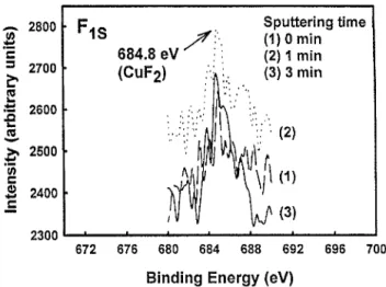
resulted in high concentration of fluorine as well as boron near the Cu surface, as shown in SIMS depth profiles illu- strated in Fig. 7. It has been reported that high concentration of boron near the surface region would block the diffusion path for oxidizing species including CuT ions [7-9,113; however, enhanced oxidation might also occur as a result of the formation of reactive fluorine compounds [lo]. The XPS spectra shown in Fig. 8 indicates the formation of cupric fluoride (CuF:) phase [15] near the Cu surfaces for Cu films implanted with BFf ions to a dose of 5 X 10’”
cm -‘; the fluorine compound was not detected in Cu films implanted with BFC ions to a dose less than 1 X lOI cm-?.
The formation of CuF? compound was presumably asso-
ciated with agglomeration of implanted fluorine ions above a certain dose [16]. This might have an adverse impact on degrading the capability of oxidation resistance for Cu films. The competing effect between boron and fluor- ine in the high dosage BFT implanted samples (5 x lOI
cm-“) resulted in lowered degradation temperature. For the sample structure employed in this work, the BFT implantation at an energy of 35 keV must be limited to a dose no more than 1 X 10’” cme2.
4. Conclusions
190 Z.C. Wit et al. /Thin Solid Films 346 (1999) 186-190
150 I,,.
0 1 5 IO 50 100 500
Dose (~10’~ cma2)
Fig. 6. Degradation temperature (T,) of Cu films versus implanted dose of BFT ions; the implantation energy is 35 keV.
tures below 175°C in air. With appropriate BF; implanta- tion into Cu films, the oxidation resistance of Cu films can be improved. The optimum condition of l3F; implantation is to place boron atoms of proper concentration near the Cu surface so as to block the diffusion path for oxidizing species? i.e. oxygen and Cu atoms. Implantation at too high energy would result in greater depth of projection, thus a lower concentration of boron at the Cu surface. and generally lead to increased implantation defects that might serve as diffusion paths for the oxidizing species. On the other hand, too high dosage implantation would also have an
adverse effect on the capability of oxidation resistance for Cu films due to the higher density of implantation damage as well as the formation of reactive fluorine compound (CuFl) near the Cu surface. We found that the best results can be obtained by BFT implantation at 35 to 40 keV to a dose of (l-8) X 10” cm-‘. With BF; implantation at these
conditions, Cu films were able to resist oxidation at temperatures up to 250°C.
0.0 0.1 0.2 0.3 0.4 0.5 0.6 Depth (microns)
Fig. 7. SIMS depth profiles for Cu/SiO,/Si samples implanted with BF- ions to a dose of 5 X IO’” cm-’ at an energy of 35 keV followed by thermal treatment at 175°C.
’
FIS time2300 ’ ’
672 676 680 684 688 692 696 700
Binding Energy (eV)
Fig. 8. XPS spectra showing the chemical state of Fls photoelectrons for Cu/SiO#i samples implanted with BFT ions at 35 keV to a dose of 5 x
10’” cm-’ followed by thermal treatment in air at 175°C
Acknowledgements
The authors wish to thank Messrs Y.C. Lee, Y.L. Chin, and M.T. Wang. as well as MS P.J. Lin for their technZ1 assistance. Thanks are also due to Mr J.C. Chuang for stimu- lating discussion. This work was supported by the National Science Council (ROC) under Contract No. NSC 87-22I5- E009-072.
References
[l] T. Takewaki, R. Kaihara, T. Ohmi, T. Nitta. IEDM Tech Dig. (1995j 253.
[?I D.C. Kothari, L. Gunman. S. Girardi. A. Tom&. S. Gialanella, plh;l. Raole, P.D. Prabhawalkar, Mater. Sci. Eng. Al 16 (1989) 135. ~ [3] L.G. Svendsen. S.S. Eskildsen, P. Borgesen. Thin Solid Films 110
(1983) 237.
[4] L.G. Svendsen, Corrosion Sci. 10 (1980) 63.
[5] P.J. Ratcliffe, R.A. CoIlins. Phys. Status Solidi A 78 (1983) 547, [6] P.J. Ratcliffe, R.A. Collins, Phys. Status SoIidi A 108 (1988) .537- [7] H.M. Naguib, R.J. Kriegler. J.A. Davies, J.B. Mitchell, J. Vat. Sci.
Technol. 13 11976) 396.
[8] P.J. Ding, W.A. Lanford. S. Hymes, S.P. Murarka, Mater. Res. Sot. Symp. Proc. 260 (1992) 757.
[9] P.J. Ding, W.A. Lanfurd, S. Hymes, S.P. hturarka, J. Appl. Phys.73 (1993) 1331.
[lo] J.D. Rubio. R.R. Hart, R.B. Griffin, Corrosion 32 (1986) 557* ~~ [ll] P.J. Ding, W. Wang, W.A. Lanford, S. Hymes, S.P. Mum&a, NZZi.
Instrum. Methods Phys. Res. B 55 (199-l) 260.
[12] J. Oudar, Physics and Chemistry of Surfaces, Blackie, Glasgow, 1475, pp. U-93.
[13] S. Wolf, Silicon Processing for the VLSI Era ii). Lattice Press, Sunset Beach, 1990, p. 299.
[14] S.P. Speakman, R.A. CoIlins, G. Dearnaley. Appl. Phys. A 35 (1984) 99.
[l5] S. Bahadur. D. Gong, J.W. Anderegg, Wear 165 (1993) 205. ~~ [16] T.B. Massalski, H. Okamoto, P.R. Subramanian. L. Kacprzak. BiZ?y