Effects of (002)
β-Ta barrier on copper chemical mechanical polishing behavior
Yu-Sheng Wang
a, Kei-Wei Chen
b,⁎
, Min-Yuan Cheng
c, Wen-Hsi Lee
a, Ying-Lang Wang
da
Department of Electrical Engineering, National Cheng Kung University, Tainan 701, Taiwan, ROC
b
Department of Materials Science, National University of Tainan, Tainan 700, Taiwan, ROC
cDepartment of Materials Science and Engineering, National Chiao Tung University, Hsinchu 300, Taiwan, ROC d
College of Photonics, National Chiao Tung University, Tainan 711, Taiwan, ROC
a b s t r a c t
a r t i c l e i n f o
Available online 9 June 2012 Keywords:
Semiconductors Barriers
Chemical mechanical polishing
This study proposes that the corrosion resistance of copperfilm correlates well with underlying barrier's ori-entation. To test the hypothesis, we performed X-ray diffraction, conducted copper removal rate experiments after chemical mechanical polishing, and tested static potentiodynamic polarization. The results all show that copper deposited on strongly (002) orientedβ-Ta barrier layer demonstrated better chemical resistance against surface reaction with the slurry for strong copper (111) orientation. Thefindings were consistent with the result of the chronoamperometric test at 0.3 V in which the more passivefilm formed on the com-positefilm with (002) β-Ta underlying barrier.
© 2012 Elsevier B.V. All rights reserved.
1. Introduction
Copper has replaced aluminum as the interconnect metal in inte-grated circuits due to its higher electrical conductivity and superior electromigration resistance. It has recently been reported that the resistance to copper electromigration is closely related to the texture of copperfilms with the (111) orientation[1,2]. An effectively under-lying barrier layer is necessary to prevent the diffusion of copper ions through the dielectric layer. Researchers have pointed out that vari-ous underlying barrier materials and textures will affect the micro-structure of electroplated copper films [3–8]. Wong et al. [4] demonstrated that the grain boundaries of Ta are often directly aligned with the grain boundaries of copper. Kwon et al.[9] men-tioned that using (002)β-Ta as an underlying barrier layer enhances the (111) texture of the copperfilm with a heteroepitaxial growth.
In most production processes, electrochemical plating is the pri-mary method of copper metallization. After electroplated copper de-position, chemical mechanical polishing (CMP) is a necessary step for surface planarization in microelectronic industry. In a typical CMP process, material is removed from the surface of a wafer through the combined chemical and mechanical actions of slurry containing abrasive particles and weak etchants. The famous polishing principle for the removal rate simulation is Preston's equation, as described below[10,11]:
RR¼ kPn
Umþ RR0
where RR is the material removal rate and k is the Preston's constant. P is the applied wafer pressure and U is the average linear pad-wafer
velocity. RR0represents the dynamic etch rate of the material in the absence of pressure and velocity. This equation is very general since it relies on essentially one constant, k, to account for all chemical and mechanical intricacies of the process. Although many studies es-tablish various removal models to describe polishing behavior, a sim-ple relationship between the removal rate and CMP parameters can be obtained if we consider only the basic mechanics, which is that the removal rate is direct proportion to the applied polish pressure.
The removal rate of copper during CMP is closely correlated with the corrosion resistance of the electrochemical deposition films. Higher corrosion current density means higher copper removal rate during polishing. To test corrosion, Lin et al. [12,13] used the potentiodynamic polarization for electrochemical measurement and found that copper polished surface with high (111)/(200) ratio has strong chemical resistance. In the potentiodynamic polarization curve[14], using extrapolation method can get corrosion current den-sity (Icorr)[15].
While the effect of underlying barrier layer on the performance of the electrochemical platingfilm has been widely studied, the sequen-tial effect on the CMP behavior has not been fully identified. The ob-jective of this paper is thus to describe the relationship between the textures of tantalum barrier and the behavior of chemical mechanical polishing, withfindings from X-ray diffraction analysis, copper CMP removal rate, and potentiodynamic polarization measurements. This paper will conclude that the corrosion resistance of copperfilm was highly correlated with underlying barrier's orientation.
2. Experimental details
Cu electrochemical deposition on blanket 12-inch Si (100) wafers had the substrate condition with 500 nm thermal oxide. Two series of
Thin Solid Films 529 (2013) 435–438
⁎ Corresponding author.
E-mail address:kwchena@hotmail.com(K.-W. Chen).
0040-6090/$– see front matter © 2012 Elsevier B.V. All rights reserved. doi:10.1016/j.tsf.2012.06.017
Contents lists available atSciVerse ScienceDirect
Thin Solid Films
tantalum barrierfilms were prepared with 15 nm-thick by physical vapor deposition at room temperature based on the previous study of Wang et al.[16], which described the textures of Ta/TaN barriers sputtered with various N2/Ar ratios: (1) deposited with 10% N2/Ar ratio, which was called Barrier A. N2 and Ar were applied into sputtering at the same time to form TaN structure; (2) deposited with putting Ar into chamberfirst, then using N2 to make Ta becomes TaN, which was called Barrier B. 100 nm thick copper seed layers used as the conductive layer of sequential electrochemical deposition were deposited on Barrier A and Barrier B with 56 kW DC power and 500 W AC bias, which were called Film AS and Film BS, respectively. Ele-ctroplating was carried out using 15 °C bath control with a 12 L/min steady overflow rate. Electroplating studies were performed in a con-ventional acid copper sulfate electrolytic solution containing 50 g/L copper metal, 20 g/L sulfuric acid, and 80 mg/L chloride ions with a small amount of proprietary organic additives. The thickness of the electroplating copper samples was 200 nm; they were called Film ASP and Film BSP, which were plated on the corresponding copper seed layers. For CMP, the polishing conditions were at head rotation speed of 63 rpm, platen rotation speed of 70 rpm and normalized polishing pressure of 1 to 40 kPa. The copper polishing slurry was prepared with 3.1 wt.% fumed aluminum particle and an acid solution with pH 3–5, which contained ingredients, including 0.2 wt.% hydro-gen peroxide, 1 wt.% passivation ahydro-gent (BTA) and a glycine acid salt which is commonly used in copper CMP slurries as a buffering and chelating agent. The peroxide and passivation agent were used as ox-idizer and inhibitor for this study, respectively.
X-ray diffraction method was applied to determinefilm textures of tantalum barrier layers, copper seed layers, and electroplated copper layers, respectively. The X-ray diffraction apparatus model was Bruker AXS D8 Advance platform with in-situ cell Anton Paar HTK 1200 N, Cu Kalpha for X-ray source, and Bragg–Bentano configuration. The removal rates of copperfilms after chemical mechanical planarization were measured by the four-point probe method using a 49 point line scan on a Prometrix resistance measurement tools. Potentiodynamic polari-zation curve and chronoamperometric (applying potential) measure-ment for corrosion current study were performed with a computer-controlled CHI-602A potentiostat. Three-electrode cell was used for electrochemical measurement. The working electrode (test specimen) was prepared from 12-inch wafer that was processed with barrier, cop-per seed, and electroplated copcop-per layers (Film ASP and Film BSP). The specimen size was 1 × 10 cm2while the test area was 1 × 1 cm2. Not test area was covered with a waterproof tape. A saturated silver/silver chlo-ride electrode (SSCE) and a sheet of platinum were used as reference electrode and counter electrode, respectively. The potentiodynamic po-larization sweep of working electrode was performed from−1 to +1 V at a scanning rate of 1 mV/s. In the chronoamperometric test, the spec-imen was applied potential at 0.3 V (vs. SSCE) for 30 s and the change of current density with time was recorded. The test solution contained 0.2 wt.% H2O2and 0.001 M Na2SO4. Hydrogen peroxide was used as a copper oxidizer and sulfate sodium was used to reduce solution resis-tance and to maintain solution conductivity.
3. Results and discussion
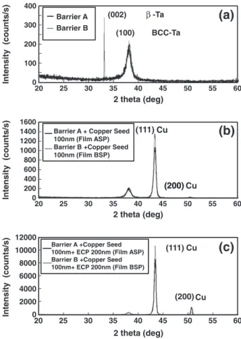
In order to investigate the effect of barrier on the chemical mechan-ical polishing behavior of copper, two barrierfilms, Barrier A and Barrier B, were prepared at essentially the same time with 15 nm thickness. The other four samples were deposited with 100 nm thick copper seed and 200 nm thick electroplating copper on Barrier A and Barrier B, respec-tively. X-ray diffraction was used to determine the textures of these six samples, as shown inFig. 1a to c, respectively. InFig. 1a, it reveals that Barrier B got very strongβ-Ta (002) and bcc-Ta (110) textures. Compared with Barrier B, it is found that Barrier A had the comparable intensity of bcc-Ta (110), but lacked forβ-Ta (002) peak. Stavrev et al. [17]mentioned that the interstitially incorporation of small numbers
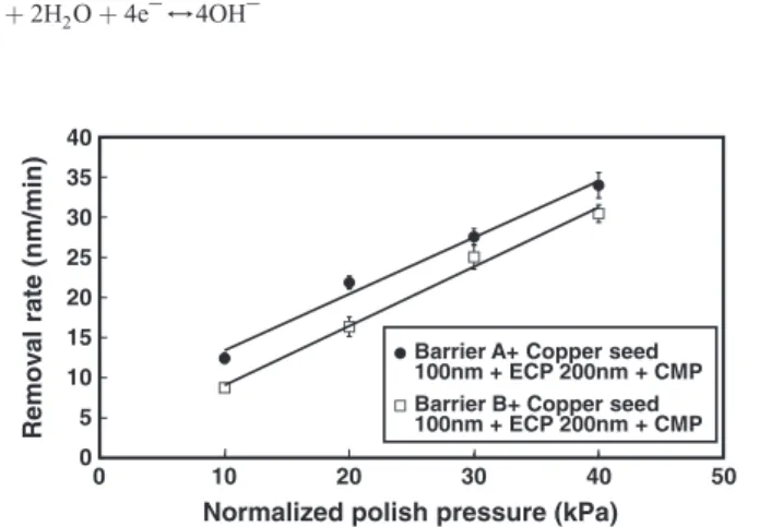
N atoms into Tafilms causes the crystal structure change from β-Ta and bcc-Ta to pure bcc-Ta.Fig. 1b shows that Film BS (sputtered copper seed layer deposited on Barrier B) had stronger (111) copper texture than that of Film AS (sputtered copper seed layer deposited on Barrier A). Based on the heteroepitaxial growth study of copper onβ-Ta men-tioned by Kwon et al.[9], the (111) texture growth of the copperfilm is enhanced when the underlying barrier layer is (002) β-Ta by a pseudohexagonal atomic arrangement. This strong (111) copper seed orientation developed an intense (111) texture for the sequential cop-per electroplating layer of Film BSP (electroplating copcop-per deposited on Film BS), as shown inFig. 1c. According to the research of Hara et al.[18], the (111) texture of the electroplating copper layer is mainly determined by that of the underlying seed layer. Dow et al.[19] demon-strated that the intensity ratio of (111)/(200) texture is in good agree-ment between electroplating and seed layer.Fig. 1c also shows the same phenomenon that Film BSP had higher (111)/(200) ratio. In the previous studies [12,13], copper polished surface with high (111)/ (200) ratio has strong chemical resistance. For face-centered cubic (FCC) copper thinfilm, (111) texture should exhibit stronger chemical resistance than other planes because (111) is the closest packed plane. Chemical properties of copper surface play an important role in the CMP process. The mechanism of copper CMP is mechanical abrasion followed by chemical dissolution of the abraded material. Xu and Liang[20]proposed that copper removal mechanism is based on the cy-clic sequence of copper passivation followed by the mechanical removal of the passive layer due to abrasion. During CMP, hydrogen peroxide (oxidizing agent) and glycine (complexing agent) form a porous and soft surface layer leading to high removal rate. Thus, the copper removal rate is a useful index to study the CMP behavior.Fig. 2shows the corre-lations between the CMP applied pressures and the relative copper CMP
(002) (100) β -Ta BCC-Ta Intensity (counts/s)
(a)
Barrier A Barrier B 20 25 30 35 40 45 50 55 60 400 300 200 100 0 2 theta (deg) (200) (200) Cu (111) Cu Intensity (counts/s)(b)
20 25 30 35 40 45 50 55 60Barrier A + Copper Seed 100nm (Film ASP) Barrier B +Copper Seed 100nm (Film BSP) 1600 1400 1200 800 600 400 0 1000 200 2 theta (deg) (200) Cu (111) Cu Intensity (counts/s)
(c)
20 25 30 35 40 45 50 55 60 2 theta (deg)Barrier A +Copper Seed 100nm+ ECP 200nm (Film ASP) Barrier B +Copper Seed 100nm+ ECP 200nm (Film BSP) 12000 10000 8000 6000 4000 2000 0
Fig. 1. X-ray diffraction texture patterns for compositefilms for (a) the barrier layers, (b) the barrier and sputtered copper seed layers, (c) the barrier, sputtered copper seed, and electroplated copper layers, respectively.
removal rates of Film ASP and Film BSP, respectively. It reveals that no matter what the textures of the barrier layer and copper layer were, the copper removal rates increased with increasing applied polish pres-sure. This matches the Preston's equation that describes the relation-ship between the polish removal rate and the polish pressure[10]. The increase of pressure raises temperature between slurry and copper surface to naturally speed up etching and passivation layer CuOx forma-tion. High etching rate and porous CuOxinterface, which can reduce frictional force between pad, slurry and wafer surface, cause linear rela-tionship between removal rate and applied pressure[21]. It also can be seen inFig. 2that the removal rate of copper deposited on Barrier A was higher than that deposited on Barrier B which had strong (002)β-Ta texture. This can be explained by the orientation difference shown in
Fig. 1c. Copper deposited on Barrier B had high (111)/(200) ratio with
stronger chemical resistance because of denser structure of (111) plane. Jindal and Babu[22]reported that the CMP removal mechanism of copperfilm in slurries is to form a porous surface layer leading to higher removal rate and to reduce friction thus softening the surface layer. Denser structure reduced the chemical effect when polished and made copper not easy to be removed.
Hydrogen peroxide is commonly used as an oxidizer in commercial copper CMP slurries [23]. An aqueous solution containing 0.001 M Na2SO4solution with 0.2 wt.% H2O2was prepared to investigate the cor-rosion behaviors of copperfilms ASP and BSP by the measurement of potentiodynamic polarization curves in this study.Fig. 3displays the stat-ic potentiodynamstat-ic polarization behaviors for Film ASP and Film BSP. The results reveal that the corrosion current density of Film BSP (79μA/cm2) was lower than that of Film ASP (142μA/cm2). Lower corrosion current means better chemical resistance. This implies that the compositefilm (BSP) with strong (002)β-Ta underlying barrier layer and (111) copper orientation had relatively high chemical resistance against surface reac-tion with slurry, which caused lower copper CMP removal rate as shown inFig. 3. Furthermore, the data inFig. 3also indicated that the pas-sivefilm formed on Film BSP might be more passive than that on Film ASP in the solution containing H2O2. When scanning in the positive potential direction, the formation of passivefilm in both Film ASP and Film BSP was observed based on the existence of a substantial peak in the anodic re-gion. It appears that the passive layer started to grow for Film BSP around 0.51 V and Film ASP around 0.55 V, respectively, since the current density started to rise slower as the potential increased. The passive current den-sities of bothfilms were significantly different, indicating that Film BSP was protected well compared to Film ASP at the region.
Several studies have mentioned that copper reacts in the presence of H2O2or O2can form a weak passivation layer. The most likely cath-ode reductions may include oxygen reduction and decomposition of
H2O2[24,25]:
O2þ 2H2O þ 4eP↔4OHP ð1Þ
H2O2þ 2eP↔2OHP: ð2Þ
Anodic reactions depending on the electrode potentials displayed
inFig. 4may include active dissolution of copper and oxidation of
cu-prous oxide. Both reactions compete with the variation of sweep po-tential. While potential swept just after the corrosion potentials of Film ASP and Film BSP, the dominated anodic reaction was Eq.(3) as shown below, dissolution of copper. Therefore, current density in-creased with raising potential.
Cu→Cu2þþ 2eP
ð3Þ
2Cu þ H2O→Cu2O þ 2Hþþ 2eP ð4Þ
Furthermore, as potential scanning close to 0.51 V or 0.55 V, the turning point of current density of Film BSP and Film ASP, the domi-nated anodic reaction changed to Eq.(4), which is the oxidation of cu-prous oxide. Because the passive layer formed on copper surface and even protected surface probability, current density started to rise slowly with increasing potential. The existence of passivation region in bothfilms also implies that the oxidation occurs on copper surface without applying potential. Previous research also detected oxides formed on copper immersed in H2O2based slurries when no electric field was applied[26].
In order to differentiate the passive potential for bothfilms, the chronoamperometric test at 0.3 V, which was in the narrow passive potential range, was carried out onfilm A and film B in the H2O2 so-lution. The variation of current densities with time during the test was recorded simultaneously as well, as shown inFig. 4. The current density of Film ASP decayed from 89μA/cm2to 41μA/cm2speedily
0 5 10 15 20 25 30 35 40 0 10 20 30 40 50
Normalized polish pressure (kPa)
Remov
al rate
(nm/min)
Barrier A+ Copper seed 100nm + ECP 200nm + CMP Barrier B+ Copper seed 100nm + ECP 200nm + CMP
Fig. 2. The correlations between the CMP applied pressures and the relative copper CMP removal rates of Film ASP and Film BSP.
-1.2 -1 -0.8 -0.6 -0.4 -0.2 0 0.2 0.4 0.6 0.8 1 1.2
1.E-07 1.E-06 1.E-05 1.E-04 1.E-03 1.E-02
Current density (µA/cm2)
Potential (V
v
s
SSCE)
Barrier A + copper seed 1k + ECP 2k (Film ASP)
Barrier B + copper seed 1k + ECP 2k (Film BSP)
Fig. 3. The static potentiodynamic polarization behavior for Film ASP and Film BSP.
Barrier A + Copper Seed 100nm + ECP 200nm (Film ASP)
Barrier B + Copper Seed 100nm + ECP 200nm (Film BSP) 0 20 40 60 80 100 Current density (µA /c m 2) 0 5 10 15 20 25 30 Time (Sec)
Fig. 4. The change of current densities with time of Film ASP and Film BSP at applying potential 0.3 V in the H2O2solution.
437 Y.-S. Wang et al. / Thin Solid Films 529 (2013) 435–438
while that of Film BSP always kept almost constant and was lower than Film ASP. Higher current density that represented more electron exchange occurred on the sample surface. The result indicates that the passivefilm formed on Film ASP could offer more paths than Film BSP to induce oxidizer contacting fresh Cu surface so that oxidation–reduction reaction occurred on Film ASP easier than that on Film BSP. This also consisted to the result of corrosion current density that was displayed
inFig. 3.
From the above study, it reveals that strong (002)β-Ta underlying layer produced strong (111) copper orientation, which has lower copper removal rate and better chemical corrosion resistance. This is because the (111) texture is the closest packed plane in the copper FCC structure, which means densefilm structure. Thus, the film struc-ture density is an important factor for copper CMP behavior under-standing. Denser structure can resist chemical attack and reduce the removal rate. Currently several techniques are used to analyzefilm quality, such as X-ray diffraction, scanning electron microscope, and transmission electron microscope. Most of them take a long time for sample preparation and tool operation. How to analyzefilm density with higher efficiency is worth studying in next paper.
4. Conclusion
This study indicated the correlation between the barrier texture and copper corrosion behavior. X-ray diffraction analysis reveals that if the texture of underlying barrier layer was (002)β-Ta, the sub-sequent copper layer got strong (111) orientation. This strong (111) texture had high chemical resistance ability, which was proved by the results of copper removal rate after the chemical mechanical planarization and the static potentiodynamic polarization analysis. The removal rate measurement result, which matched the Preston's correlation under different polish pressure, shows that the removal rate of copper plated on strongβ-Ta was low; this is because copper plated on strongβ-Ta has high (111)/(200) ratio with stronger chem-ical resistance because of the closest packed structure of copper (111) plane. Denser structure reduced the chemical effect when polished and made copper not easy to be removed. The measurement of potentiodynamic polarization for corrosion behavior, which in an aqueous solution containing 0.001 M Na2SO4solution with 0.2 wt.%
H2O2, demonstrates that the corrosion current density offilm plated on (002)β-Ta (79 μA/cm2) was lower than that on the barrier with-outβ-Ta (142 μA/cm2), hence better chemical resistance against the surface reaction with slurry. This was coincidence with the result of the chronoamperometric test at 0.3 V that the passivefilm formed on thefilm with (002) β-Ta barrier was more passive.
References
[1] C. Ryu, A.L.S. Loke, T. Nogami, S.S. Wong, Proceedings of the IEEE International Re-liability Physics Symposium, 1997, p. 201.
[2] C. Ryu, K.W. Kwon, A.L.S. Loke, H. Lee, T. Nogami, V.M. Dubin, R.A. Kavari, G.W. Ray, S.S. Wong, IEEE Trans. Electron Devices 46 (6) (1999) 1113.
[3] E.M. Zielinski, R.P. Vinci, J.C. Bravman, J. Appl. Phys. 76 (8) (1994) 4516. [4] S.S. Wong, C. Ryu, H. Lee, A.L.S. Loke, K.W. Kwon, S. Bhattacharya, R. Eaton, R.
Faust, B. Mikkola, J. Mucha, J. Ormando, IEEE, International Interconnect Technol-ogy Conference, 1998, p. 107.
[5] Q.-T. Jiang, R. Faust, H.R. Lam, J. Mucha, IEEE, International Interconnect Technol-ogy Conference, 1999, p. 125.
[6] J. Chen, S. Parikh, T. Vo, S. Rengarajan, T. Mandrekar, P. Ding, L. Chen, R. Mosely, IEEE, International Interconnect Technology Conference, 2002, p. 185. [7] T. Hara, Electrochem. Solid-State Lett. 6 (5) (2004) C57.
[8] S. Balakumar, R. Kumar, Y. Shimura, K. Namiki, M. Fujimoto, H. Toida, M. Uchida, T. Hara, Electrochem. Solid-State Lett. 7 (4) (2004) G68.
[9] K.W. Kwon, C. Ryu, R. Sinclair, S.S. Wong, Appl. Phys. Lett. 71 (21) (1997) 3069. [10] J.M. Steigerwald, S.P. Murarka, R.J. Gutmann, Chemical Mechanical Planarization
of Microelectronic Materials, John Wiley & Sons, Inc., New York, 1997 chapter 4. [11] W.-T. Tseng, Y.L. Wang, J. Electrochem. Soc. 144 (1997) L15.
[12] J.Y. Lin, C.C. Wan, Y.Y. Wang, H.P. Feng, J. Electrochem. Soc. 154 (2007) D139. [13] J.Y. Lin, Y.Y. Wang, C.C. Wan, H.P. Feng, M.Y. Cheng, J. Electrochem. Soc. 10 (2007)
H23.
[14] D.A. Jones, Principles and Prevention of Corrosion, 2nd ed., Prentice-Hall, Inc., Upper Saddle River, NJ 07458, 1996 Ch3.
[15] M. Stern, A.L. Geary, J. Electrochem. Soc. 104 (1957) 56. [16] J.H. Wang, L.J. Chen, J. Vac. Sci. Technol. B 20 (4) (2002) 1522. [17] M. Stavrev, D. Fischer, J. Vac. Sci. Technol., A 17 (3) (1999) 993.
[18] T. Hara, K. Sakata, Y. Yoshida, Electrochem. Solid-State Lett. 5 (3) (2002) C41. [19] W.P. Dow, H.S. Huang, Z. Lin, J. Electrochem. Soc. 6 (2003) C134.
[20] G. Xu, H. Liang, J. Electrochem. Soc. 151 (2004) G688. [21] K.W. Chen, Y.L. Wang, J. Electrochem. Soc. 154 (2007) H41. [22] A. Jindal, S.V. Babu, J. Electrochem. Soc. 151 (2004) C709.
[23] S.V. Babu, K.C. Cadien, H. Yano (Eds.), Chemical–Mechanical Polishing 2001: Ad-vances and Future Challenges, Materials Research Society, Warrendale, PA, 2001. [24] C.M. Miller, R.L. Valentine, Water Res. 33 (1999) 2805.
[25] T. Du, D. Tamboli, V. Desai, Microelectron. Eng. 69 (2003) 1.
[26] J. Hernandez, P. Wrschka, G.S. Oehrlein, J. Electrochem. Soc. 148 (2001) G389. 438 Y.-S. Wang et al. / Thin Solid Films 529 (2013) 435–438