420 JOURNAL OF DISPLAY TECHNOLOGY, VOL. 7, NO. 8, AUGUST 2011
Gap-Type a-Si TFTs for Backlight Sensing
Application
Ya-Hsiang Tai, Lu-Sheng Chou, Yan-Fu Kuo, and Shao-Wen Yen
Abstract—In this paper, a new photo device are proposed using gap-typed hydrogenated amorphous silicon (a-Si:H) thin-film transistors (TFTs) as backlight sensing circuits. The system em-ploys gap type a-Si TFTs, which has higher photo sensitivity, to sense illumination and increase device dynamic range. Meanwhile, the system with local dimming technologies could attain the pur-pose for self-adjusting function. It is expected that the integration of this sensing system onto the panel can be implemented without extra process development. Furthermore, the photo leakage char-acteristics of a-Si TFTs after optical stress are investigated and the corresponding calibration method is proposed to reduce the error in sensing the illumination intensity. This approach would provide the possibility for the sensors array to be integrated into the pixel with the same a-Si TFT device.
Index Terms—Amorphous thin-film transistor (TFT), gap-type, light sensor, circuits.
I. INTRODUCTION
H
YDROGENATED amorphous silicon (a-Si:H) thin-film transistors (TFTs) receive extensive application in active matrix liquid crystal display (LCD) and sensor applications due to its high photo sensitivity and ease of deposition across large area substrates [1]–[3]. Sensor on panel is one of the value-added functions for display panel. Some applications using a-Si TFTs, such as local dimming technology, which can adjust backlight intensity depending on the feature of each frame, were also reported to lower power consumption and improve visibility [4], [5]. However, the LED backlight modules degraded divisionally and its light emission could be nonuniform in large panels after long time operation [6]–[9]. Therefore, in this paper, we propose a backlight sensor system employing novel photo device to sense accurate illumination intensity. The conventional a-Si TFTs, adopting the bottom gate structure, can effectively detect the front light [10], [11], but can hardly be used to sense the backlight because of the shielding of the gate metal. To reduce the effect of gate metal shielding,Manuscript received January 29, 2010; revised May 24, 2010; ac-cepted March 14, 2011. Date of current version June 15, 2011. This work was supported by the National Science Council, Republic of China, under NSC97-2218-E-009-005, and was supported in part by the MOE ATE program and MOEA Technology Development Academia Project 96-EC-17-A-07-S1-046.
Y.-H. Tai and S.-W. Yen are with the Department of Photonics & Display Institute, National Chiao Tung University, Hsinchu 30010, Taiwan (e-mail: yhtai@mail.nctu.edu.tw).
L.-S. Chou and Y.-F. Kuo are with the Department of Photonics & Institute of Electro-Optical Engineering, National Chiao Tung University, Hsinchu 30010, Taiwan.
Color versions of one or more of the figures are available online at http:// ieeexplore.ieee.org.
Digital Object Identifier 10.1109/JDT.2011.2135838
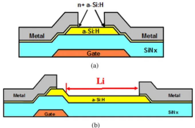
Fig. 1. Cross-section view of a-Si TFTs with (a) conventional and (b) gap-type device structures.
a non-conventional structure, namely the gap type structure, is proposed as the sensing device and it has the same fabrication process as the conventional a-Si:H TFTs. Thus, the light sensor can be integrated in panel without changing the mask number and extra cost. Moreover, since the circuit performance varies with device variation cause non-uniformity of display image, we take further steps by demonstrating embedded backlight sensors with a-Si TFTs and estimating the influence from different device variation. Meanwhile, we propose sensing circuits directly using a-Si TFTs which identically fabricated with the pixel TFT. This proposed circuit is capable of sensors array integration to a-Si TFTs.
II. DEVICECONFIGURATION ANDFABRICATION
In this experiment, the new sensing devices take advantage of the same a-Si TFTs process. The device process flow is described as followed. Firstly, the gate metal was deposited and patterned on the glass substrates. Then, silicon nitride (SiNx, 3500 ), a-Si:H, and n a-Si:H films, were successively deposited in a plasma-enhanced chemical vapor deposition (PECVD) system. Subsequently, the source/drain electrodes were formed and defined, followed by the n a-Si:H region with length (L) of 5 m between the source/drain electrodes was etched off by a reactive ion etch. Finally, a passivation layer was used to cap the channel region. The cross-section view of conventional and gap-type structure TFTs are shown in Fig. 1(a) and (b). The only difference between two device structures is that the gap-type device structure has a gap region between the source/drain metal and the gate metal [12]. Such configuration is less light sensitive than the gap region placed on the source side. Therefore, in this work, gate-near-source TFTs are used to be the photo sensor device. The gap size of
Fig. 2. I –V transfer characteristics under different illumination conditions for: (a) conventional and (b) gap-type device structures.
the new structures, existing between bottom gate metal and one of top drain metal, is expressed as Li.
III. RESULTS ANDDISCUSSION
A. Illumination Effect of Device
Fig. 2(a) and (b) shows the conventional and gap-type TFTs transfer characteristics in the dark as well as irradiated at six different levels of illumination from the backlight at
V. Since the gate metal shielded all the possible backlight which could illuminate on active layer, it can be seen obviously that the conventional TFT does not have any photo sensitivity. On the other hand, in aspect of gap-type TFTs, it has signifi-cantly higher photosensitivity not only in off region but also in on region. This wide dynamic range is obtained by gap region forms the higher channel resistance, which leads to the lower dark current, and creates additional photo-generated carriers, which leads to the higher photo current.
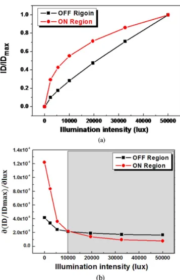
Moreover, we take further steps to compare both operating regions for backlight sensing. Fig. 3(a) shows the on and off drain current of gap-type TFT with different backlight inten-sity. Device operated in on or off region is decided by gate voltage which is higher or lower than threshold voltage, respec-tively. (The gate voltages of on and off regions are 10 V and 10 V, respectively.) However, in this way the photo sensi-tivity cannot be compared directly because of the different cur-rent levels, respectively. Therefore, the normalized drain curcur-rent is differentiated with the backlight intensity and its behavior versus the illumination intensity is shown in Fig. 3(b). In this
Fig. 3. Comparison of photo sensitivity between on and off region (a) after normalization and (b) after differentiation.
way the photo-sensitivity for the on and off region is distin-guished under different back light intensities. It should be noted that there is an intersection point under 10000 lux illumination. The sensing device operated in the on region has higher photo-sensitivity for the backlight intensity under 10000 lux. On the other hand, as the back light intensity larger than 10000 lux, de-vice operated in the off region has better photosensitivity. Base on the real panel operation consideration, backlight intensity which passes through the polarizer and then reaches the TFT array layer would not be over 10000 lux. Meanwhile, the op-erated current level in on region is higher than in off region. It can be read out easily and therefore the optical signal-to-noise ratio (SNR) can be increased. On the basis of these reasons, it would be beneficial to operate the sensing device in on region for sensing backlight.
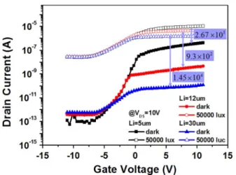
The gap-type TFTs which have active layer between the bottom gate metal and the drain metal can detect the backside illumination. To analyze the illumination effects in detail, photo devices with different gap lengths were fabricated and tested, as shown in Fig. 4. It reveals that the photosensitivity is larger in on region as the gap increases. The characteristics of those devices in the dark are very different, which makes it difficult to compare the effect of illumination on them. Consequently, considering the easiness of the readout system and the pixel
422 JOURNAL OF DISPLAY TECHNOLOGY, VOL. 7, NO. 8, AUGUST 2011
Fig. 4. Photosensitivity under various channel length of gap-type a-Si:H TFT.
Fig. 5. Relation betweenI and open ratio.
aperture ratio, the proper fixed gap length must be evaluated for TFT design.
Moreover, we design different gap lengths of floating gate TFT structures to analyze the relation between the gap and the photo effect. The function of the extra gate is to shield off backlight illumination. If the area of gap is shielded S% from backlight illumination with the floating gate, then the index “Open{\_}ratio” would be open{\_}(100-S)%. Fig. 5 shows the relation between the drain current and open{\_}ratio (with the floating dual gate structures shown in insert). As the figure shows, is proportional to the open{\_}ratio. It reveals that the photo effect is proportional to the illuminated area of the gap in the gap-type device.
B. Sensing Circuits and Its Driving Schemes
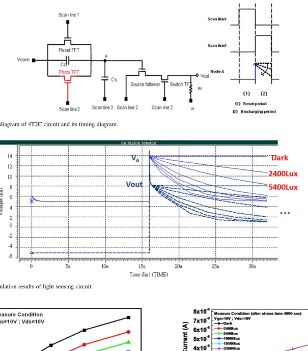
Based on the results mentioned above, a new light sensing circuit with only one readout bus but no extra bus is proposed. The schematic diagram of 4T2C circuit and its timing diagram are shown in Fig. 6. The sensing part is composed of a reset TFT, a photo TFT, and two capacitors, and . The readout part is composed of a source follower and a switch TFT.
The operating principles can be described as two periods, as shown in Fig. 6. In the reset period, scan line1 signal ( 10 V to 10 V) becomes “high,” and the reset TFT is turned on. Thereby, the voltage of node A is charged to (5 V). In the dis-charging period, the scan line1 signal becomes “low,” reset TFT is turned off. Meanwhile, the scan line 2 signal becomes “high,”
the photo TFT is operated in ON region. The backlight is turned on during the discharging period. At the same time, the voltage of node A rise to a relatively high voltage to owing to the couple effect from the voltage changing of scan line 2 through . Then, the photo current, which is determined by the inten-sity of the illumination, drained away through the photo TFT. The voltage of node A would be discharged by the photo cur-rent of photo TFT, and then voltage change at node A can be fol-lowed by source follower, and readout through switch TFT line by line. The is especially added to divide voltage of node A to a proper for photo TFT when coupling happened. Mean-while, it can make sure the voltage at node A be lower than the drain voltage of source follower ( , on in our case) for its prop-erly working. Fig. 7 shows the SPICE simulation results of light sensing circuit. The simulation method is modified according to illuminated output characteristics of device. Meanwhile, the different current sources and resistors in parallel are to represent the different photo currents of TFT. The illumination intensity can be monitored by the slope of the discharging voltage.
IV. DEVICESVARIATION
A. Staebler-Wronski (SW) Effect
In real applications, the device variation is always an im-portant issue of TFTs. It is clear that device-to-device unifor-mity must be controlled for circuit application. Several possible sensing error factors like device uniformity, temperature, and in-stability of a-Si must be considered. However, from the study of photo current response of a-Si:H TFTs, Staebler-Wronski (SW) effect is a dominant influence to light sensing [13]–[15]. The predominant explanation of the effect is that the illumination leads to the creation of additional metastable states in the band gap of the amorphous silicon, by breaking the weak bounds of the hydrogen atoms to the silicon, which decreases the lifetime of excess carriers and thus reduces the photoconductivity.
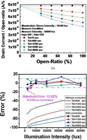
To study the SW effect, we use 19160 lux backlight to illu-minate the device, and the stress time is from 0 to 4800 s. Fig. 8 shows the result of optical stress. It can be observed that the current degrades obviously with stress time increasing. In addi-tion, the exposure time of the measurements (15 s) is much less than light stress time (600–4800 s). For this reason, we neglect the degradation resulted from measurements. As compared with other error factors, SW effect is very serious. If it is not cali-brated, the device cannot be applied at all. Thus in this work, a method will be proposed to solve this issue. Before explaining the calibration method, we mentioned the is propor-tional to the illuminated area of gap. After optical stress, the device with larger open-ratio will suffer from worse stress be-cause the gap area is larger. The different stress levels will result in the nonlinear dependence of photo current on the operation as shown in Fig. 9.
B. Calibration Method of Staebler-Wronski Effect
Before introducing the calibration method, we define the ID/Open-ratio as the new index. The ID/Open-ratio versus open-ratio before stress is shown in Fig. 10(a). It can be found that the ID/Open-ratio is independent of open-ratio before stress. Since the device’s degradation level associates with illuminated intensity, stress time as well as illuminated area, it implies that the larger open-ratio structure will degrade
Fig. 6. Schematic diagram of 4T2C circuit and its timing diagram.
Fig. 7. SPICE simulation results of light sensing circuit.
Fig. 8. Measured current of a-Si TFT under optical stress.
more. Fig. 10(b) shows ID/Open-ratio behavior of the stressed devices. The one with 100% open ratio degrades most. The smaller open-ratio structure subjects to smaller influence from SW effect. The first idea coming to mind is to find the open-0% structure which means it will not be stressed by backlight. Since there is no open-0% structure of gap-type TFT, which will be-come conventional TFT and insensitive to backlight, it could
Fig. 9. Relation betweenI and open ratio after optical stress.
be alternatively achieved by extrapolating the ID/Open-ratio behavior with different open ratios. For example, Fig. 11(a) shows the result of extrapolation. A formula in the form of by OriginPro software is used to extrapolate the case of 0% stress.
After the calibration, the maximum error, shown in Fig. 11(b), can be reduced to about 13.6%. Here the “Error” is defined as
[(Lux -Lux Lux ]. For the case without the
cali-bration, the value, Lux , can be evaluated from the mea-sured drain current of the gap-type TFT. The initial relation-ship between illuminations and drain current of the gap-type
424 JOURNAL OF DISPLAY TECHNOLOGY, VOL. 7, NO. 8, AUGUST 2011
Fig. 10. ID/Open-ratio versus open-ratio: (a) before and (b) after optical stress.
TFT can be obtained by the behavior shown Fig. 2. For the proposed calibration, the drain current of open-0% structure of gap-type TFT can be obtained by extrapolation to evaluate the value Lux based on the illuminated characteristics of Fig. 10(a). In the Fig. 11(b), the “without correction” curves present the errors produced by SW effect on Open-100% gap-type TFTs, and the “with correction” curves present the errors modified by the proposed calibration method. In the proposed method, the different open-ratio gap-type TFTs will be imple-mented in neighboring sensing pixels to ensure these gap-type TFTs are exposed to almost equal illumination intensity and our calibration can be thus executed. This result indicates that the calibration method is very effective to lower the influence of SW effect.
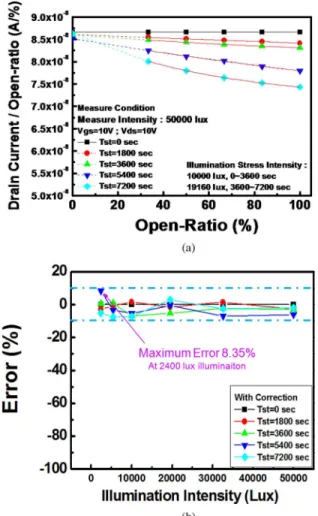
In reality, the backlight intensity is not always fixed. There-fore, it would be of practical interest to verify the feasibility of the aforementioned calibration method under changed back-light stress. In the following study a two-step backback-light illu-mination is used. From 0 to 3600 s, the devices are stressed by l0000 lux backlight. And in the following 3600 s, the de-vices continue to be stressed by l9160 lux backlight. Because of the different stressed intensities, the curves present two dif-ferent degradation rates as shown in Fig. 12. As for the cali-bration method, Fig. 13(a) shows the characteristics stressed by the two-step light intensities and illustrates the same trend as Fig. 11(a), which is stressed under the fixed backlight intensity. The same proposed method is used to calibrate the influence of SW effect. The error in different stress condition is shown in Fig. 13(b). It can be seen that the proposed calibration method
Fig. 11. (a) Calibration of SW effect and (b) error analysis with/without calibration.
Fig. 12. Different stress intensities, the curves present two different degradation rates.
still can calibrate the SW effect effectively under the changing backlight illuminating situation.
V. CONCLUSION
In this paper, a non-conventional TFT, namely the gap-type structure, is proposed to be the backlight sensing device. The ad-vantage of such device is its higher current level and good pho-tosensitivity in the on region, which is beneficial to sense light intensity. A light sensing circuit is proposed to integrate into pixel without any extra power bus. Moreover, the possible fac-tors which would affect the sensing accuracy are discussed and it is found that the SW effect is the biggest issue. It will cause
Fig. 13. (a) Calibration of SW effect and (b) error analysis under two-step stress intensities.
the malfunction of the sensor circuit or lead to large error in sensing the back light intensity. Therefore, a calibration method is proposed to reduce the influence of SW effect by extrapo-lating. After such calibration the error can be reduced to below 10%, which may be acceptable in real application. Such ap-plication method is found also applicable under the changing back light intensity. It reveals that the proposed device structure along with the calibration method could be applicable in real back light sensing application.
REFERENCES
[1] M. Katayama, “TFT-LCD technology,” Thin Solid Films, vol. 341, no. 1–2, pp. 140–147, Mar. 1999.
[2] B. D. Choi and O. K. Kwon, “Stepwise data driving method and circuits for low-power TFT-LCDs,” IEEE Trans. Consum. Electron., vol. 46, no. 4, pp. 1155–1160, Nov. 2000.
[3] C. C. Lai and C. C. Tsai, “Backlight power reduction and image con-trast enhancement using adaptive dimming for global backlight appli-cation,” IEEE Trans. Consum. Electron., vol. 54, no. 2, pp. 669–674, Nov. 2008.
[4] M. Anandan, “LED backlight: Enhancement of picture quality on LCD screen,” in SID’06 Dig., 2006, pp. 130–134.
[5] M. Zeiler, L. Plötz, W. Schwedler, and H. Ott, “Highly efficient LED backlight solutions for large LCDs,” in Dig. Tech. Papers Workshop
Active-Matrix Flat Panel Displays and Devices, 2005, p. 57.
[6] C. Hoelen and G. Harbers, “LCD backlighting with high luminescent colored light emitting diodes,” in SID’01 Dig., 2001, p. LS-9. [7] G. Harbers and C. Hoele, “High performance LCD backlighting using
high intensity Red, Green and Blue light emitting diodes,” in SID’01
Dig., 2001, pp. 702–705.
[8] G. Harbers, W. Timmers, and W. Sillevis-Smitt, “LED backlighting for LCD-HDTV,” J. SID, vol. 10, no. 4, pp. 347–350, 2002.
[9] R. S. West, H. Konijn, W. Sillevis-Smitt, S. Kuppens, N. Pfeffer, Y. Martynov, Y. Takaaki, S. Eberle, G. Harbers, T. W. Tan, and C. E. Chan, “High brightness direct LED backlight for LCD-TV,” in SID’03
Dig., 2003, pp. 1262–1265.
[10] W. den Boer, A. Abileah, P. Green, T. Larsson, S. Robinson, and T. Nguyen, “Active matrix LCD with integrated optical touch screen,” in
SID’03 Dig., 2003, pp. 1494–1497.
[11] A. Abileah, W. den Boer, T. Larsson, T. Baker, S. Robinson, R. Siegel, N. Fickenscher, B. Leback, T. Griffin, and P. Green, “Integrated optical touch panel in a 14.1 AMLCD,” in SID’04 Dig., 2004, pp. 1544–1577. [12] S. M. GadelRab and S. G. Chamberlain, “The source-gated amorphous silicon photo-transistor,” Trans. on Electron. Devices, vol. 44, no. 10, pp. 1789–1794, Oct. 1997.
[13] M. Vanecek, A. Poruba, A. Fejfar, and J. Kocka, “Direct measurement of the deep defect density in thin amorphous silicon films with the ab-solute constant photocurrent method,” Jpn. Soc. Appl. Phys., vol. 78, no. 10, pp. 6203–6210, 1995.
[14] T. Kruger, “On the origin of the Staebler-Wronski effect,” J. Appl.
Phys., vol. 99, no. 6, p. 063509, Mar. 2006.
[15] L. Eglseer, S. Horvat, and H. Kroha, “Study of the long-term behavior of the sensitivity of amorphous silicon photo detectors under illumina-tion,” in Eur. Symp. on Semiconductor Detectors, Nov. 2006, vol. 568, no. 1, pp. 18–21.
Ya-Hsiang Tai received the B.S. and Ph.D. degrees
in electronic engineering from National Chiao Tung University, Hsinchu, Taiwan, , in 1990 and 1996, re-spectively.
He became a member of Industrial Technology Research Institute/Electronics Research & Service Organization and the TFT LCD development as a panel designer. He joined the project of low temperature polycrystalline silicon (LTPS) thin-film transistor (TFT) development in Prime View In-ternational in 2000. In 2001, he entered Toppoly Optoelectronics Corporation, to lead the team of LTPS TFT LCD panel design. He joined the faculty of National Chiao Tung University in 2003, where he is currently an associate professor in the Department of Photonics and Display Institute. His current research emphases are in the areas of TFT device physics, active matrix display panel design, and system on panel.
Lu-Sheng Chou received the B.S. degree in physics
from National Sun Yat-Sen University, Taiwan, in 2008, and is currently working toward the Ph.D. degree in electro-optical engineering in National Chiao Tung University, Taiwan.
His current research interests include the sensor and applications of a-Si and a-IGZO TFTs.
Yan-Fu Kuo received the B.S. degree in physics
from National Sun Yat-Sen University, Taiwan, in 2002, the M.S. degree in electro-optical engineering in National Chiao Tung University, Taiwan, in 2004, where he is now working toward the Ph.D. degree.
His current research interests include the sensor and applications of low-temperature poly-Si TFTs.
Shao-Wen Yen received the B.S. degree in electrical engineering from National
Central University, Taiwan, in 2007.