Thin Solid Films 447 – 448(2004) 524–530
0040-6090/04/$ - see front matter䊚 2003 Elsevier B.V. All rights reserved. doi:10.1016/j.tsf.2003.07.028
CMP of ultra low-k material porous-polysilazane
(PPSZ) for interconnect
applications
T.C. Chang
a,b,*, T.M. Tsai , P.T. Liu , C.W. Chen , S.T. Yan , H. Aoki , Y.C. Chang , T.Y. Tseng
c d c c e e c Department of Physics and Institute of Electro-Optical Engineering, National Sun Yat-Sen University, 70 Lien-hai Rd., Kaohsiung, Taiwan, aROC
Center for Nanoscience & Nanotechnology, National Sun Yat-Sen University, Kaohsiung, Taiwan, ROC b
Institute of Electronics, National Chiao Tung University, Hsin-Chu, Taiwan, ROC c
National Nano Device Laboratory, 1001-1 Ta-Hsueh Rd., Hsin-Chu 300, Taiwan, ROC d
Life Science and Electronic Chemicals Division, Clariant Corp., Bunkyo Green Court 2-28-8 Honkomagome, Bunkyo-ku, Tokyo 113-8662, e
Japan
Abstract
In this article, we investigated the impact of chemical mechanical polishing(CMP) on an ultra low dielectric constant (ultra low-k) material Porous-Polysilazane (PPSZ) with slurries of metal polishing during interconnect manufacture process. Since the CMP processing of metals such as TaN and Cu are inevitable steps for interconnect fabrication, we have utilized two types of slurries (marked as TaN and Cu slurries) to evaluate their effects on the dielectric properties of PPSZ films. Electrical and material analyses have shown surface planarity and dielectric properties of PPSZ films will not be degraded during these metal CMP processes. This indicates that the ultra low-k PPSZ films are promising for inter-level dielectric(ILD) applications in ultra large-scale integrated circuits(ULSI) technology.
䊚 2003 Elsevier B.V. All rights reserved.
Keywords: Chemical mechanical polishing; Ultra low-k; Porous-polysilazane films; Copper
1. Introduction
Shrinking device dimensions associated with ultra large scale integrated circuits is highly effective in achieving high speed performance and in increasing yields at lower cost per chip. In order to assure the performance of the high-speed circuits, continuous efforts have been devoted for incorporating copper or
low-dielectric constant(low-k) materials into multilevel
interconnections for reducing the major part of circuit delay, cross talk, and power consumption w1–3x. For
integrating Cu and low-k materials into integrated
cir-cuits (ICs), the damascene technique w4,5x (shown in
Fig. 1) with chemical mechanical polishing (CMP) w6,7x
is the most suitable approach towards using copper in a multilevel metallization scheme. Furthermore, it is reported that Cu easily diffuses into most low-k materials
during interconnect manufacture processes and reliability testing w8,9x. Therefore, the barrier metal such as TaN
*Corresponding author. Tel.: 7-5252000x3708; fax: q886-7-5253709.
E-mail address: [email protected](T.C. Chang).
has been extensively used between Cu and low-k
mate-rials to protect Cu from diffusing into low-k materials.
The polishing processes, for removing excess copper or TaN on damascene structures and associated with a resultant flat surface w10,11x is crucial for building-up multilevel interconnects scheme. Although a lot of studies have been focused on the planariability and topography of multilevel interconnection after CMP process w12–15x, little attention has been paid to inves-tigate the dielectric properties of low-k materials after
metal CMP process, especially for the influence of CMP
slurries. In this study, an ultra low-k material (k;2.2),
which is Porous-Polysilazane (PPSZ) available form
Clariant Inc in Japan, is used to investigate if it would be compatible with CMP process during Cu damascene interconnect manufacture. Based on electrical and mate-rial analyses, this study will give to a better understand-ing of PPSZ materials for applications system of ICs. 2. Experimental procedure
The substrates used in this study were 150 mm p-type (11–25 V-cm) single crystal silicon wafers with
Fig. 1. Typical process flow of Cu damascene architecture integrated with low-k material. Step (a) low-kyhard maskylow-k were deposited
sequentially, and then the via and trench were formed by lithography and etching process. Step(b) Barrier metal and Cu was deposited in via
and trench in turn. Step(c) Finally, Cu and TaN CMP were utilized to manufacture Cu damascene structure.
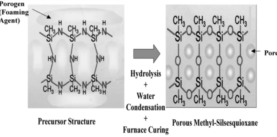
Fig. 2. Method of precursor structure transfer to final porous-polysilazane(PPSZ) structure. (100) orientation. Before film deposition, they were
boiled in H SO qH O solution and heated to 120 8C2 4 2 2
for 20 min to remove particles on the surfaces. These
wafers were spin-coated with ultra low-k
Porous-Poly-silazane (PPSZ) solution at a spin speed of 2000 rev.y
min for 30 s on a model 100CBspin coater. Then, it was followed by baking steps, sequentially on hot-plates at 150 and 280 8C for 3 min. The coated wafers were then followed by a hydration treatment. They were left in cleanroom for 48 h. For the polymer-structure to be transformed to porous methyl-silsesquioxane through hydrolysis and condensation process as shown in the following w16,17x:
Hydrolysis:
'Si-NH-Si'qH O™'Si-NH 'qHOySi'2 2
'Si-NH qH O™'Si-OHqNH2 2 3
Condensation:
'Si-OHqHO-Si'™'SiyOySi'qH O2
Afterward, the resulted wafers were cured in a quartz
furnace at 400 8C for 30 min under N ambient. The2
final PPSZ films (called as-cured PPSZ) were formed
with a thickness of 400 nm(the final structure is shown
in Fig. 2). The thickness of the deposited PPSZ films
was measured at n and k 1200 analyzer, manufactured by the n and k company, by comparing the theoretical reflectance with the actual measurement of broad-band reflectance. After film formation, the CMP process was applied to the as-cured PPSZ films. The CMP
experi-ment was carried out on an IPECyWestech 372M CMP
processor with a Rodel IC 1400 pad on the primary polishing plated and Rodel Politex Regular embossed pad on the final buffering plated. A Rodel R200-T3 carrier film was used to provide buffer between the
526 T.C. Chang et al. / Thin Solid Films 447 – 448 (2004) 524–530 Table 1
Polished parameters of ultra low-k PPSZ in IPECyWeatech 372M CMP polisher
Polisher: 1st step(only)
IPEC372M
Phase 1 Phase 2
PlatenyCarrier speed 50y60 rev.ymin 30y40 rev.ymin
Down force 3.0 psi 1.5 psi
Back pressure 2.0 psi 0
Slurry flow rate 150 mlycm Rinse
Polishing pad Rodel politex regular E.娃
Carrier film Rodel R200-T3娃
Slurry formation Cu slurry TaN slurry
2 vol.% HNO ,3 10 wt.% colloidal silica,
5=10y2M citric acid, 10 vol.% H O ,
2 2
3 wt.% Al O2 3(0.1 mm) pH 8.5
carrier and wafer. The wafer was mounted on a template assembly for a single 6 in. wafer during the polishing experiment. In this experiment, two types of slurries were implemented separately to investigate the influence
on the characteristics of ultra low-k PPSZ films. One
was the slurry typically used in polishing Cu metal, provided from National Nano Device Laboratory. This
slurry consists of 2 vol.% HNO , 5=10y2 citric acid,
3
and 3 wt.% Al O2 3 (0.1 mm), which was marked as Cu
slurry. The pH value of Cu-slurry is 0.56. Besides, we investigated another type of colloidal silicate slurry
(marked as TaN slurry), which included 10 wt.%
col-loidal silica and 10 vol.% H O in DI water liquid. Its2 2
pH value is 8.5. In addition, the polishing parameters, such as pad, down force, back pressure, platen and carrier rotation speeds, and slurry flow rate are shown on Table 1 for these two slurries. The structure properties of the PPSZ films were studied using Fourier transform
infrared spectroscopy(FTIR). The surface morphologies
of the polished films were investigated by atomic force
microscopy(AFM). Electrical characteristics of polished
PPSZ films were performed on the
metal-insulator-semiconductor (MIS) capacitor with metallic copper
deposition as the top electrode and aluminum deposition
as backside electrode. Leakage current–voltage (IyV)
and capacitance–voltage (CyV) characteristics were
also used to analyze the leakage current behaviors and to measure the dielectric constants of polished PPSZ films, respectively. During the operation of IC, it works at higher temperature and bias than its off state. In this situation, the copper may drift into the dielectric much
easily. Therefore, high bias and temperature stress(BTS)
was performed to evaluate the reliability under IC operation condition. In this work, BTS was performed
by applying an electric field at 2 MVycm on the MIS
capacitor at 150 8C for 1000 s. Before BTS testing, the leakage current of polished PPSZ films was measured at room temperature at 150 8C. After BTS testing, the
leakage current was measured again at 150 8C and room temperature sequentially.
3. Results and discussions
In order to obtain global planarization of multilevel interconnection and desirable pattern, the detection of end point of metal CMP must be concerned in the Cu damascene process. However, it is found that the
remov-al rate of ultra low-k PPSZ film with TaN slurry is 17
nmymin, which is lower (68.1 nmymin) than that of
polishing TaN with the same slurry. On the other hand,
the removal rate of ultra low-k PPSZ with Cu slurry is
only 3 nmymin, which is much lower than that of
polishing Cu with the same slurry. The results indicate that the difference in removal rate of copper or tantalum with respect to PPSZ is high and can distinguish the detection of end point much easily. In addition, the dielectric integrity and surface topography of ultra
low-k PPSZ films after metal CMP process has to be
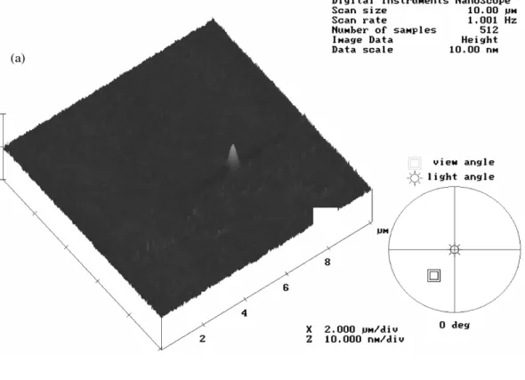
remained at acceptable region to meet requires of mul-tilevel interconnection. AFM images of PPSZ surface after CMP process with TaN and Cu slurries are shown in Fig. 3a and b, respectively. It indicates that there are smooth PPSZ surface after CMP polishing no matter
with TaN or Cu slurries, the roughness (Ra) of PPSZ
films is approximately 0.189 and 0.253 nm after TaN and Cu slurries polishing, respectively. This result indi-cates that the removal rate of copper and tantalum with
respect to low-k PPSZ film is high and can obtain
planarization surface after TaN or Cu CMP process. The FTIR spectra of post-CMP PPSZ with TaN or Cu slurries are given in Fig. 4. It is revealed that the Si–C and C–H bonds intensity of polished PPSZ films are still remand-ed at high level after metal CMP process. This provides evidence that the chemical structure of PPSZ film would not damage after CMP procedure with these polished slurries. Fig. 5a and b show the leakage current and
528 T.C. Chang et al. / Thin Solid Films 447 – 448 (2004) 524–530
Fig. 4. FTIR spectra of PPSZ films polished with TaN or Cu slurries
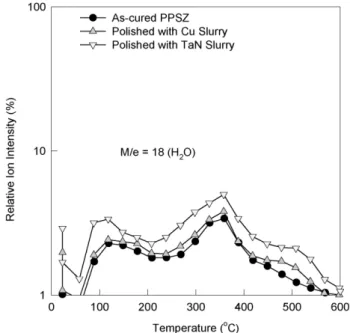
Fig. 6. The TDS moisture desorption spectra of PPSZ polished with TaN or Cu slurries.
Fig. 5. Dielectric properties of PPSZ films polished with TaN or Cu slurries:(a) Leakage current density of post-CMP PPSZ films as a function
of electric field;(b) dielectric constants of post-CMP PPSZ films.
dielectric constant of PPSZ after the CMP process with TaN or Cu slurries. The leakage current of post-CMP PPSZ is similar to as-cured PPSZ film regardless of PPSZ films polished with TaN or Cu slurries. The dielectric constants of post-CMP PPSZ films slightly increases from 2.25 of as-cured PPSZ film to the region of 2.3 to 2.4 as well, as shown in Fig. 5b. However, it still accords with the requirement of low-k materials. It
appears that the electrical properties of PPSZ cannot be
degraded during CMP process with TaN or Cu slurries. Fig. 6 reveals the tendency of moisture desorption during the raised temperature period in temperature desorption system. The concentrations of moisture desorption of PPSZ, polished with TaN or Cu slurries are silimar to that of as-cured PPSZ films. This is believed that the film characteristics are not changed after CMP process. This result is consistent with the electrical properties of PPSZ films polished by metal polishing slurries.
More-Fig. 7. Leakage current density of Cu-electrode polished PPSZ film after 2 Mvycm at 150 8C for 1000 sec BTS stress measured at room temperature
at 150 8C(a) with TaN slurry (b) with Cu slurry.
over, in order to investigate the reliability of polished PPSZ with copper, the higher temperature measurement and BTS tests were conducted to evaluate the reliability of post-CMP PPSZ. Fig. 7a and b show the leakage current density of these post-CMP PPSZ films before and after BTS test at high and low temperature. The leakage current densities of the post-CMP PPSZ with
TaN or Cu slurries donot arise at all after BTS stress
(versus pre-BTS stressing post-CMP PPSZ films). With
either TaN or Cu slurry, the leakage current of post stressed PPSZ is really close to that of pre-stressing ones and even electrical measurements were implement-ed at high temperature. This implies that the electrical reliability of PPSZ can be maintained even after metal
530 T.C. Chang et al. / Thin Solid Films 447 – 448 (2004) 524–530
CMP process. As a result, the low-k PPSZ films after
the CMP processes with Cu or Ta slurries will have good resistance to copper drift at high field and temper-ature operation conditions. These foregoing results sug-gest that the ultra low-k PPSZ film has a lot of potential
for application in next generation of IC manufacture. 4. Conclusion
The CMP of organic ultra low-k(k;2.2) PPSZ films
with Ta and Cu slurries provided from national nano-device laboratory do not damage dielectric properties of
PPSZ. The ultra low-k PPSZ materials have low polish
rate as regard to the polish of Ta or Cu metal during damasence manufacture, and thus benefits the detection of end point of metal polish much easily. Moreover, the electrical properties of post-CMP PPSZ films can remain in low-k characteristics. Even after the high temperature
and bias stress condition, the leakage currents do not arise and degrade at all. According to our results a reliable CMP process of damascene manufacture can be obtained by using our proposed TaN or Cu slurry. It is believed that the integration between PPSZ and Cu has promising potential in the next generation of ICs. Acknowledgments
This work was performed at National NanoDevice Laboratory and was supported by the Clariant Corpora-tion in Tokyo, Japan, and the NaCorpora-tional Science Council of the Republic of China under Contract, Nos. NSC92-2112-M-110-020 and NSC92-2215-E-110-006.
References
w1x M. Morgen, E.T. Ryan, J.H. Zhao, Annu. Rev. Mater. Sci. 30 (2000) 645.
w2x R.H. Havemann, J.A. Hutchby, Proc. IEEE 89(5) (May 2001)
586–601, Sp. Iss. SI.
w3x A. Jain, S. Rogojevic, S. Ponoth, Thin Solid Films 398(2001)
513.
w4x S. Lakshminarayanan, P. Wright, J. Pallinti, IEEE Int. Intconn.
Technol. Conf. 2002, pp. 99–101.
w5x J. Chen, S. Parikh, T. Vo, S. Rengarajan, T. Mandrekar, P.
Ding, L. Chen, R. Mosely, IEEE Int. Intconn. Technol. Conf. 2002, pp. 185–187.
w6x P. Wrschka, J. Hernandez, G.S. Oehrlein, J. King, J.
Electro-chem. Soc. 147(2000) 706.
w7x A.K. Sikder, A. Kumar, J. Electron. Mater. 31(2002) 1016. w8x A.L.S. Loke, J.T. Wetzel, C. Ryu, W.J. Lee, S.S. Wong, VLSI
Technology, 1998. Digest of Technical Papers in 1998 Sym-posium, 1998, pp. 26.
w9x P.T. Liu, T.C. Chang, Y.L. Yang, Y.F. Cheng, F.Y. Shih, J.K.
Lee, E. Tsai, S.M. Sze, Jpn. J. Appl. Phys. 38(1999) 6247. w10x B. Trednnick, J. Lee, K. Holland, T. Bibby, No.
96-ISMIC-100P, in: Proceedings of the First International Chemical Mechanical Polish(CMP) for VLSIyULSI Multilevel
Intercon-nection Conference, CMP-MIC, 1996, pp. 107.
w11x The National Technology Roadmap for Semiconductors, 1997,
p. 99.
w12x C.S. Xu, E. Zhao, R. Jairath, Electrochem. Solid State Lett. 1 (1998) 181.
w13x M.E. Gross, C Lingk, W.L. Brown, Solid State Technol. 42 (1999) 47.
w14x P.T. Liu, T.C Chang, M.C Huang, M.S. Tsai, S.M. Sze, J. Vac.
Sci. Technol. B19(2001) 1212.
w15x C.L. Borst, D.G. Thakurta, W.N. Gill, J. Electron. Packag. 124 (2002) 362.
w16x A.M. Padovani, L. Rhodes, S.A.B. Allen, P.A. Kohl, J.
Elec-trochem. Soc. 149(2002) F161.
w17x T. Aoki, Y. Shimizu, T. Kikkawa, Low-dielectric Constant
Materials V, 565, Materials Research SocietyWarrendale, Penn-sylvania: Materials Research Society, 1999, p. 41.