IEEE ELECTRON DEVICE LETTERS, VOL. 29, NO. 2, FEBRUARY 2008 171
Characteristics of PBTI and Hot Carrier Stress
for LTPS-TFT With High-
κ
Gate Dielectric
Ming-Wen Ma, Student Member, IEEE, Chih-Yang Chen, Student Member, IEEE, Chun-Jung
Su, Student Member, IEEE, Woei-Cherng Wu, Student Member, IEEE, Yi-Hong Wu, Kuo-Hsing Kao,
Tien-Sheng Chao, Senior Member, IEEE, and Tan-Fu Lei, Member, IEEE
Abstract—In this letter, the characteristics of positive bias
tem-perature instability (PBTI) and hot carrier stress (HCS) for the low-temperature poly-Si thin-film transistors (LTPS-TFTs) with HfO2 gate dielectric are well investigated for the first time. Under room temperature stress condition, the PBTI shows a more serious degra-dation than does HCS, indicating that the gate bias stress would dominate the hot carrier degradation behavior for HfO2 LTPS-TFT. In addition, an abnormal behavior of the Imin degradation with different drain bias stress under high-temperature stress con-dition is also observed and identified in this letter. The degradation of device’s performance under high-temperature stress condition can be attributed to the damages of both the HfO2 gate dielectric and the poly-Si grain boundaries.
Index Terms—High-κ, hot carrier stress (HCS), low-temperature poly-Si thin-film transistors (LTPS-TFTs), positive bias temperature instability (PBTI).
I. INTRODUCTION
L
OW-TEMPERATURE poly-Si thin-film transistors (LTPS-TFTs) have been used for active-matrix liquid crystal displays on glass substrate as pixel and driving integrated cir-cuits instead of amorphous silicon [1]–[6]. Therefore, high-performance TFTs with high driving current, low threshold voltage (VT H), and subthreshold swing (S.S.) are requiredur-gently for high-speed display driving circuits. In order to achieve high-performance LTPS-TFT, employing high-κ gate dielec-tric is one of the effective ways to improve the performance of LTPS-TFT [7]–[9]. In addition, quality deposited low-temperature SiO2 [like plasma-enhanced chemical vapor
depo-sition (PECVD), SiO2] is generally employed as the gate
dielec-tric of the conventional LTPS-TFT. Comparing with low-quality deposited low-temperature SiO2, low-temperature deposited
high-κ gate dielectric could have better quality and be more suitable for the replacement of the conventional low-temperature SiO2. However, the reliability issue of LTPS-TFT with high-κ
Manuscript received October 4, 2007; revised November 14, 2007. This work was supported by the National Science Council, Taiwan, under Contract NSC-95-2221-E-009-272. The review of this letter was arranged by Editor J. Sin.
M.-W. Ma, C.-Y. Chen, C.-J. Su, and T.-F. Lei are with the In-stitute of Electronics, National Chiao Tung University, Hsinchu, Taiwan 300, R.O.C. (e-mail: [email protected]; [email protected]; [email protected]; [email protected]).
W.-C. Wu, K.-H. Kao, and T.-S. Chao are with the Institute and Depart-ment of Electrophysics, National Chiao Tung University, Hsinchu, Taiwan 300, R.O.C. (e-mail: [email protected]; [email protected]; [email protected]).
Y.-H. Wu is with the Department of Electronic Engineering, Feng Chia Uni-versity, Taichung 40724, Taiwan, R.O.C. (e-mail: [email protected]). Color versions of one or more of the figures in this letter are available online at http://ieeexplore.ieee.org.
Digital Object Identifier 10.1109/LED.2007.914091
gate dielectric is still not deeply studied. In this letter, positive bias temperature instability (PBTI) and hot carrier stress (HCS) of HfO2 LTPS-TFT are well investigated for the first time.
II. EXPERIMENTALPROCEDURE
The fabrication of devices started by depositing a 50-nm-undoped amorphous Si (α-Si) layer at 550◦C in a low-pressure chemical vapor deposition system on Si wafers capped with a 500 nm thermal oxide layer. Then, the 50 nm α-Si layer was recrystallized by solid-phase crystallization process at 600◦C for 24 h in a N2 ambient. Then, a 500 nm PECVD oxide was
deposited at 300◦C for device isolation. The device active re-gion was formed by patterning and etching the isolation oxide. The source and drain regions in the active device region were implanted with phosphorus (15 keV at 5× 1015cm−2) and ac-tivated at 600◦C for 24 h annealing in a N2 ambient. A 75 nm
HfO2 with effective oxide thickness 14.7 nm was deposited
by electron-beam evaporation system. After the patterning of source/drain contact holes, aluminum was deposited by thermal evaporation system as the gate electrode and source/drain con-tact pad. Finally, the TFT devices were completed by the concon-tact pad definition.
Devices with gate length (L) and width (W) of 10 and 100 µm were measured. The VT H is defined as the gate voltage at which
the drain current reaches 100 nA× W /L and VD S = 0.1 V. The transfer characteristics ID–VG of HfO2 LTPS-TFT are
mea-sured at VD = 0.1 V and VG =−0.5 to 4 V. The nominal
op-erating voltage of this LTPS-TFT with HfO2 gate dielectric is
set to be 4 V due to its excellent S.S. and low threshold voltage
(∼0.9 V). The PBTI stress was set at VG − VT H = 5 V and
VD = VS = 0 V. Two HCS modes are also investigated, namely
HCS-A: VG − VT H = VD = 5 V, VS = 0 V, and HCS-B: VG− VT H = 5 V, VD = 10 V, VS = 0 V. All measurements were
performed at temperature T = 25◦C and 125◦C, respectively. III. RESULTS ANDDISCUSSION
Fig. 1 shows the transfer characteristics of HfO2 LTPS-TFT
before and after 1000 s of PBTI and HCS-B stresses at 25◦C, re-spectively. We can observe that the shift of VT H, and degradation
of S.S. and Gm of device under the PBTI are all more serious
than those of devices under HCS-B. The extracted parameters of these HfO2LTPS-TFTs are listed in Table I. It reveals that the
gate bias stress would be the dominant factor of degradation for the HfO2 LTPS-TFT under HCS. The difference between HCS
and PBTI is the vertical electric field near the drain side. This
172 IEEE ELECTRON DEVICE LETTERS, VOL. 29, NO. 2, FEBRUARY 2008
Fig. 1. Transfer characteristics (ID–VG and Gm) of the HfO2 LTPS-TFT
before and after 1000 s of PBTI and HCS-B stresses at 25◦C. TABLE I
IMPORTANTPARAMETERS OF THEHfO2LTPS-TFT BEFORE ANDAFTER1000 s
OFPBTIANDHCS-B STRESSES AT25◦C
indicates that the stress of vertical electric field plays a more important role than does the stress of lateral electrical field for HfO2LTPS-TFT. Fig. 2 shows the gate leakage current of HfO2
LTPS-TFT before and after 1000 s of PBTI and HCS-B stresses at 25◦C and 125◦C, respectively. A larger gate leakage cur-rent reduction of the PBTI device indicates that more electrons were trapped in HfO2 under PBTI stress than under HCS-B
stress. It shows that applying a drain voltage would decrease the behavior of electrons trapping in HfO2, indicating that the
vertical electrical field could introduce more trapped electrons in HfO2 than the impact ionization of HCS does. Similar
be-havior of carrier trapping in HfO2gate dielectric during HCS is
also observed for complementary metal–oxide–semiconductor Si nanoelectronics [10].
In addition to the degradation of VT H, Gm, and S.S., the Im in(from Fig. 1) is almost invariant after 1000 s of PBTI and
HCS-B stresses, indicating that the poly-Si grain boundaries of channel film are not significantly damaged [11]. This shows that the main degradation of HfO2 LTPS-TFT at 25◦C under PBTI
and HCS-B stresses is due to the damage and electron trapping of HfO2gate dielectric.
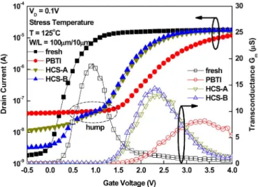
Fig. 3 shows the transfer characteristics of HfO2 LTPS-TFT
before and after 1000 s stress at 125◦C under PBTI, HCS-A, and HCS-B stresses, respectively. The trend of VT H shift, Gm
degradation, and S.S. degradation is the same as measured at 25◦C. However, the behavior of Im inat 125◦C is different from
the Im inat 25◦C. The PBTI device shows the most serious Im in
degradation (from 2× 10⁻⁹to 4× 10⁻⁸A), and the HCS-A de-vice shows a little improvement (from 4× 10⁻⁸to 1× 10⁻⁸A) of Im in as compared to the PBTI device. The HCS-B device
Fig. 2. Gate leakage current of the HfO2LTPS-TFT before and after 1000 s
of PBTI and HCS-B stresses at 25◦C and 125◦C.
Fig. 3. Transfer characteristics of the HfO2 LTPS-TFT before and after
1000 s of PBTI, HCS-A, and HCS-B stresses at 125◦C.
shows the smallest degradation of Im in among these samples
(from 2× 10⁻⁹ to 3.3× 10⁻⁹ A). The Im in can be attributed
to two sources: one is coming from the gate leakage current and the other is coming from the junction leakage current of drain side [11]. In this case, the gate leakage (from Fig. 2) has been shown to be too low to contribute the Im in of
de-vices. Therefore, we can conclude that the Im in degradation is
coming from the junction leakage current of drain side. How-ever, an increased junction leakage current would be attributed to the degradation of poly-Si and HfO2/poly-Si interface. We
can observe from Fig. 1 that the degradation of HfO2/poly-Si
interface would contribute to a negligible increase of junction leakage current. Therefore, we could conclude that the increased junction leakage would be attributed to the damage of poly-Si grain boundaries. In PBTI device, the highest Im inindicates the
most serious grain boundaries damage, resulting in significant increase of Im in. In HCS-A case, drain bias would make the
ver-tical electric field near the drain side lower and improve the Im in
MA et al.: CHARACTERISTICS OF PBTI AND HOT CARRIER STRESS 173
case, the vertical electric field would be decreased further. Dur-ing positive gate bias stress, electrons would be accelerated by positive gate voltage and move toward the HfO2/poly-Si
inter-face. The accelerated electrons would collide with the weak bond of the grain boundaries to damage the poly-Si channel film and the HfO2/poly-Si interface to generate the trap states
to increase the drain leakage current Im in, S.S., and reduce the
transconductance Gm. Compared with stresses at 25◦C, stresses
at 125◦C would result in more serious degradation and a hump behavior of transfer characteristics of HfO2 LTPS-TFT due to
higher carrier energy and lattice collision probability. Apply-ing a drain bias would decrease the vertical field near the drain side and result in less junction damage and fewer electron trap-ping. The large drain bias would make the device have less Im in
degradation and also a varying threshold voltage along the chan-nel due to different degrees of grain boundaries damages and electron trapping, respectively. The local threshold voltage and grain boundaries damage near the drain side would be smaller than the one near the source side. Therefore, a hump in trans-fer characteristic of the device is observed in HCS-A case, as shown in Fig. 3, and the hump becomes significant in the HCS-B case. Based on the above mentioned results, stresses at 125◦C show that the degradation of HfO2 LTPS-TFT is attributed to
the damages of both HfO2and poly-Si grain boundaries.
IV. CONCLUSION
The PBTI and HCS of HfO2 LTPS-TFT have been well
in-vestigated for the first time. We conclude that the vertical elec-tric field stress dominated the hot carrier degradation behav-iors for HfO2 LTPS-TFT devices. In addition, a hump behavior
of the transfer characteristic of HfO2 LTPS-TFT under
high-temperature stress condition was also observed and identified in this letter. The results show that applying a drain bias under stress would obviously impact the reliability of LTPS-TFT with high-κ gate dielectric.
ACKNOWLEDGMENT
The authors would like to thank the processes support from the National Nano Device Laboratories and the Nano Facility Center of the National Chiao Tung University.
REFERENCES
[1] G. K. Guist and T. W. Sigmon, “High-performance thin-film transistors fabricated using excimer laser processing and grain engineering,” IEEE Trans. Electron Devices, vol. 45, no. 4, pp. 925–932, Apr. 1998. [2] Y. W. Choi, J. N. Lee, T. W. Jang, and B. T. Ahn, “Thin-film transistors
fabricated with poly-silicon films crystallized at low temperature by mi-crowave annealing,” IEEE Electron Device Lett., vol. 20, no. 1, pp. 2–4, Jan. 1999.
[3] C. W. Lin, M. Z. Yang, C. C. Yeh, L. J. Cheng, T. Y. Huang, H. C. Cheng, H. C. Lin, T. S. Chao, and C. Y. Chang, “Effects of plasma treatments, substrate types, and crystallization methods on performance and reliability of low temperature polysilicon TFTs,” in IEDM Tech. Dig., 1999, pp. 305– 308.
[4] K. M. Chang, W. C. Yang, and C. P. Tsai, “Electrical characteristics of low temperature polysilicon TFT with a novel TEOS/oxynitride stack gate dielectric,” IEEE Electron Device Lett., vol. 24, no. 8, pp. 512–514, Aug. 2003.
[5] J.-H. Jeon, M.-C. Lee, K.-C. Park, S.-H. Jung, and M.-K. Han, “A new poly-Si TFT with selectively doped channel fabricated by novel excimer laser annealing,” in IEDM Tech. Dig., 2000, pp. 213–216.
[6] W. G. Hawkins, “Polycrystalline-silicon device technology for large-area electronics,” IEEE Trans. Electron Devices, vol. 33, no. 4, pp. 477–481, Apr. 1986.
[7] B. F. Hung, K. C. Chiang, C. C. Huang, A. Chin, and S. P. McAlister, “High-performance poly-silicon TFTs incorporating LaAlO3 as the gate
dielectric,” IEEE Electron Device Lett., vol. 26, no. 6, pp. 384–386, Jun. 2005.
[8] Z. Jin, H. S. Kwok, and M. Wong, “High-performance polycrystalline SiGe thin-film transistors using Al2O3 gate insulators,” IEEE Electron
Device Lett., vol. 19, no. 12, pp. 502–504, Dec. 1998.
[9] C.-P. Lin, B.-Y. Tsui, M.-J. Yang, R.-H. Huang, and C. H. Chien, “High-performance poly-silicon TFTs using HfO2gate dielectric,” IEEE
Elec-tron Device Lett., vol. 27, no. 5, pp. 360–363, May 2006.
[10] H. Park, R. Choi, S. C. Song, M. Chang, C. D. Young, G. Bersuker, B. H. Lee, J. C. Lee, and H. Hwang, “Decoupling of cold carrier effects in hot carrier reliability of HfO2gated nMOSFETs,” in Proc. Int. Rel. Phys.
Symp., 2006, pp. 200–203.
[11] K. R. Olasupo and M. K. Hatalis, “Leakage current mechanism in sub-micron polysilicon thin-film transistors,” IEEE Trans. Electron Devices, vol. 43, no. 8, pp. 1218–1223, Aug. 1996.