driving capability to trigger the ESD clamp device on. These ESD protection designs have been successfully verified in two different 0.13-μm 1.2-V CMOS processes to provide excellent on-chip ESD protection for 1.2-V/3.3-V mixed-voltage I/O buffers.
Index Terms—Electrostatic discharge (ESD), low-voltage CMOS, mixed-voltage I/O, substrate-triggered technique.
I. INTRODUCTION
W
ITH the decrease of the power supply voltage for low-power applications, the thickness of gate oxide in advanced CMOS technologies has been scaled down to improve circuit performance and to meet the gate-oxide reliability. For whole system integration, the I/O buffers may drive or receive high-voltage signals to communicate with other ICs in the microelectronic system. However, the traditional I/O buffers will suffer from gate-oxide reliability and leakage current path when the I/O buffers receive high-voltage signals. Therefore, the I/O buffers should be designed with consideration on high-voltage tolerance to prevent overstress high-voltage on the thinner gate oxide of the devices in I/O buffers [1]–[3]. To avoid gate-oxide reliability issue without using additional thick gate gate-oxide process, the stacked NMOS configuration has been widely used in the mixed-voltage I/O buffers. However, the stacked NMOS configuration usually has a lower electrostatic discharge (ESD) level and slow turn-on speed of the parasitic lateral n-p-n device, as compared with the single NMOS [4], [5]. The disadvantages result from the longer base width of the lateral n-p-n BJT in the stacked NMOS devices. Therefore, additional ESD protection design must be provided to protect the stacked NMOS in the mixed-voltage I/O buffer without additional leakage current path [6].Manuscript received August 27, 2007; revised January 17, 2008 and May 15, 2008. Current version published March 6, 2009. This work was supported in part by the National Science Council (NSC), Taiwan, under Contract NSC 97-2221-E-009-170 and in part by United Microelectronics Corporation, Taiwan.
M.-D. Ker is with the Institute of Electronics, National Chiao-Tung Univer-sity, Hsinchu 300, Taiwan, and also with the Department of Electronic Engi-neering, I-Shou University, Kaohsiung 84001, Taiwan (e-mail: mdker@ ieee.org).
C.-T. Wang is with the Institute of Electronics, National Chiao-Tung Univer-sity, Hsinchu 300, Taiwan (e-mail: [email protected]).
Digital Object Identifier 10.1109/TDMR.2008.2008639
To achieve a good whole-chip ESD protection scheme for the mixed-voltage I/O applications, it is required to design the low leakage power-rail ESD clamp circuit with only low-voltage devices that can sustain the high power-supply voltage without suffering gate-oxide reliability [8]–[11]. Recently, the ESD protection scheme for the 3.3-V mixed-voltage I/O buffers with 1-V/2.5-V dual gate low-voltage devices has been successfully verified in 0.13-μm CMOS process [10]. However, this prior design still needs extra mask-set to implement the thick gate-oxide devices (2.5-V devices). Therefore, how to design an effective ESD protection circuit with only low-voltage devices without suffering gate-oxide reliability for mixed-voltage I/O buffer with 3× VDD input tolerance is a significant challenge. In this paper, two new high-voltage-tolerant ESD protection designs realized with only 1 × VDD low-voltage devices to protect the mixed-voltage I/O buffer with 3 × VDD input tolerance are proposed [12], [13]. These new ESD protection designs have different efficient ESD detection circuit to trigger on the ESD clamp device, so that the turn-on efficiency of ESD clamp device can be significantly improved. The proposed ESD protection design has been successfully verified in two different 0.13-μm 1.2-V CMOS processes.
II. ESD PROTECTIONSCHEME FOR3× VDD-TOLERANT
MIXED-VOLTAGEI/O BUFFER
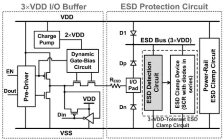
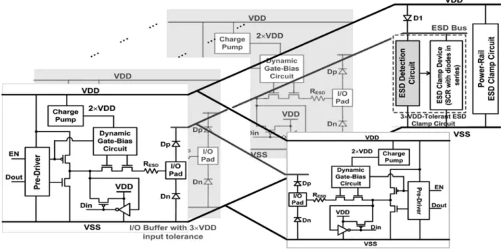
To improve ESD robustness of the mixed-voltage I/O inter-faces, an ESD protection concept by using the on-chip ESD bus had been reported [14]. However, in this prior art, the gate-oxide reliability was not considered in its circuit imple-mentation. With consideration on the gate-oxide reliability, the new ESD protection scheme for mixed-voltage I/O buffer with 3 × VDD input tolerance is shown in Fig. 1. The circuit design for 3× VDD-tolerant I/O buffer realized with only 1 × VDD devices has been reported in [7]. In the 3 × VDD I/O buffer, the dynamic gate-bias circuit controls the gate voltages of the stacked NMOS, as shown in Fig. 1. When the I/O buffer receives a logic high (3× VDD), the gate voltages of the stacked NMOS are biased at VDD and 2 × VDD from left to right, respectively. When operating at other receiving or transmitting modes, the stacked NMOS can also be well biased by the dynamic gate-bias circuit. Therefore, the 3 × VDD I/O buffer can tolerate 3 × VDD input signals without
Fig. 1. Proposed ESD protection scheme for mixed-voltage I/O buffer with 3× VDD input tolerance realized with only 1 × VDD devices.
gate-oxide reliability issue. The detailed circuit implantation to realize such dynamic gate-bias circuit, which can trace the voltage level at the I/O pad, can be found in [7].
To receive the input signals with 3.3-V voltage level, the traditional ESD protection with direct diode connection from I/O pad to VDD of 1.2 V is forbidden. Therefore, the ESD protection circuit is realized with diodes Dp, Dn, D1, ESD bus, ESD detection circuit, ESD clamp device, and the power-rail ESD clamp circuit between VDD and VSS, as shown in Fig. 1. Under positive-to-VSS (PS-mode) ESD stress on I/O pad, the ESD current can be discharged through the diode Dp to the ESD bus and then through the ESD clamp device [silicon control rectifier (SCR)] to the grounded VSS, instead of through stacked NMOS in the I/O buffer to ground. Under positive-to-VDD (PD-mode) ESD stress on I/O pad, the ESD current can be discharged through Dp, ESD bus, and the ESD clamp device to VSS power line, and then through the power-rail ESD clamp circuit between VDD and VSS to the grounded VDD. Under negative-to-VSS (NS-mode) ESD stress on I/O pad, the negative ESD current can be discharged through the diode Dn in forward-biased condition to the grounded VSS. Under negative-to-VDD (ND-mode) ESD stress on I/O pad, the negative ESD current can be discharged through Dn to the floating VSS power line, and then through the power-rail ESD clamp circuit between VDD and VSS to the grounded VDD. The four modes of ESD stresses on the mixed-voltage I/O pad to VDD or VSS have the corresponding well-designed ESD discharging paths in the proposed ESD protection scheme.
When an ESD stress is applied to the I/O pad, the transient voltage-limiting criteria of the 3× VDD tolerant I/O buffer can be expressed as
Vmax= IESD× RESD+ VBD_NMOS (1)
where Vmax is the maximum transient voltage that the 3 ×
VDD I/O buffer can sustain, IESDis the ESD current, and the
VBD_NMOS is the transient breakdown voltage of the stacked
NMOS between the RESDand VSS in Fig. 1. Under the ESD
stress event, all nodes in the 3× VDD I/O buffer are floating
initially. The transient breakdown voltage VBD_NMOS is given
by the drain breakdown voltage of the stacked NMOS in the 3× VDD I/O buffer. In order to prevent the ESD current from injecting into the 3× VDD I/O buffer, the trigger voltage and the clamp voltage of the 3× VDD-tolerant ESD clamp circuit should be less than Vmax. The clamp voltage of the 3×
VDD-tolerant ESD clamp circuit can be expressed as
Vclamp= VD+ Vhold+ IESD× Ron (2)
where VD is the voltage drop across the diode Dp, Vhold is
the holding voltage of the 3 × VDD-tolerant ESD clamp circuit, and Ronis the equivalent turn-on resistance of the diode
Dp, parasitic routing resistance, and the 3 × VDD-tolerant ESD clamp circuit. Therefore, RESD should be designed to
be slightly greater than some critical value to make sure that
Vclampis less than Vmax. The criterion of RESDcan be found as
RESD> Ron+
VD+ Vhold− VBD_NMOS
IESD
. (3) In this paper, VBD_NMOS of∼7.5 V is measured from the
breakdown voltage of the stacked NMOS. For a VD of 0.7 V,
Vhold of 3.3 V, and Ron of 3 Ω, the resistance RESD should
be greater than 0.4 and 1.7 Ω for 2 kV (IESD of 1.33 A) and
4 kV (IESDof 2.66 A) human-body-model (HBM) ESD levels,
respectively. Under these criteria, the ESD current is discharged through the proposed ESD protection circuit rather than the 3× VDD I/O buffer under ESD stress, so that the stacked NMOS in the 3× VDD I/O buffer can be safely protected by the proposed ESD protection scheme in Fig. 1.
The power-rail ESD clamp circuit between VDD and VSS can be realized by the traditional RC-based ESD detection circuit [15]. The SCR device, which is composed of the cross-coupled n-p-n and p-n-p BJTs with regenerative feedback, with a low holding voltage can sustain a high ESD level within a small silicon area in CMOS technology [16]. However, the main concerns of SCR device as the ESD clamp device are the slow turn-on speed, high switching voltage, and latchup issue. To solve the latchup issue, several diodes are added in
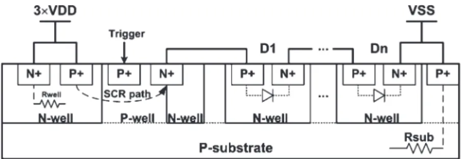
Because these two ESD protection design were implemented in two different foundries, the electrical characteristic of SCR devices used as ESD clamp device were quite different. The holding voltage of SCR device is dominated by the doping pro-files correlated with the process of each foundry, and therefore the numbers of diodes added in series with SCR for two ESD clamp circuit are different to avoid the latchup issue. In this paper, three (two) diodes are added with SCR in series to in-crease its overall holding voltage to approximately 4 V for such 3.3-V tolerant ESD clamp circuit A (B). The holding voltage a little higher than 3.3 V is used to overcome overshooting supply voltage. The device structure of the ESD clamp device used in these work is shown in Fig. 2. The purpose of the additional N-well region under the N+ diffusion at the cathode of the SCR device with the substrate-triggered technique is to further enhance the on speed of the SCR device for better turn-on efficiency, because that can increase the equivalent substrate resistance (Rsub) in this device structure.
To avoid the ESD damage on I/O buffer before ESD clamp device is turned on, the substrate-triggered technique is used to quickly trigger on the ESD clamp device. Because ESD bus line will be biased at 3.3 V through the diode Dp when 3.3-V input signals reach to the I/O pad, the ESD detection circuit connected between ESD bus and VSS must sustain the high-voltage (3.3 V) stress during normal circuit operating condition. Some ESD detection circuits proposed to increase the turn-on speed of SCR device will suffer gate-oxide reliability issue under 3.3-V bias with only 1.2-V low-voltage devices [18]. Therefore, how to design a turn-on-efficient ESD detection circuit with only 1.2-V devices to sustain 3.3-V bias becomes a quite significant challenge to this 1.2/3.3-V mixed-voltage I/O buffer.
III. 3× VDD-TOLERANTESD CLAMPCIRCUITS
During normal circuit operating condition with 1.2-V VDD power supply and grounded VSS, when a 3 × VDD (3.3-V) input signal is applied to the I/O pad, the voltage level at the internal ESD bus will be charged up to 3.3 V through the diode Dp connected between I/O pad and ESD bus. For the convenience of easily describing the circuit operation of the 3× VDD-tolerant ESD clamp circuit with HSPICE simulations, the ESD bus is treated as an external 3.3 V power supply in this section.
Fig. 3. Circuit implementation of the 3× VDD-tolerant ESD clamp circuit A realized with 1× VDD devices.
A. 3× VDD-Tolerant ESD Clamp Circuit A
The ESD clamp circuit that can be operated under 3.3-V bias with only 1.2-V low-voltage devices is shown in Fig. 3. Under normal circuit operating condition, the diode-connected PMOS (Mp1∼ Mp3) are used as the voltage divider to bias the substrate driver (Mn1, Mp4, and Mp5) of the ESD detection circuit, where a deep N-well is used in Mn1 to avoid the gate-oxide overstress between gate and bulk. The NMOS (Mn2) is used to keep the voltage level of the trigger node at VSS, so the ESD clamp device is guaranteed to be kept off in the normal circuit operating condition. Here, the RC time constant of R1 and Mp7 should be designed around the order of ∼1 μs to distinguish the normal circuit operating condition from the ESD transition [11].
1) Operation Under Normal Circuit Operating Condition:
During normal circuit operating condition, the node 1 and node 2 in the ESD detection circuit will be biased at 2.2 and 1.1 V, respectively. The node 5 is biased at 1.2 V through the 1-kΩ resistor of R2 to VDD, so that Mp5 is turned off. There is no trigger current generated from the ESD detection circuit into the ESD clamp device. In addition, the Mn2 in the turned-on state, whose gate is connected to VDD through the resistor of R2, can increase the noise margin of the ESD detection circuit to guarantee the ESD clamp device against false triggering during the normal circuit operating conditions. All devices in
Fig. 4. Cross-sectional view of the NMOS Mn1 and the Hspice-simulated voltages at the nodes of ESD detection circuit under the normal circuit operating condition.
the proposed ESD detection circuit with 1.2-V gate oxide can be free from gate-oxide reliability issue under the ESD bus of 3.3 V.
In this ESD detection circuit, the drain-to-gate voltage of Mn1 is (3.3 V–2.2 V), where Mn1 is working at inversion region under the normal circuit operating conditions. However, the induced channel region of Mn1 could be insufficient to shade the strength of the electric field across the gate and bulk if its bulk region is grounded. There is somewhat gate-oxide reliability concern on Mn1 if its bulk is grounded. Therefore, to avoid this possible issue, the bulk of Mn1 is connected to its own source node. To avoid the leakage current path through the bulk (p-well) of Mn1 to the grounded p-substrate, the bulk (p-well) of Mn1 is isolated by the deep N-well with 3.3-V bias from the common p-substrate, as the diagram shown in Fig. 4. Fig. 4 also marks with the Spice-simulated voltages at the nodes of the ESD detection circuit during normal circuit operating condition. From these simulated voltages, the voltages between each two adjacent nodes of devices do not exceed their voltage limitation (1.32 V for 1.2-V devices). Therefore, the ESD detection circuit is free from the gate-oxide reliability issue.
2) Operation Under ESD Transition: When ESD voltage is
applied to the I/O pad with VSS relatively grounded, such ESD transient voltage will be conducted into ESD bus through the Dp diode in forward-biased condition. Therefore, the ESD bus will have a fast rising-up ESD voltage. The capacitor (Mp6) will couple some ESD transient voltage to the node 1 to turn on Mn1 and to pull up the node 3. The RC delay from R1 and Mp7 in the ESD detection circuit will keep the gate of Mp4 (node 4) at a relatively lower voltage level (compared to the node 3) for a long time. The VDD is initially floating with an initial voltage level of 0 V during a PS-mode ESD stress at I/O pad. Some ESD transient voltage would be coupled to VDD through the parasitic capacitance during ESD zapping, but the R2 and the parasitic capacitance at the gates of Mp5 and Mn2 will hold the gate of Mp5 at a low voltage level for a long time to keep Mp5 in on state. Therefore, Mp4 and Mp5, whose initial gate voltages are at low voltage level, can be quickly turned on by ESD energy to generate the substrate-triggered current
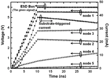
Fig. 5. Hspice-simulated voltages on the nodes of ESD detection circuit and the substrate-triggered current through Mp5 under 0-to-6 V ESD-like transition on ESD bus.
into the substrate of SCR. Then, the ESD clamp device can be quickly triggered on to discharge ESD current from ESD bus to VSS.
Fig. 5 shows the Hspice-simulated voltages and the substrate-triggered current of the ESD detection circuit under ESD tran-sition. A 0-to-6 V ESD-like voltage pulse with a rise time of 10 ns is applied to the ESD bus to simulate the ESD transient voltage. The Spice-simulated results show that the gate voltage of Mn1 (node 1) is quickly pulled high through Mp6, whereas the gate voltage of Mp4 (node 4) is kept low due to the RC time delay from R1 and Mp7. Therefore, the ESD clamp device can be triggered on to discharge ESD current from ESD bus to VSS. The substrate driver can provide the substrate-triggered current larger than 35 mA within 10 ns when the 0-to-6 V transient voltage is applied to ESD bus, as shown in Fig. 5. By selecting the suitable device dimensions of R1, Mp7, and the substrate driver (Mn1, Mp4, and Mp5), the peak current and the period of the substrate-triggered current can be adjusted to meet different applications or specifications.
B. 3× VDD-Tolerant ESD Clamp Circuit B
The other 3× VDD-tolerant power-rail ESD clamp circuit, which contains ESD clamp device and ESD detection circuit with additional control, is shown in Fig. 6, where the ESD clamp device is realized by a substrate-triggered SCR with two diodes in series. The new proposed 3× VDD-tolerant power-rail ESD clamp circuit is also realized with only 1.2-V low-voltage devices to operate at 3.3-V power supply (3× VDD) without the risk of gate-oxide reliability.
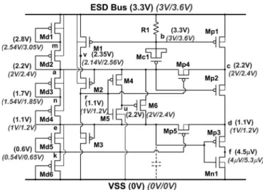
Under normal circuit operating condition, the diode-connected PMOS (Md1~Md6) are used as the voltage divider to bias the substrate driver (Mp1, Mp2, and Mp3) and the control circuit (M1∼ M6, Mp4 and Mp5) of the ESD detection circuit. Here, the RC time constant of R1 and Mc1 should be designed around the order of ∼1 μs to distinguish ESD stress event from the normal circuit operating conditions. Furthermore,
Fig. 6. Circuit implementation of the 3× VDD-tolerant ESD clamp circuit B realized with 1× VDD devices.
the special control circuit can further enhance the substrate-triggered current generated by substrate driver in ESD detection circuit.
1) Operation Under Normal Circuit Operating Condition:
During the normal circuit operating condition, the node a and node e in the ESD detection circuit are biased at 2.2 and 1.1 V, respectively. The gate voltage (node k) of Mp5 will be biased at 0.6 V due to the body effect of Md6, so that Mp5 is turned on and the node d is biased at 1.1 V. The gate-to-source voltage of Mp3 is 0 V, and therefore Mp3 is turned off. There is no trigger current generated from the ESD detection circuit into the ESD clamp device. In the ESD detection circuit, the gate voltage of Mp1 and M1 is biased at 3.3 V through the resistor R1. Therefore, the Mp1 and M1 are kept in off state. Owing to the turned-off M1, there is no current path from ESD bus line through the PMOS M1, M2, and M3 to VSS, so that M2 is kept in off state. Therefore, the source-to-gate voltage of M2 is less than the threshold voltage of the 1.2-V PMOS transistor (|Vtp|), so the voltage level of node v is kept between 2.2 V (node a) and (2.2 V +|Vtp|). With the same reason, M3 is also kept in off state, and the gate voltage (node r) of M4 and Mp4 is kept between 1.1 V and (1.1 V +|Vtp|), so that M4 and Mp4 are both in on state, and therefore the voltage level of node c and node u are biased at 2.2 V. The gate-to-source voltages of M5, M6, and Mp2 are nearly 0 V, so these transistors are all in off state. In this situation, all 1.2-V devices are free from gate-oxide reliability issue under normal circuit operating condition with the ESD bus of 3.3 V.
Fig. 7 shows the Hspice-simulated voltages on the nodes of the proposed ESD detection circuit during the normal circuit operating condition with 10% variation in supply voltage of ESD bus (3 to 3.6 V). From the simulation results, the volt-ages across the gate-to-drain, gate-to-source, and gate-to-bulk terminals of every device in Fig. 6 do not exceed the process limitation, even if 10% voltage variation exists in ESD bus line. Therefore, the ESD detection circuit can be ensured against gate-oxide reliability issue.
2) Operation Under ESD Transition: When ESD voltage is
conducted to the ESD bus line with VSS relatively grounded,
Fig. 7. Hspice-simulated voltages on nodes of the ESD detection circuit under normal circuit operating conditions with 10% voltage variation in the ESD bus line.
the RC delay of R1 and Mc1 in the ESD detection circuit keep the gates of Mp1 and M1 (node b) at a relatively low voltage level, compared with the ESD bus line for a long time. M1 and Mp1 can be turned on, and therefore, the voltage levels at node c and node v rise rapidly. The voltage levels at node a and node e are initially floating with a voltage level of ∼0 V, so that M2 and Mp2 can be turned on, and the voltage levels at node r and node d also rise as the voltage levels at node v and node c. Mp5, whose gate voltage (node k) is relatively lower than its source voltage (node d), is in on state, and the voltage level at node e should rise with the voltage level at node d. However, the RC delay of the turn-on resistance of Mp5 and the parasitic capacitance of Mn1 keep the node e in a low voltage level to ensure that Mp3 is in the turned-on state during ESD stress event. Moreover, the gate voltage (node r) of M5 is higher than its source voltage (node e). Therefore, M5 is turned on to keep the voltage level at node u in a low voltage level as that at node e. Therefore, the gate-to-drain voltage of M6 is nearly zero to keep the voltage level at node a around the voltage level at node e plus a threshold voltage of M6, when the vol-tage level at node a is one threshold volvol-tage higher than the voltage level at node u. Furthermore, the gate voltage (node r) of Mp4 is as high as its source voltage (node c), so that Mp4 is in off state to ensure that the voltage level at node a can be kept in a low voltage level compared with node c. Therefore, the substrate driver of Mp1, Mp2, and Mp3, whose gates are at relatively low voltage levels, can be quickly turned on by ESD energy to generate the substrate-triggered current into the trigger node (node f) of the SCR.
Fig. 8 shows the Hspice-simulated voltages of the ESD detection circuit under ESD stress event. A 0-to-6 V ESD-like pulse with a rise time of 10 ns is applied to the ESD bus line to simulate the ESD transient voltage. From the simulation results, such low voltage levels at node a, node b, and node e guarantee that Mp1, Mp2, and Mp3 can be turned on during ESD stress event. Therefore, the substrate-triggered current can be generated by the substrate driver into the trigger node of SCR to trigger on the ESD clamp device to discharge ESD current from the ESD bus to VSS.
Fig. 8. Hspice-simulated voltages on the nodes of ESD detection circuit under 0-to-6 V ESD-like transition on ESD bus line (the line for node e overlaps with the line for node u).
C. Discussion on 3× VDD-Tolerant ESD Clamp Circuits
The 3× VDD-tolerant ESD clamp circuit A seems to be eas-ily implemented, however it needs extra mask and process steps for deep N-well formation with the additional bias connection of 1× VDD supply. If 1 × VDD supply does not power on simultaneously with 3× VDD supply by several microseconds or even miniseconds, the ESD detection circuit may malfunc-tion to generate large leakage current or be damaged due to gate-oxide overstress during power-on transition. Although the 3× VDD-tolerant ESD clamp circuit B is more complicated as compared with circuit A, it needs only conventional twin-well CMOS process to implement. Besides, it needs only 3× VDD supply to eliminate the malfunction and gate-oxide reli-ability issue due to nonsimultaneous power-on transition. Fur-thermore, the ESD detection circuit with additional control in the 3× VDD-tolerant ESD clamp circuit B can further enhance the detection function to ESD events rather than only using the function of RC delay.
The substrate driver in the ESD detection circuit is guaran-teed to be kept in off state under the normal circuit operating condition. In this situation, the P/V/T variation could only affect the leakage current of the ESD detection circuit rather than the circuit operation. During the ESD event, any process variation might affect the triggered current generated by the substrate driver. The amount of triggered current that can trigger the SCR device on is around several milliamperes, which will be shown in the next section with measured data from silicon chip. By adjusting the device dimension in the substrate driver, the triggered current can be over designed greater than the minimum required current. Therefore, the circuit operation of ESD detection circuit can still function well under reasonable P/V/T variation in CMOS processes.
IV. EXPERIMENTALRESULTS
The proposed ESD protection circuits have been fabricated in two different 0.13-μm silicided CMOS process with only 1.2-V devices. In these proposed ESD protection circuits, the ESD
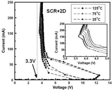
Fig. 9. Measured dc I–V characteristics of the ESD clamp device (SCR with two diodes in series) under different temperatures.
detection circuits and ESD clamp devices are fully silicided. In 3× VDD-tolerant ESD clamp circuit A, the widths of SCR in ESD clamp device are varied in 45 and 90 μm. On the other hand, the widths of SCR in ESD clamp device are varied in 30, 45, and 60 μm in 3× VDD-tolerant ESD clamp device B.
A. DCI–V Characteristics of ESD Clamp Device
The dc I–V characteristics of the ESD clamp device (SCR with two diodes in series) in 3 × VDD-tolerant ESD clamp circuit B is measured by using Tek370 curve tracer.
To avoid the issue of false triggering and latchup, the holding voltage of the SCR-based ESD clamp device with diodes in stacked configuration must be designed to be greater than the maximum voltage level of 3 × VDD (3.3 V in 0.13-μm CMOS process) under the normal circuit operating condition. The measured dc I–V characteristics of the ESD clamp device under different temperatures are shown in Fig. 9. The inset in Fig. 9 is the enlarged view around the holding points of one SCR with two stacked diodes in series (SCR + 2-D). The holding voltages of the ESD clamp device are 3.98, 3.82, and 3.64 V under the temperatures of 25 ◦C, 75◦C, and 125 ◦C, respectively. These holding voltages are higher than the voltage level of 3 × VDD (3.3 V) under the normal circuit operating conditions. Even if the ESD clamp device was mistriggered due to noise disturbance, it can be recovered to the normal condition after the noise source is removed. Therefore, the SCR-based ESD clamp device with a suitable number of stacked diodes in series can be safely applied in 3 × VDD-tolerant ESD clamp circuit without any latchup issue.
The measured dc I–V characteristics of the ESD clamp device under different substrate-triggered currents (I_trig) into the p+ trigger node are shown in Fig. 10. The measurement setup is also shown as the inset in Fig. 10. When the SCR-based ESD clamp device has no substrate-triggered current (I_trig = 0 mA), the SCR is essentially triggered on by junc-tion avalanche breakdown. As shown in Fig. 10, the trigger voltage of the fabricated SCR-based ESD clamp device without
Fig. 10. Measured dc I–V characteristics of the ESD clamp device (SCR with two diodes in series) under different substrate-triggered currents (I_trig).
the substrate-triggered current is as high as ∼12.4 V, which is higher than the breakdown voltage of the stacked NMOS with RESDin mixed-voltage I/O buffers. However, the trigger
voltage of the ESD clamp device is reduced to 8 V when the substrate-trigger current is 8 mA. Moreover, the trigger voltage of the ESD clamp device is reduced to only 4.2 V, which almost equals to the holding voltage of the ESD clamp device, when the substrate-triggered current is increased to 10 mA. The trigger voltage of the ESD clamp device is decreased while the substrate-triggered current is increased. ESD clamp device with low trigger voltage can be turned on more quickly to discharge ESD current to provide more effective protection for mixed-voltage I/O interfaces.
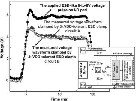
B. Turn-On Verification
The turn-on behavior of SCR devices is one of important factors for ESD protection, and it has been evaluated in some recent works [19]–[21]. To verify the turn-on efficiency of the proposed 3 × VDD-tolerant ESD clamp circuits, an experi-mental setup is shown as the inset in Fig. 11, where a voltage pulse generated from a pulse generator is used to simulate the rising edge of a PS-mode HBM ESD pulse. The voltage pulse generated from the pulse generator initially has a square-type voltage waveform with a rise time about∼10 ns and a pulse height of 6 V, as shown in Fig. 11. When the positive voltage pulse is applied to the I/O pad of the proposed ESD protection circuit with VSS grounded, the sharp-rising edge of the ESD-like voltage pulse will start the ESD detection to generate substrate-triggered current to trigger ESD clamp device on, and provide a low-impedance path between the I/O pad and VSS. The voltage waveform on the I/O pad is therefore clamped by the turned-on ESD clamp device. The voltage waveforms, clamped by 3× VDD-tolerant ESD clamp circuit A and B, on the I/O pad are also shown in Fig. 10. The voltage waveforms on the I/O pad are clamped by the Dp and ESD clamp device to ∼4 V, which is lower than the breakdown voltage of the stacked NMOS in the mixed-voltage I/O buffer. The time to clamp the 0-to-6 V voltage pulse to the holding voltage level
the I–V characteristic curve shifting over 20% from its original curve after three continuous ESD zaps at every ESD test level.
1) ESD Protection Design With 3 × VDD-Tolerant ESD Clamp Circuit A: The TLP-measured second breakdown
cur-rent and HBM ESD level of the I/O buffer with and without the proposed ESD protection design with 3 × VDD-tolerant ESD clamp circuit A under PS-mode ESD stress are compared in Table I. When the width of SCR device in ESD clamp device is 45 μm, the secondary breakdown current of the I/O buffer with the proposed ESD protection design and 3× VDD-tolerant ESD clamp circuit A can be increased from 0.2 to 4 A, as comparing with the I/O buffer without ESD protection. In addition, the HBM ESD level of the I/O buffer with the proposed ESD protection design can be improved from 500 V to 6 kV. When the width of SCR device in ESD clamp device is increased to 90 μm, the second breakdown current and HBM ESD level of the I/O buffer with the proposed ESD protection scheme can be further increased larger than 6 A and 8 kV, respectively. The proposed ESD protection design can significantly improve the second breakdown current and HBM ESD level of the 3× VDD-tolerant I/O buffer.
2) ESD Protection Design With 3 × VDD-Tolerant ESD Clamp Circuit B: The TLP-measured I–V characteristics of
the ESD clamp device with or without ESD detection circuit of 3 × VDD-tolerant ESD clamp circuit B under PS-mode ESD stress are shown in Fig. 12, where the width of the SCR in ESD clamp device is 60 μm. From the measured results, the trigger voltage of ESD clamp device without ESD detection circuit is 12.7 V, whereas the trigger voltage of ESD clamp device can be reduced to only 4.6 V by ESD detection circuit without involv-ing the junction avalanche breakdown. Therefore, the trigger voltage of ESD clamp device can be significantly reduced by the proposed ESD detection circuit to ensure effective ESD protection.
The second breakdown current and the turn-on resistance of the ESD protection circuit with a 60-μm-wide SCR and two diodes in series is 5.31 A and ∼1.9 Ω, respectively. The standby leakage current under 3.3-V bias of the whole ESD protection circuit is only 83 nA. By adjusting the width of the ESD clamp device and the size of the substrate driver in ESD detection circuit, the second breakdown current, turn-on resistance, and the trigger voltage of the ESD protection circuit can be modified to satisfy the specification of different mixed-voltage I/O circuits. The HBM ESD levels and MM ESD levels
Fig. 11. Measured voltage waveforms, clamped by 3× VDD-tolerant ESD clamp circuit A and B, on the I/O pad when a 0-to-6 V voltage pulse is applying to I/O pad under the PS-mode ESD stress (VDD floating and VSS grounded).
TABLE I
ESD ROBUSTNESS OFI/O BUFFERWITH ORWITHOUTESD PROTECTION
CIRCUITWITHESD CLAMPCIRCUITA
Fig. 12. Measured TLP I–V characteristics of the ESD clamp device in the 3× VDD-tolerant ESD clamp circuit B with or without ESD detection circuit under PS-mode ESD stress.
of the proposed ESD protection circuit with 3× VDD-tolerant ESD clamp circuit B with various widths of SCR-based ESD clamp devices under PS-mode ESD stress are listed in Table II.
TABLE II
ESD ROBUSTNESS OF THEPROPOSEDESD PROTECTIONCIRCUITWITH
ESD CLAMPCIRCUITB WITHVARIOUSWIDTHS OFESD CLAMPDEVICES
The HBM ESD levels of ESD protection circuit under ESD clamp device width of 30, 45, and 60 μm are 4 kV, 6.2 kV, and larger than 8 kV, respectively. Besides, the MM ESD levels of ESD protection circuit under ESD clamp device width of 30, 45, and 60 μm are 260, 380, and 440 V, respectively. The corresponding second breakdown current measured by TLP is also listed in Table II.
The CDM ESD robustness of the proposed ESD protection circuits are also verified by KeyTek RCDM tester. The 3 × VDD-tolerant I/O buffer protected by the proposed ESD protec-tion circuits in this paper (both 3× VDD-tolerant ESD clamp circuits A and B) can achieve a CDM ESD level of greater than
±1 kV.
V. PIN-TO-PINESD PROTECTION
In the whole chip ESD protection design, the proposed 3× VDD-tolerant ESD protection circuit can be shared with other 3× VDD-tolerant I/O buffers by connecting ESD bus to each other to achieve pin-to-pin ESD protection, as shown in Fig. 13. During the pin-to-pin ESD test, the ESD stress is applied to one I/O pad with other I/O pad grounded, where the VDD and VSS are initially floating. The ESD current will flow from one I/O pad through the forward diode Dp, ESD bus line, and then through the proposed 3× VDD-tolerant ESD clamp circuit to the VSS line, finally from the VSS line through the
Fig. 13. Shared ESD bus and 3× VDD-tolerant ESD clamp circuit for whole set of I/O buffers to achieve pin-to-pin ESD protection.
forward diode Dn to the other grounded I/O pad. Therefore, the pin-to-pin ESD protection can be achieved by using this ESD protection scheme with the proposed 3× VDD-tolerant ESD clamp circuit for 3× VDD-tolerant mixed-voltage I/O buffers.
VI. CONCLUSION
Two novel circuit solutions on ESD protection design, re-alized with 1 × VDD devices for mixed-voltage I/O buffer with 3× VDD input tolerance, have been successfully verified in two different 0.13-μm 1.2-V CMOS process. The four-mode (PS, NS, PD, and ND) ESD stresses and pin-to-pin ESD stresses on the 1.2/3.3-V mixed-voltage I/O buffer can be effectively discharged by the ESD protection scheme, with the proposed 3× VDD-tolerant power-rail ESD clamp circuits. The proposed 3× VDD-tolerant power-rail ESD clamp circuits operates without gate-oxide reliability issue under the normal circuit operating conditions. By using the special control circuit in the 3 × VDD-tolerant ESD clamp circuit B, the device sizes of the resistor, capacitor, and the substrate driver can be reduced. Therefore, the active area and the standby leakage current of the ESD detection circuit in 3× VDD-tolerant ESD clamp circuit B can be further reduced. In addition, the ESD detection circuit has also shown significant help on reducing the trigger voltage of ESD clamp device. The turn-on behaviors of the ESD clamp device have been measured to verify the effectiveness of the ESD detection circuit for both two 3 × VDD-tolerant ESD clamp circuits. The experimental results have also confirmed that the ESD robustness of the 3× VDD mixed-voltage I/O buffer can be significantly increased up to 8 kV with the proposed ESD protection designs. These two proposed power-rail ESD clamp circuit with the advantages of low leakage current, high ESD robustness, and no gate-oxide reliability issue are the excellent ESD protection solutions to
the mixed-voltage I/O interfaces with high-voltage input/output signals.
REFERENCES
[1] M.-D. Ker, S.-L. Chen, and C.-S. Tsai, “Overview and design of mixed-voltage I/O buffers with low-mixed-voltage thin-oxide CMOS transistors,” IEEE
Trans. Circuits Syst. I, Reg. Papers, vol. 53, no. 9, pp. 1934–1945,
Sep. 2006.
[2] Y. Luo, D. Nayak, D. Gitlin, M.-Y. Hao, C.-H. Kao, and C.-H. Wang, “Ox-ide reliability of drain engineered I/O NMOS from hot carrier injection,”
IEEE Electron Device Lett., vol. 24, no. 11, pp. 686–688, Nov. 2003.
[3] B. Serneels, T. Piessens, M. Steyaert, and W. Dehaene, “A high-voltage output driver in a standard 2.5 V 0.25μm CMOS technology,” in Proc.
IEEE Int. Solid-State Circuit Conf. Dig. Tech. Papers, 2004, pp. 146–147.
[4] W. R. Anderson and B. Krakauer, “ESD protection for mixed-voltage I/O using NMOS transistors stacked in a cascode configuration,” in Proc.
EOS/ESD Symp., 1998, pp. 54–62.
[5] J. Miller, M. Khazhinsky, and J. Weldon, “Engineering the cascoded NMOS output buffer for maximum Vt1,” in Proc. EOS/ESD Symp., 2000,
pp. 308–317.
[6] M.-D. Ker and K.-H. Lin, “Overview on electrostatic discharge protection designs for mixed-voltage I/O interfaces: Design concept and circuit im-plementations,” IEEE Trans. Circuits Syst. I, Reg. Papers, vol. 53, no. 2, pp. 235–246, Feb. 2006.
[7] M.-D. Ker and S.-L. Chen, “Mixed-voltage I/O buffer with dynamic gate-bias circuit to achieve 3× VDD input tolerance by using 1× VDD devices and single VDD supply,” in Proc. IEEE Int. Solid-State Circuits Conf. Dig.
Tech. Papers, 2005, pp. 524–525.
[8] T. Maloney and W. Kan, “Stacked PMOS clamps for high voltage power supply protection,” in Proc. EOS/ESD Symp., 1999, pp. 70–77. [9] S. S. Poon and T. Maloney, “New considerations for MOSFET power
clamps,” in Proc. EOS/ESD Symp., 2002, pp. 1–5.
[10] M.-D. Ker, W.-Y. Chen, and K.-C. Hsu, “Design on power-rail ESD clamp circuit for 3.3-V I/O interface by using only 1-V/2.5-V low-voltage devices in a 130-nm CMOS process,” in Proc. IEEE Int. Rel. Phys. Symp., 2005, pp. 606–607.
[11] M.-D. Ker, W.-J. Chang, C.-T. Wang, and W.-Y. Chen, “ESD protection for mixed-voltage I/O in low-voltage thin-oxide CMOS,” in Proc. IEEE
Int. Solid-State Circuits Conf. Dig. Tech. Papers, 2006, pp. 546–547.
[12] M.-D. Ker and C.-T. Wang, “ESD protection design by using only 1× VDD low-voltage devices for mixed-voltage I/O buffers with 3× VDD input tolerance,” in Proc. IEEE Asian Solid-State Circuits Conf., 2006, pp. 287–290.
complementary substrate-triggered SCR devices,” IEEE J. Solid-State
Circuits, vol. 38, no. 8, pp. 1380–1392, Aug. 2003.
[18] M.-D. Ker and C.-H. Chuang, “Electrostatic discharge protection de-sign for mixed-voltage CMOS I/O buffers,” IEEE J. Solid-State Circuits, vol. 37, no. 8, pp. 1046–1055, Aug. 2002.
[19] M.-D. Ker and K.-C. Hsu, “SCR device fabricated with dummy-gate structure to improve turn-on speed for effective ESD protection in CMOS technology,” IEEE Trans. Semicond. Manuf., vol. 18, no. 2, pp. 320–327, May 2005.
[20] J. D. Sarro, K. Chatty, R. Gauthier, and E. Rosenbaum, “Evaluation of SCR-based ESD protection devices in 90 nm and 65 nm CMOS technolo-gies,” in Proc. IEEE Int. Rel. Phys. Symp., 2007, pp. 348–357.
[21] G. Wybo, S. Verleye, B. V. Camp, and O. Marchial, “Characterizing the transient device behavior of SCRs by means of VFTLP waveform analysis,” in Proc. EOS/ESD Symp., 2007, pp. 366–375.
Ming-Dou Ker (S’92–M’94–SM’97–F’08) received
the Ph.D. degree from the Institute of Electronics, National Chiao-Tung University (NCTU), Hsinchu, Taiwan, in 1993.
He was the Department Manager with the VLSI Design Division, Computer and Communication Re-search Laboratories, Industrial Technology ReRe-search Institute, Hsinchu. Since 2004, he has been a Full Professor with the Department of Electronics En-gineering, NCTU. From 2006 to 2008, he served as the Director of Master Degree Program with the College of Electrical Engineering and Computer Science, NCTU, as well as the Associate Executive Director of the National Science and Technology Program on System-on-Chip (NSoC Office), Taiwan. In 2008, he was rotated to serve as the Chair Professor and the Vice President of I-Shou University, Kaohsiung, Taiwan. He has proposed many inventions to improve the reliability and quality of integrated circuits, which have been granted with 136 U.S. patents and 143 (Taiwan) patents. He had been invited to teach and/or to consult the reliability and quality design for integrated circuits by hundreds of design houses and semiconductor companies in the worldwide IC industry. In the field of relia-bility and quality design for circuits and systems in CMOS technology, he has published over 350 technical papers in international journals and conferences. His current research interests include reliability and quality design for nano-electronics and gigascale systems, high-speed and mixed-voltage I/O interface circuits, on-glass circuits for system-on-panel applications, and biomimetic circuits and systems for intelligent prosthesis.
Dr. Ker has served as a member of the Technical Program Committee and the Session Chair of numerous international conferences. He served as the Associate Editor for the IEEE TRANSACTIONS ONVLSI SYSTEMS. He has been selected as the Distinguished Lecturer in the IEEE Circuits and Systems Society (for year 2006–2007) and in the IEEE Electron Devices Society (since 2008). He was the President of Foundation in the Taiwan ESD Association. In 2005, one of his patents on ESD protection design has been awarded with the National Invention Award in Taiwan. In 2008, he has been elevated as an IEEE Fellow “for his contributions to the electrostatic protection in integrated circuits and the performance optimization of VLSI microsystems.”