行政院國家科學委員會專題研究計畫 成果報告
磁控濺鍍法製備 CIGS 太陽能電池成長與元件特性之研究
(I)
研究成果報告(完整版)
計 畫 類 別 : 個別型 計 畫 編 號 : NSC 98-ET-E-018-001-ET 執 行 期 間 : 98 年 01 月 01 日至 98 年 12 月 31 日 執 行 單 位 : 國立彰化師範大學機電工程學系暨研究所 計 畫 主 持 人 : 林義成 計畫參與人員: 碩士班研究生-兼任助理人員:陳永霖 碩士班研究生-兼任助理人員:柯佳宏 博士班研究生-兼任助理人員:嚴文材 處 理 方 式 : 本計畫可公開查詢 中 華 民 國 99 年 04 月 25 日行政院國家科學委員會/經濟部能源局
「能源科技學術合作研究計畫」成果報告
磁控濺鍍法製備 CIGS 太陽能電池成長與元件特性之
研究(I)
計畫類別:■ 個別型計畫 □ 整合型計畫
計畫編號:98-ET-E-018-001-ET
執行期間:98 年 01 月 01 日至 98 年 12 月 31 日
計畫主持人:林義成
計畫參與人員:嚴文材、陳永霖、柯佳宏
成果報告類型(依經費核定清單規定繳交):□ 精簡報告
█ 完整報告
本成果報告包括以下應繳交之附件:
□赴國外出差或研習心得報告一份
□赴大陸地區出差或研習心得報告一份
□出席國際學術會議心得報告及發表之論文各一份
□國際合作研究計畫國外研究報告書一份
處理方式:除產學合作研究計畫、提升產業技術及人才培育研究
計畫、列管計畫及下列情形者外,得立即公開查詢
□涉及專利或其他智慧財產權,
□一年█二年後可公開查詢
執行單位:國立彰化師範大學機電工程學系
中 華 民 國 九十九 年 三 月 三十一 日
摘要
本計劃中,利用共濺鍍方式分別濺鍍銅銦鎵硒四元化合靶(CIGS) 與硫化銦靶(In2S3)於蘇打玻璃基板上沉積五元銅銦鎵硒硫(CIGSS)薄 膜,再經由後退火處理使薄膜擁有(112)優選方位之黃銅礦相。其中濺 鍍過程中之基板溫度以及後退火處理中之退火溫度與退火時間為影響 薄膜成相之重要參數。故本計劃分別依基板溫度、退火溫度、與退火 時間之不同參數條件下製備不同參數之銅銦鎵硒硫薄膜,並針對其結 構、成分、光電特性等方面進行探討。此共濺鍍技術可有效應用於製 備大面積化且近化學當量比之銅銦鎵硒硫薄膜。CIGS 薄膜太陽能電池 吸收層研究顯示:本實驗室開發之新穎製程所得之CIGSS 薄膜,在基 板溫度473 K 及 763 K 之退火溫度下退火 5 分鐘,具有單一的黃銅礦 相態且其結晶性良好。電性分析結果得知此 CIGSS 吸收層電阻值為 45 Ωcm、載子濃度為 4.86×1016 cm-3,薄膜光學能隙值估計為1.18eV 左右。上述光電特性滿足目前開發中之 CIGS 薄膜太陽能電池吸收層 之要求。關鍵字:銅銦鎵硒硫、共濺鍍、四元靶、硫化銦、退火。
Abstract
Pentanary Cu(In,Ga)(Se,S)2 (CIGSS) films were deposited on soda
lime glass substrates by co-sputtering quaternary alloy, Cu(In,Ga)Se2 and
In2S3 targets followed by post-annealing. The key parameters, such as
substrate temperature (Tsub), annealing temperature (Tanneal), and annealing
time etc., on the structural, compositional, optical and electrical properties of CIGSS films were sequentially investigated. This technique was scalable to large-area devices with near-stoichiometry single-phase chalcopyrite CIGSS layers. In summary, the polycrystalline CIGSS films prepared by a novel co-sputtering process followed by substrate temperature of 473K, and with a post annealing at 763 K for 5 minutes shows good crystallinity with near-stoichiometry composition. The prepared CIGSS thin film has a chalcopyrite structure and improved crystallinity which has a resistivity of 45 Ωcm and carrier concentration of 4.86×1016 cm-3 with an optical band gap estimated to be around 1.18eV. These properties have shown to be satisfactory for the ideal CIGS thin film solar cells.
Keywords:Cu(In,Ga)(Se,S)2 (CIGSS); Co-sputtering; Quaternary target;
一、 前言
Each type of solar cells owns its advantages and disadvantages. Among these various solar cells, copper indium gallium diselenium (CIGS) got attention with the features of high potential for conversion efficiency, great stability, lowing materials cost, thin filmable, no toxic pollution usage like arsenic and cadmium elements, and shortage materials as silicon. Cu(In,Ga)Se2(CIGS) is Ⅰ-Ⅲ-Ⅵ2 compound semiconductor with
chalcopyrite structure and solar cells which use it as absorption layer are called “CIGS thin film solar cells”. Currently, the developments of techniques of thin film solar cells are highly concerned and Cu(In,Ga)Se2(CIGS) thin film solar cells are particularly interested due to
its outstanding performance on quantum efficiency and evolution potential. In 2008, National Renewable Energy Laboratory (NREL), announce that they break the world record for the quantum efficiency of CIGS thin film solar cells from 19.5%, which they kept before, to 19.9%, and this record is the highest among current thin film solar cells[1].
The CIGS thin film solar cells have high radiation resistence, long-term stability, and slight decline in quality during operating. Furthermore, the bandgap of ternary thin film, CuInSe2(CIS), is 1.04eV,
and with proper replacement of In or Se with Ⅲ(Ga) or Ⅳ(S) will form CIGS quaternary-polycrystal solid solution. This will make the bandgap of the material be various within 1.04eV~1.65eV and much more fitting with the solar spectrum. So, it is very suitable to modulate and optimize the bandgap of the material and let CIGS thin film solar cells have the best photonic bandgap which is proper for homojunction and heterojunction. Otherwise, the material is suitable for using as absorber layer of high-efficiency solar cell due to high optical absorption coefficient, p-n junction could obtain by modulating the composition, and long-term damp
heat stability.
There are two common processes to fabricate CIGS thin film solar cells: 1. multi-sources co-evaporation fabrication processes. 2. two-stage selenizations fabrication process. The first fabrications process using Cu, In, Ga and Se as separate elemental sources with Cu-rich first than Cu-poor. The advantage of this fabrication process is that the composition could control by evaporation time and sequence of Cu and Ga to modulate the optical bandgap and to achieve high quantum efficiency. Although, the quality of the films are excellent but the disadvantages is low utilizing rate of material, difficult to fabricate large-area cells, low evaporation rate, complex fabrication process, bad reconstruction property, expensive equipment, and currently not suitable for mass production. The second fabrication process using binary or ternary alloy target to deposit metal precursor and than selenization and vulcanization in the gas H2Se and H2S,
particularly. This fabrication process is fine for large-area cells. But according to the researches, CIGS thin film is very sensitive about the fabrication process of CIG precursor, which is affected by the composition and structure of CIG thin film. The disadvantages of this fabrication process is the industrial problems of highly toxic H2Se, low selenization
rate and temperature control in selenization process. So, sputter is the solution to achieve high homogeneity of absorption layer of CIGS thin film, low cost, good reconstruction and easy fabrication process.
二、 研究目的
Finally, the single-crystalline chalcopyrite absorber layers have reached a high performance level over the last years. There is still an urgent need to develop an industrial easily scalable deposition technology to obtain stoichiometric layers and its scalability for large area devices. We also propose an innovative co-sputtering process is presented using individual quaternary alloy, Cu(In,Ga)Se2 (CIGS) and In2S3 targets to
prepare pentanary Cu(In,Ga)(Se,S)2 (CIGSS) films. This technique is
easily reproducible and features in both energy and materials saving which is very suitable for large area deposition. By incorporating sulfur into the partly sulfurized CIGS films, we prepare graded band gap CIGSS layers with the ultimate aim for producing high efficient photovoltaic devices. In this work, single-phase CIGSS films were deposited on glass substrates by co-sputtering of quaternary CIGS alloy and In2S3 targets. The effects of
key parameters, such as substrate temperature while during deposition, and sequentially process like annealing temperature and time, and so on, were elucidated. In addition, the micro-structural, electrical, and optical properties of CIGSS films developing throughout the whole process were also extensively investigated.
三、 文獻探討
Cu(In,Ga)Se2 (CIGS) alloy, composed of the materials of CuInSe2
and CuGaSe2, is a semiconductor material which belongs to group
I-Ⅲ-Ⅵ2 and has the tetragonal chalcopyrite structure[2].The CuInSe2 of
chalcopyrite structure, it likes the Cu or In atom, displaces the Zn from ZnSe of which GroupⅡ- compound is derivatized from cubic sphalerite Ⅵ structure. Each atom in group I (Cu) or group III (In) comprises four bonding with Ⅵ(Se) atom. In other words, each Se atom has two bonding with Cu and two bonding with In. Some compounds in group II can be displaced by group I (Cu) or group III (In) to produce ternary compounds. When atoms Cu and In are regularly filled in the original atom positions of group II, the cations are arranged along c axis in order to make unit length of c axis, which developed into two times large of sphalerite structure which is two times larger and belongs to the tetragonal crystal system of chalcopyrite structure (See Fig. 1). This kind of structure presumed as two unit-cell of sphalerite structure stacked, yet its lattice constant c/a ratio is not equal to 2 due to a bond intensity difference between group I-Ⅵ and group Ⅲ-Ⅵ. On the contrary, weight 2-c/a (-0.01 for CuInSe2, +0.04 for
CuGaSe2) is obtainable from the tetragonal lattice distortion measurement
Fig. 1 (a) Zinc blende ZnSe lattice and (b) chalcopyrite unit cell for CuInSe2. [3]
Furthermore to observe CuInSe2, through the binary phase-diagram
of Cu2Se-In2Se3 shown by Fig. 2 [2], it is found to from an α-phase
chalcopyrite structure as the temperature reaches to 700℃ and the composition of its thin film has 5 mole% tolerance of variation error, in which it means that even though CIS thin film composition, there shows segregation from composition ratio of Cu: In: Se = 1: 1 : 2, it can still possess chalcopyrite structure with the same physical and chemical properties while remaining within its composition range. And normal Cu-rich CIS thin film are in p-type with low resistivity of conductive type due to the existence of Cu-In atom antisites CuIn and In-vacancy Vin defect.
As the composition of Se reach to 50% in In-rich CIS thin film, its electric properties are decided by In-Cu antisites InCu (a deep double donor) and
Cu-vacancy VCu (a shallow acceptor), and two electrically inverse defects
produces at the same time and cause the conductive properties of In-rich thin film in high compensation and high resistivity of n-type form [4].
Fig. 2 Pseudobinary cut Cu2Se-In2Se3 of the ternary phase diagram. [2]
The approximate 1eV bandgap of CuInSe2 is lower than ideal spectral
value of solar energy. The leading CuInSe2 solar cell are added with Ga to
form active absorber layer Cu(In,Ga)Se2 that increases bandgap of
absorber layer. While the bandgap of CuInSe2 is 1.04eV and bandgap of
CuGaSe2 is 1.68eV, the increasing bandgap of Cu(In,Ga)Se2 will be [5]
according to the following formula: Eg(x)=(1-x)Eg(CIS)+xEg(CGS)-bx(1-x)
x represents Ga content , 1-x represents In content, b value is 0.15~ 0.24eV.
3.1 Cu(In,Ga)Se2 deposition processes
Cu(In,Ga)Se2 (CIGS)-based thin film solar cells have been carried
out by various fabrication processes, including co-evaporation [6-7], sputtering [8-9], the selenization of precursors thin film [10-11], electrodeposition [12-13], and non-vacuum process [14-15]. Factors that
affect the process selection are the degree of control the process offers, material utilization, capital equipment costs and stability prospects. The most successful methods for depositing device quality films are co-evaporation and the selenization of metals and compound materials in a Se-containing atmosphere. The other techniques have not yet produced high efficiency devices and/or are not compatible with large-scale production. The most important features and advantages of the co-evaporation and selenization methods are reviewed below.
(1) Co-evaporation process
The co-evaporation method can be divided into one-step process, two-step process, and three-step process. This process is schematically illustrated in Fig. 3. For one-step process, the total element co-evaluate at substrate temperature of 450~550℃ at the same time. During the process of thin film deposition, it is necessary to adjust evaporation rate of each element; in the latter period of thin film deposition, enhance In deposition to guarantee In-rich thin film surface. The whole process is required to complete at one-step, for adjustment of process parameter involved are rather complicated and preparation processes are difficult to control. Mickelsen and Chen in The Boeing Company proposed a method of two step-process, of which the procedure is the so called the Boeing or bilayer process. The first step is to make a Cu-rich(Cu/In>1) CIS thin film (takes about 50.0%~66.7% of full thickness) deposition with low resistivity of p-type semiconductor at substrate temperature of 350℃. The second layer is to make a deposition of Cu-poor CIS thin film at high substrate temperature of 450℃ (CIGS thin film deposition, substrate temperature is 550℃), of which the thin film belongs to medium-high resistivity of n-type semiconductor, forming a graded p-type semiconductor through diffusion between two layers [16-17].
Fig. 3 Schematic co-evaporation process.
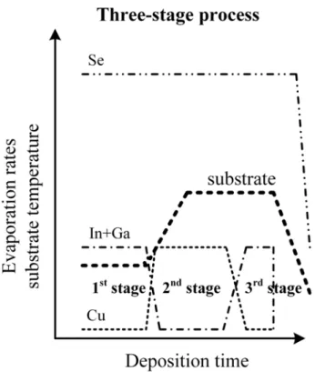
The National Renewable Energy Laboratory (NREL) adopts a three-step process of CIGS thin film with high conversion efficiency [18]. This process is schematically illustrated in Fig. 4. In the first stage, the precursor (In,Ga)2Se3 layer formed by the co-evaporation of In,Ga and Se
at substrate temperature of 300℃. In the second stage, the Cu and Se are co-evaporated to bring the overall composition slightly Cu-rich at substrate temperature of 560℃. Between the second and the third stage, the substrate is under the Se flux while ramping up the temperature. In the final step, the film is driven Cu-poor to form what is presumed to be the alloy-equivalent of the OVC (OVC is the compound with ordered vacancies) layer by exposing it to a flux of (In,Ga)2Se3 at 560°C followed
by a cool-down in Se vapor. The copper indium gallium diselenide thin-film solar cell recently reached 19.9% efficiency [1], setting a new world record for this type of cell.
Fig. 4 Schematic of NREL' three stage process.
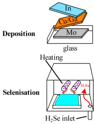
(2) Selenization of metallic precursor layers
The selenization process can be divided into two steps: the first-step is to deposit precursor layer like Cu-In or Cu-In-Ga at substrate temperature of 200℃; the second step is to perform heat treatments to precursor layer under atmospheres of H2Se/H2S+Ar or Se/S[19]. This
process is schematically illustrated in Fig. 5. The advantages of selenization process are non-existence of high-temperature deposition, easy to control elemental stoichiometric of thin film, film thickness, and uniform distribution of its compositions, low requirements for equipments. The process has become the top choice process of current commercial industry. Deposition of precursor layer includes vacuum and non-vacuum processes. The vacuum process includes evaporation or sputtering deposition of Cu-In-Ga stackings with Se or not, alloys or compounds. non-vacuum process mainly includes electrodeposition, spray pyrolysis, and chemical spray, ect. During selenization process, H2Se is the best Se
source, but its biggest drawback is the toxicity and strong evaporation, which requires high pressure vessel for storage. Se pressure is difficult to control as taking solid Se as Se source. Especially in the process during heat treatment, it will cause loss of element such as In or Ga. Many problems exist in mass production, but no toxicity problems exist. The organometallic Se source ((C2H5)Se2:DESe) is hopeful of becoming the
selenide displacement of toxic H2Se[20], which is under study and cost
accounts processes for a lot.
Fig. 5 Schematic selenization process used H2Se to selenize a metal stack
precursors.
Honda Motor Company, Japan in Feb, 2008 displays its patented process [21], which its innovative step includes three-stage selenization process, sodium coating process, etc. Low-alkali glass is adopted as substrate because of its softening point is much higher than soda-lime glass, while enhanced selenization temperature can improve CIGS
crystallinity. The superiority of CIGS crystallinity performing on the substrate as adopting sodium doped glass that makes Honda start using car coating sprayer to perform sodium-containing solution coating. Selenization precursor layer adopts sputtering deposition to produce stacked precursor layer (In and Cu-Ga), and then uses three-stage selenization process to create precursor layer, in which thermal diffusivity process is rising from room temperature to 250℃; CIGS crystallization process is rising from 250℃to 450℃; recombination process of CIGS crystal structures is from 450℃to 650℃. Three-stage selenization process obtains the advantages of uniform composition distribution, good crystallinity, and larger grain size, etc. Honda Motor Company reaches 11.2% in average conversion efficiency of large-area cell modules (79.1cm×141.7cm =11,208 cm2) in 2009.
Factors that affect the process selection are the degree of control the process offers, material utilization, capital equipment costs and stability prospects. The most successful methods for depositing device quality films are co-evaporation and the selenization of metals and compound materials in a Se-containing atmosphere, some issues remain unsolved. Co-evaporation is the conventional technique applicable to laboratory fabrication. However, the process complexity and high production costs impede the further development. Consequently, researchers still endeavor to overcome the difficulty in scaling up for large scale manufacturing. In view of this, an innovative co-sputtering process is presented using individual quaternary alloy, Cu(In,Ga)Se2 (CIGS) and In2S3 targets to
prepare pentanary Cu(In,Ga)(Se,S)2 (CIGSS) films. This technique is
easily reproducible and features in both energy and materials saving which is very suitable for large area deposition. By incorporating sulfur into the partly sulfurized CIGS films, we prepare graded band gap CIGSS layers
with the ultimate aim for producing more efficient photovoltaic devices. In this study, single-phase CIGSS films were deposited on glass substrates by co-sputtering of quaternary CIGS alloy and In2S3 targets. The effects of
key parameters, such as substrate temperature and annealing time etc., were elucidated. In addition, microstructural, electrical, and optical properties developing throughout the whole process were also extensively investigated.
四、 研究方法
The CIGSS precursor film comprised of a Cu-rich/In-rich bi-layer structure were deposited on soda lime glass substrates by RF (for CIGS alloy target) and DC (for In2S3 target) magnetron co-sputtering technique.
The targets were circle disks 76.2 mm in diameter with a composition of Cu/In/Ga/Se =25/17.5/7.5/50 at.% (quaternary alloyed CIGS target) and In/S=40/60 at.% (In2S3 target), respectively. Substrates were ultrasonically
cleaned in organic solvents. The sputtering chamber was evacuated to 6.65×10⁻⁴ Pa by a turbo molecular pump. Argon was admitted as the sputtering gas. Before deposition, both the CIGS and In2S3 targets surface
were cleaned by pre-sputtering with argon plasma for 5 min. The RF power of 125 W was applied to CIGS target. While for In2S3 target, a DC
power of 50 W was employed.All CIGSS precursor films were 1.0 μm in thickness and deposited under a working pressure of 0.67 Pa.
The total experiment would be divided into three sections. In the first section, to evaluate the phase formation, the substrate temperature was adjusted from ambient temperature to 523 K, and we preliminary discussed about the structural and morphologies of CIGSS precursor layers. Then in the second section, base on the above CISS precursor layer conditions, the as-deposited films were post-treated under argon atmosphere at 133 Pa by a two-step annealing process to tailor the band structure. During the first stage, the pretreatment temperature was linearly increased to 573 K at a given heating rate and maintained at that temperature for 40 minutes. During the second stage, the annealing temperature (Tanneal) was set to 733 K, 763 K, 793 K, 823 K and 853 K,
respectively and kept at that temperature for 15 minutes to investigate the annealing temperature affect the CIGSS films on the structural,
compositional, optical and electrical properties. Finally, in the last section, we base on the first and second section, and further discuss with the annealing time on the CIGSS films.
The resultant CIGSS films were characterized by the α-step profiler to determine the deposition rate and thickness of the films. A depth profile analysis was carried out by secondary ion mass spectroscopy (SIMS) to confirm the distribution of constituent elements along the CIGSS absorbers, the crystallographic properties of the CIGSS films was investigated by X-ray diffraction (XRD) using CuKα (λ=1.5405 Å) radiation while the surface morphology and composition were investigated by scanning electron microscope (SEM) and Energy dispersive X-ray spectroscopy (EDS). The electrical properties of the films were evaluated by a standard four-point probe and Hall measurements. Finally, a UV/VIS/NIR spectrophotometer was employed to study the optical properties of the films.
五、 結果與討論
5.1 Effects of substrate temperature on the compositional and structural properties of CIGSS precursor films
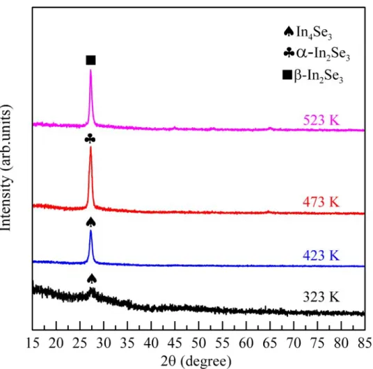
XRD patterns reveal information on phase transformation for CIGSS films. Firstly, to study the effect of substrate temperatures (Tsub), all
samples under investigation were co-sputtered at given Tsub. The results
shown in Fig.6 indicated that amorphous CIGSS precursor films is dominant as Tsub = 323 K. Subsequent melting of indium at 423 K resulted
in the formation of In4Se3 phase accompanied by the improved
crystallinity of the CIGSS films. As Tsub exceeded the melting point of
selenium, the In4Se3 phase disappeared. This could be explained by that
the mobile selenium atoms facilitate the decomposition of In4Se3. In
contrast, as Tsub further increased to 473 K, the α-In2Se3 phase emerged.
Eventually, β-In2Se3 was thriving at Tsub = 523 K. The phase evolution
presented in Fig.6 is coincident with those reported elsewhere [22]. The composition of above samples as determined by EDS is listed in Table 1. By sampling at four different regions on the film surface, all experimental data are presented as an average of the atomic percentage of each element. Coincident with our expectation, the results shown in Table 1 and Fig.4a have proved that all CIGSS films exhibit an In-rich structure. In addition, the atomic ratios of Ga/(In+Ga) and Cu/(In+Ga) are almost constant with values of 0.16 and 0.70, respectively regardless of the substrate temperature. This fact also agrees with the literature [23].
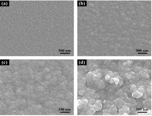
The surface morphologies of CIGSS precursor films deposited at different substrate temperatures is exhibited Fig. 7. It shows that initially, densely packed conical nanoparticles were distributed uniformly on the surface at Tsub = 323 K. Due to the limited surface diffusion of sputtered
atoms, the morphology of the as-deposited films (Fig. 7a) resembles to the Zone I area in the Thornton structural zone model [24]. A higher substrate temperature implies an improved surface atoms mobility. Consequently, these nanoparticles started to agglomerate and the grainy morphology disappear which, in turn, reduced the grain boundaries defects. As a result, a smooth surface with tiny amounts of voids appeared as indicated in Fig. 7b~7c. A drastic change in the film morphologies in Fig.7d could be attributed the phase transformation at Tsub =523 K as detected by XRD in
Fig.1 by the variation in compositions of the deposited films [25].
5.2 Effects of post annealing temperature on CIGSS film properties
Annealing is a prerequisite tool to prepare the desired chalcopyrite compound which acts as an absorber layer in high-efficiency thin film solar cells. For improving the graded band structure of the CIGSS precursor layers, a two-step post annealing is employed in this section 5.2, and the details of precursor CIGSS sample before annealing treatment that basic on discussion of the section 5.1.
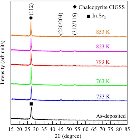
X-ray diffraction patterns (Fig.8) show that the as-deposited CIGSS precursor films comprised of binary selenide (In4Se3) phase were
transformed to chalcopyrite structure with a preferred orientation in the (112) plane after undergoing a two-step post-annealing. Only the peaks locating at 27.18o, 45o, and 52.89o were appeared, which corresponds to the (112), (220)/(204), and (312)/(316) crystal planes, respectively. As the annealing temperature increased to 763 K, the peak intensity of the (112) plane goes to its maximum owing to the improved crystallinity. If the annealing temperature was higher than 763 K, the intensity of the (112) plane fell off. This could be attributed to the pin-holes and defects
formation within the films. The cracks resided in the surface as the annealing temperature exceeded 763 K were shown in Fig.11 (e),(f). It is worthy to note that the position of the (112) diffraction peak shifted slightly to lower diffraction angles at higher annealing temperatures as the result of sulfur percolation into the CIGS films at different concentration level. At higher annealing temperatures, less amount of volatile sulfur was incorporated into the films, thus the deformation of crystal structures was weaken. Therefore, the corresponding lattice constant approach to the value of stoichiometric Cu(Ga,In)Se2 films [26].
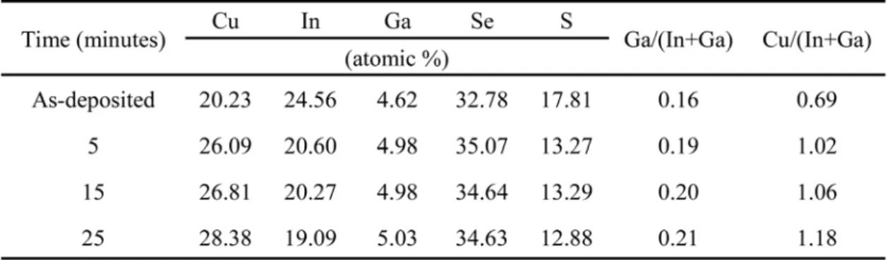
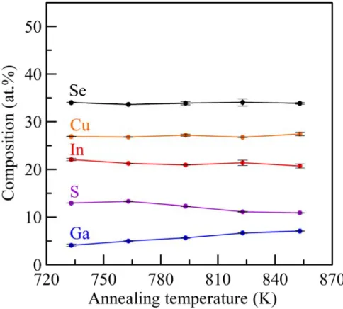
Table 2 list the compositions of the CIGSS films post-annealed at different Tanneal. Besides, the concentration profile of each constituent
element was depicted in Fig.9. It shows that the indium and sulfur content in the resultant CIGSS films decreased from 24.66 to 20.73% and from 18.01 to 10.89%, respectively. This could be ascribed to the lower melting point of both indium (430 K) and sulfur (392 K) as compared to other constituent elements in the films. At higher annealing temperatures, the mobile indium and sulfur atoms are more liable to escape from the chalcopyrite structures by vaporization. In addition, the unstable InxS (x>1)
is likely to appear in the gas phase [27-28] owing to the indium-rich nature of the as-deposited CIGSS thin films at high annealing temperatures. Accordingly, the composition of both elements decreased considerably at high annealing temperatures [29-30]. In contrast, owing to the high melting point of copper (1356 K), the variation in concentration was relatively small. The SIMS analysis in Fig. 10(b) indicates that sulfur has a uniform depth profile at elevated temperatures in comparison to other counterparts owing to its higher diffusivity. In general, for a high efficiency CIGS solar cell the atomic ratio of Cu:(In+Ga) varies from 0.95 to 1.05 [31-32]. For the CIGSS films prepared in our co-sputtering system,
this ratio was close to 1:1 regardless of the annealing temperatures. Furthermore, the near stoichiometric CIGSS films turn to be weak p-type semiconductor which is suitable as thin film solar cells materials.
To confirm the effect of post annealing on the variation in composition along the film depth, a SIMS depth profile (Fig. 10a) of the CIGSS precursor film was compared with that of CIGSS film annealing at 763 K (Fig. 5b). In Fig.10a, two distinct regions, designated as region (I) & (II), were divided by an abrupt boundary appearing at sputtering time of 400 seconds. Initially, an indium-rich region (I) exists underneath the film surface in which the constituent elements of indium, gallium and sulfur are at higher concentration level. In contrast, in the copper-rich region (II), both the concentrations of copper and selenium are higher than those in the region (I) while the concentrations of other components drop suddenly. The discontinuity in concentration profile is apparently an obstacle to establish the built-in graded band gap structure. After annealing at 763 K for 5 minutes, the concentration profile of each constituent element has changed drastically as shown in Fig.10b. The linear distribution profile of copper in CIGSS precursor film has turn to be downward arc with minimum value happening at sputtering time of 200 seconds. Besides, the selenium distributes evenly throughout the films whereas the concentration profiles of the remaining indium, gallium and sulfur exhibit characteristic features for graded band gap materials [33]. The unique distribution profile might be attributed to the enhanced kinetic energy for each constituent element by post annealing treatment. Therefore, the mobile atoms driving by the initial concentration gradient shown in Fig. 9a, are liable to be re-distributed effectively.
The morphology of the as-deposited CIGSS precursor films (Fig. 11a) exhibited a smooth surface comprised of compact nanoclusters with
diameter ranging from 100-150 nm. After post-annealing, the energetic surface particles are mobile more or less. This resulted in the formation of more compact films with improved crystallinity, as evidenced by the X-ray diffractograms in Fig. 8. Besides, the escaping of indium and sulfur atoms after post annealing leaves behind abundant of pin-holes as shown in Fig. 11b~d. As Tanneal = 823 K which approaches the softening temperature of
soda-lime glass substrates [34-35], the resultant residual thermal stress induces the peeling of deposited films. Accordingly, the crystallinity of the CIGSS films is deteriorated [36], as shown in Fig. 8. In addition, the volatile indium is liable to react with selenium and/or sulfur at high concentration level in the CIGSS films (Table 2) by forming binary selenides (In2Se or In2S) in the gas phase during the annealing process. An
increase in Tanneal implies a rise in the amount of pin-holes and surface
defects owing to the incorporation of binary selenides, In2Se3 with the
reactive copper atoms at high annealing temperature.
The surface roughness of CIGSS films is critical in high efficiency photovoltaic devices. A CIGS absorber layer with larger surface roughness is more susceptible to provide a shunt path between the incomplete coverage onto the CdS buffer layer that leads to the formation of undesirable heterostructures [37]. The AFM topography images are exhibited in Fig. 10 for CIGSS films annealing at various temperatures. The CIGSS precursor film has a loosely packed surface. However, the film annealed at 763 K is most rugged (Fig. 12c), with a root mean square (RMS) surface roughness of 8.0 nm. This could be ascribed to the escaping of volatile constituent elements, such as indium, sulfur, etc. For more high annealing temperature, the RMS-surface roughness decreased as shown in Fig. 12d~f. This could be attributed to the increased mobility of surface species at higher annealing temperature which, in turn, reduced
the surface roughness.
Fig. 13 shows the optical transmittance for CIGSS films annealed at various temperatures. All spectra exhibit characteristic of interference due to the non-uniformity in film thickness. The absorption coefficient, α, near the absorption edge was determined from the optical transmission measurements at various wavelengths using the relationship [38]
) I I ln( t 1 α= o (1)
Where t is the film thickness and Io and I are the intensities of the initial
and transmitted beams, respectively. Since the films are direct-gap semiconductors, their optical band gap (Eopt) can be described by the Tauc
relationship as following: 1/2 opt) E k(hν αhν= − (2)
Where α is the optical absorption coefficient, hν is the photon energy, and
k is the proportional constant. An extrapolating of the linear plot of
(αhν)2on the y-axis versus photon energy (hν) on the x-axis produces a value of Eopt at (αhν)2=0. Fig. 14 shows the optical band gaps obtained by
this way. All values range between 1.15~1.18 eV, which is in good agreement with those reported in the literature [39]. The optical band gap is broadened as the annealing temperature increased from 733 K and reached a maximum value of 1.18 eV (on average) at 763 K. Afterward, the optical band gap red-shifted at higher Tanneal and finally dropped to
1.15 eV at 823 K as the result of reduction in composition of sulfur and selenium at this temperature. Furthermore, in refer to Table 2, it also showed that the non-stoichiometric CIGSS films are more prone to secondary phase formation with a narrower optical band gap. A similar behavior was observed in CuInSe2 films deposited by magnetron
sputtering [40].
The electrical properties of the CIGSS films were characterized by Hall-effect measurement using the Van der Pawn geometry. Figure 15 indicates that all the near-stoichiometric CIGSS films annealed at various temperatures exhibit an ideal p-type semiconductor character [31-32]. Apparently, the resistivity of the films is higher at elevated annealing temperature. In contrast, an increase in the annealing temperature implies a decrease in carrier concentrations which is responsible for the appearance of pin-holes and surface defects in the vicinity of grain boundaries at higher annealing temperature as evidenced by Fig. 11. In contrast, the XRD and SEM results indicate coincidently that the polycrystalline CIGSS films with optimal crystallinity are obtained at an annealing temperature of 763 K where the carrier concentrations and the resistivity of the films are 4.86×1016 cm-3and 32 Ωcm, respectively.
5.3 Effects of post annealing time on CIGSS film properties
Here now we focus on the effect of annealing time during the second stage as the annealing temperature was increased to 763 K. The effect of annealing time on the microstructure, compositional, electrical, and optical properties of CIGSS films was extensively investigated in this section. The XRD patterns in Fig. 16 clearly show that all the films exhibited a chalcopyrite structure with well-resolved preferred orientation in the (112) diffraction plane. At an annealing time of 5 minutes, only the chalcopyrite phase was detected. Binary selenides phases, for example, InSe, CuSe and CuS onset as the annealing time extended to 25 minutes. The abundant content of selenium and sulfur in the as-deposited CIGSS films facilitates the alloying of each element with copper and indium, respectively at sufficient annealing time. The presence of binary selenides phases might
be deduced indirectly from the Cu-rich profile in CIGSS films. In this case, the post annealing treatment at a shorter interval of 5 minutes will suffice for optimal chalcopyrite structure with better crystallinity.
Table 3 shows the variations in chemical composition determined by EDS for the CIGSS films post annealing at different annealing time. It is worthy to note that the atomic ratio of Ga/(In+Ga) close to 0.2 is almost independent to the annealing time [41]. Accordingly, a decrease in indium content resulted in an increment in Cu/(In+Ga) for the post-annealed CIGSS films. This was attributed to the unstable InxS (x>1) evaporated
phase [27-28] which forms easily as the annealing time is extended and motivates the indium and sulfide content deficit [29-30]. In light of these results, we concluded that the near-stoichiometric CIGSS films were prepared by post-annealing at an annealing time of 5 minutes. Under this condition, binary selenides cannot be observed which agrees with those described in XRD analysis (Fig.16).
SIMS depth profiles of the CIGSS films are demonstrated in Fig. 17 to confirm the changes in composition and to investigate the effect of post annealing. Both the precursor film deposited at Tsub = 423 K and the
CIGSS film post annealed at 763 K for 5 minutes are compared. For CIGSS precursor film, the SIMS profile in Fig.17a reveals two distinct regions, designated as region (I) & (II), divided by an abrupt boundary appearing at sputtering time of 400 seconds. Firstly, an indium-rich region (I) exists underneath the film surface in which all the compositions of indium, gallium and sulfur are at higher concentration level. In contrast, in the copper-rich region (II), both the concentrations of copper and selenium are higher than those in the region (I) while the concentrations of other constituents drop suddenly. The discontinuity in concentration profile is apparently an obstacle to establish the built-in graded band gap structure.
Consequently, a surface sulfurization treatment by post-annealing is applied to facilitate graded band gap formation. After annealing at 763 K for 5 minutes, the concentration profile of each constituent element has changed drastically as shown in Fig.17b. Firstly, the linear distribution profile of copper is rounded to oval shape. Besides, the selenium distributes evenly throughout the films whereas the concentration profiles of the remaining indium, gallium and sulfur exhibit characteristic features for graded band gap materials [33]. There are attributed to the fact that annealing treatment enhanced the kinetic energy of each constituent element of CIGSS films. Therefore, the mobile atoms driving by the initial concentration gradient shown in Fig.17a are liable to be re-distributed effectively.
SEM micrographs (Fig. 18) compare the morphology of CIGSS films identical to those in Fig.16. It clearly shows that after annealing, nanoparticles up to a few hundred nanometers in diameter are agglomerated and densely packed throughout the surface. Owing to the energetic mobile particles with longer diffusion length, a smooth and compact surface appears after post-annealing. Figure 19 shows the dependence of optical transmittance at different annealing times for CIGSS films identical to those in Fig.16. All spectra exhibit characteristic of interference due to the non-uniformity in film thickness. An increase in annealing time implies significantly improving of optical transmittance in the infrared region (800~1800 nm). The absorption coefficient, α for a given sample is defined by the following relationship [38] and the optical band gap (Eopt) for a direct-gap
semiconductor is described by the Tauc relationship as follows:
) I I ln( t 1 α= o (1)
1/2 opt)
E k(hν
αhν= − (2)
The optical band gaps obtained graphically in Fig.20 show that all films have values between 1.13~1.18 eV, which is in good agreement with those reported in the literature [39]. Generally, the shift in optical band gap is related to the sulfur and selenium content of CIGSS film. An increase in the sulfur and selenium content results in shrinking of lattice constant, which subsequently blue-shifted the optical band gaps. However, as the annealing time lasts longer, the Eopt drops to ~1.13 eV. This effect was
responsible to the significant loss of sulfur and selenium by post annealing at 763 K for longer period as evidenced in Table 1. Furthermore, the thermal diffusion length at different annealing time was also susceptible to the variations in composition profiles which subsequently, lead to the optical band gap shifting.
The electrical properties of CIGSS films were derived by Hall effects measurement conducting at room temperature by van der Pauw geometry. All samples are identical to those in Fig.16. The dependence of resistivity, Hall mobility, and carrier concentration on the annealing time is sketched in Fig.8. It shows that binary selenides appearing at longer annealing time contribute to the raising in carrier concentration as evidenced in Fig.16 [37]. Accordingly, the resistivity of CIGSS films is dropped off. A closer inspection proposed that the increment in carrier concentration for longer annealing time (15~25 minutes) is deduced from the increase of the Cu/(In+Ga) ratio as shown in Table 3, which renders more abundant interstitial Cu atoms. As referred elsewhere [42-43], the resistivity of CIGSS films will slightly decline due to the existence of bulk defects in the CIGSS absorber appearing at higher annealing temperatures for longer annealing times. However, all the CIGSS films annealing with different time periods will finally turn to be p-type semiconductor materials.
六、 結論
In this study, p-type chalcopyrite CIGSS films were deposited on soda lime glass substrates by a novel co-sputtering technique using individual quaternary alloy, Cu(In,Ga)Se2 and In2S3 targets followed by
post-annealing treatment. This technique is easily reproducible and features in both energy and materials saving which is very suitable for large area deposition in producing more efficient photovoltaic devices. And in the conclusion, we still divided into three parts to list about the conclusion of each section.
Substrate Temperature:
At first, a co-sputtering CIGS precursor films deposited at various substrate temperatures were prepared. Experimental results indicated that amorphous CIGSS films is dominant as Tsub.=323 K. Subsequent melting
of indium at Tsub.=423 K resulted in the formation of In4Se3 phase while
the crystallinity of the film was improved. As Tsub.=473 K, the α-In2Se3
phase emerged. Eventually, β-In2Se3 appeared as Tsub.=523 K. All CIGSS
films exhibit an In-rich structure as evidenced by EDS analysis. In addition, the atomic ratios of Ga/(In+Ga) and Cu/(In+Ga) are almost constant with values of 0.16 and 0.70, respectively regardless of the substrate temperature. The surface morphologies of the as-deposited CIGSS films resemble to the Zone I area in the Thornton structural zone model.
Annealing temperature:
For better performance, a CIGSS precursor films co-sputtered at Tsub.= 473 K are chose as samples to employ post-annealing treatment
annealing temperature on the structural, electrical, and optical properties of CIGSS films were extensively investigated and concluded that:
1. The as-deposited CIGSS precursor films were mainly comprised of In4Se3 phase with no sign of chalcopyrite structure. After two-step
post annealing, the XRD patterns reveals that all the CIGSS films exhibited sharp crystallinity chalcopyrite peaks with a preferred orientation along the (112) plane. Furthermore, the position of the (112) peaks slightly shifted to lower diffraction angles as the annealing temperature increased.
2. EDS profile shows that the ratios of each constituent element were near stoichiometry after post-annealing. The SIMS depth profiles reveal an enhanced diffusivity at an annealing temperature of 763 K. 3. As the annealing temperature is higher than 823 K, which is close to
the softening temperature of soda-lime glass substrates, the films peeled off due to the residual thermal stress. At this temperature, the crystallinity of the CIGSS films also began to deteriorate.
4. Polycrystalline CIGSS films with the best crystallinity were obtained at an annealing temperature of 763 K, with a carrier concentration and film resistivity of 4.86×1016 cm-3and 32 Ωcm, respectively. The optical band gap of the CIGSS absorber layer was estimated to be 1.18 eV.
Annealing time:
To improve the graded band structure, a CIGSS precursor films co-sputtered at Tsub.= 473 K and the annealing temperature was set at
763 K to employ post-annealing treatment with various annealing time.
1. The XRD patterns clearly show that all the resultant films exhibited a chalcopyrite structure with well-resolved preferred orientation in the (112) diffraction plane. Binary selenides phase onset as the annealing time extended to 25 minutes. Therefore, a shorter interval of 5 minutes will suffice for optimal chalcopyrite structure. SIMS depth profiles reveals two distinct region divided by an abrupt boundary. First, an indium-rich region (I) exists underneath the film surface in which all of the compositions of indium, gallium and sulfur are at higher concentration level. In contrast, in the copper-rich region (II), both the concentrations of copper and selenium are higher than those in the region (I) while the concentrations of other constituents drop suddenly.
2. The optical transmittance in the infrared region (800~1800 nm) is improved significantly as the annealing time increased. All films have Eopt lying between 1.13~1.18 eV. As the annealing time is longer than
25 minutes, the Eopt dropped to ~1.13 eV. This effect was caused by
the significant loss of sulfur and selenium after the CIGSS precursor films were annealed at 763 K for longer period.
In summary, the polycrystalline CIGSS films prepared by a novel co-sputtering process followed by substrate temperature of 473K, and with a post annealing at 763 K for 5 minutes shows good crystallinity with near-stoichiometry composition. The CIGSS film has optimal value of carrier concentrations, 4.86×1016cm-3 and resistivity of 45 Ωcm, respectively.
List of table captions
Table 1. Dependence of the composition determined by EDS for CIGSS films deposited at different substrate temperatures.
Table 2 EDS data of as-deposited and CIGSS films annealed at different temperatures.
Table 3.EDS analysis of CIGSS films annealed at 763K for different annealing time.
List of figure captions
Fig. 6 XRD diffraction patterns of CIGSS films deposited at different substrate temperatures.
Fig. 7 Surface morphologies of CIGSS thin films deposited at different substrate temperatures of (a) 323 K, (b) 423 K, (c) 473 K, and (d) 523 K.
Fig. 8 X-ray diffraction patterns of CIGSS films before and after annealing at different temperature.
Fig. 9 Dependence of the composition determined by DES for CIGSS films at different annealing temperatures.
Fig. 10 SIMS depth profile of an as-deposited CIGSS films (a) and one annealed at 763K (b).
Fig. 11 SEM morphologies of CIGSS films annealed at different temperatures: (a) as-deposited, (b) 733 K, (c) 763 K, (d) 793 K, (e) 823 K, and (f) 853 K.
Fig. 12 AFM micrograph of CIGSS films annealed at different temperatures: (a) as-deposited, (b)733 K, (c)763 K, (d)793 K, (e) 823 K, (f) 853 K.
Fig. 13 Transmittance plots of CIGSS films as a function of annealing temperature.
Fig. 14 Plot of (αhν)2 versus photon energy for CIGSS films as a function of annealing temperature.
Fig. 15 The resistivity, hall mobility, and carrier concentration of the CIGSS films that as a function of annealing temperature.
Fig. 16 X-ray diffraction patterns of CIGSS films annealed at 763 K for different annealing time.
Fig. 17 SIMS depth profile of CIGSS films deposited at 423 K (a) and annealed at 763 K for 5 minutes (b).
Fig. 18 SEM morphologies of CIGSS films annealed at 763 K for different times: (a) 5 minutes, (b) 15 minutes, (c) 25 minutes.
Fig. 19 Transmittance plots of CIGSS films annealed at 763 K for different annealing time.
Fig. 20 Plot of (αhν)2 versus photon energy for CIGSS films annealed at 763 K for different annealing time.
Fig. 21 Resistivity, Hall mobility, and carrier concentration of CIGSS films annealed at 763 K for different annealing time.
七、 計畫成果自評
研究成果概述 本計畫係從2009 年 1 月開始,迄 2009 年 12 月底結束。回顧這一 年多的時間裡,本研究團隊成員無不卯足全力積極研發。過去一年多 的表現,相關的成果數據如下表所示。檢視過去一年的表現,本研究 團隊認為除元件效率尚未能達成設定目標外,更積極投稿期刊論文。 學術性期刊1. W. T. Yen, Y. C. Lin*, P. C. Yao, J. H. Ke and Y. L. Chen, 2009, “Growth characteristics and properties of ZnO:Ga thin films prepared by pulsed DC magnetron sputtering” Applied Surface Science 256 (2010) 3432-3437, (SCI).
2. W. T. Yen, Y. L. Chen, J. H. Ke, Y. C. Lin*, C. Y. Nieh and S. C. Liang, 2009, “The study of surface sulfurization to improve pentanary Cu(In,Ga)(Se,S)2 films by co-sputtering quaternary alloy and In2S3
targets” Thin Solid Films, (Submitted) (SCI).
3. W. T. Yen, Y. C. Lin*, P. C. Yao, Y. L. Chen, J. H. Ke, and S. T. Hang, 2009,“Influence of annealing temperature on properties of Cu(In,Ga)(Se,S)2 thin films prepared by co-sputtering from quaternary
alloy and In2S3 targets” Vacuum, (Submitted) (SCI).
研討會論文
1. Wen-Tsai Yen(嚴文材), Jia-Hong Ke (柯佳宏), Yi-Cheng Lin (林義 成), Cuo-Yo Nieh (倪國裕), Shih-Chang Liang (梁仕昌), Hsiao-Min Wu ( 吳 曉 旻 ), “Study of molybdenum thin films prepared for Cu(In,Ga)Se2 solar cells back contact using DC magnetron sputtering”,
Acceptance Letter of your abstract submitted to TACT 2009
培養研究生 博士班學生:嚴文材 碩士生學生:陳永霖、柯佳宏 本計畫研發成 果 自 評 表 成果項目 計畫達成情形 國 內 提出申請 0 件,獲得 0 件 專利 國 外 提出申請 0 件,獲得 0 件 博士 1 人,畢業任職於業界 1 人 碩士 1 人,畢業任職於業界 1 人 人才培育 其他 0 人,畢業任職於業界 0 人 發表期刊論文 0 件 發表研討會論文 1 件 發表SCI論文 0 件 完成專書 0 件 國 內 完成技術報告 2 件 發表期刊論文 3 件 發表學術論文 0 件 發表研討會論文 0 件 發表SCI/ SSCI論文 0 件 完成專書 0 件 論文著作 國 外 完成技術報告 0 件 其他
參考文獻
[1] I. Repinsl, M.A. Contreras, B. Egaas, C. DeHart, J. Scharf, C.L. Perkins, B. To and R. Noufi, “19.9%-Efficient ZnO/CdS/CuInGaSe2 solar cell with 81.2% fill factor”,
Progress in Photovoltaics: Research and Applications 16 (2008) 235-239.
[2] M.L. Fearheiley, “The phase relations in the Cu, In, Se system and the growth of CuInSe2 single crystals”, Solar Cells 16 (1986) 91-100.
[3] T. Markvart and L. Castaner,“Solar cells :materials, manufacture and operation”, Oxford :Elsevier Advanced Technology, (c2005).
[4] A. Rockettr, F. Abou-Elfotouh, D. Albin, “Structure and chemistry of CuInSe2 for
solar cell technology: current understanding and recommendations”, Thin Solid Films 237 (1994) 456-461.
[5] Wei S H, Zunger A. “Band offsets and optical bowings of chalcopyrites and Zn-based II-VI alloys”, Journal of Applied Physics 78 (1995) 38-46.
[6] J.E Jaffe and A. Zunger. “Theory of the band-gap anomaly in ABC2 chalcopyrite
semiconductors”, Physical Review B 29 (1984) 1882 -1903.
[7] T. Negami, Y. Hashimoto, S. Nishiwaki, “Cu(In,Ga)Se2 thin-film solar cells with an
efficiency of 18%”, Solar Energy Materials & Solar Cells 67 (2001) 331-335. [8] R. Cayzac, F. Boulc’h, M. Bendahan, P. Lauque, P. Knauth,”Direct preparation of
crystalline CuInS2 thin films by radiofrequency sputtering”, Materials Science and
Engineering B 157 (2009) 66-71.
[9] Tsuyoshi Ohashi, Masaki Wakamori, Yoshio Hashimoto, Kentaro Ito, “Cu(In1-xGax)S2 Thin Films Prepared by Sulfurization of Precursors Consisting of
Metallic and Gallium Sulfide Layers”, Japanese Journal of Applied Physics 37(1998) 6530-6534.
[10] M. Marudachalam, H. Hichri, R. Klenk, R. W. Birkmire, W. N. Shafarman and J. M. Schultz, “Preparation of Homogeneous Cu(InGa)Se2 Films by Selenization of
Metal Precursors in H2Se Atmosphere”, Applied Physics Letters 67 (1995)
3978-3980.
[11] F. O. Adurodija, S. K. Kim, S. D. Kim, J. S. Song, K. H. Yoon, and B. T. Ahn, “Characterization of co-sputtered Cu-In alloy precursors for CuInSe2 thin films
fabrication by close-spaced selenization”, Solar Energy Materials and Solar Cells 55 (1998) 225-236.
[12] C.D. Lokhande, “Pulse Plated Electrodeposition of CuInSe2 Films”, Journal of
Electrochemical society 134 (1987) 1727-1729.
[13] F.J. Pern, R. Noufi, A. Mason and A. Franz, “Characterizations of electrodeposited CuInSe2 thin films: Structure, deposition and formation, mechanisms”, Thin Solid
Films 202 (1991) 299-314.
[14] Se Jin Ahn, Chae Woong Kim, Jae Ho Yun, Jeong Chul Lee, Kyung Hoon Yoon, “Effects of heat treatments on the properties of Cu(In,Ga)Se2 nanoparticles” Solar
Energy Materials & Solar Cells 91 (2007) 1836-1841
[15] Se Jin Ahn, Ki Hyun Kim, Kyung Hoon Yoon, “Cu(In,Ga)Se2 thin film solar cells
from nanoparticle precursors”, Current Applied Physics 8 (2008) 766-769.
[16] Reid A. Mickelsen and Wen S. Chen, “Methods for forming thin-film heterojunction solar cells from I- III-VI2 chalcopyrite compound”, and solar cells
produced thereby. US, Patent No: 4335266, (1982).
[17] Reid A. Mickelsen and Wen S. Chen, “Thin film CdS/CuInSe2 heterojunction
solar cell”, Proceedings of the Society of Photo-Optical Instrumentation Engineers 248 (1980) 62-69.
[18] F.S. Hasoon, Y. Yan, H. Althani, K.M. Jones, H.R. Moutinho, J. Alleman, M.M. Al-Jassim, R. Noufi, “Microstructural properties of Cu (In,Ga)Se2 thin films used
in high-efficiency devices”, Thin Solid Films 387 (2001) 1-5.
[19] Neelkanth G. Dhere, Present status and future prospects of CIGSS thin film solar cells. Solar Energy Materials and Solar Cells 90 (2006) 2181-2190.
[20] Neelkanth G. Dhere, Ankur. A. Kadam, “ Thin film solar cells by selenization sulfurization using diethyl selenium as a selenium precursor ”. US, Patent No: US20070257255A1, 2007.
[21] T. Kume, T. Komaru, Process for producing light absorbing layer for chalcopyrite type thin- film solar cell, JP, Patent No: US20080035199A1, 2008.
[22] A. Brummer, V. Honkimaki, P. Berwian, V. Probst, J. Palm, R. Hock, Thin Solid Films 437 (2003) 297.
[23] T. Tanaka, T. Yamaguchi, A. Wakahara, A. Yoshida, Thin Solid Films 343-344 (1999) 320.
[24] J.A. Thornton, J. Vac. Sci. Technol. 11 (1974) 666.
[25] F. O. Adurodija, S. K. Kim, S. D. Kim, J. S. Song, K. H. Yoon, and B. T. Ahn, Sol. Energy Mater. Sol. Cells 55 (1998) 225.
(2006) 2555.
[27] S. Chichibu, T. Shioda, T. Irie, and H. Nakanishi, J. Appl. Phys. 84 (1998) 522. [28] C. Dzionk, H. Metzner, S. hessler, and H. E. Mahnke, Thin Solid Films 299 (1997)
38.
[29] O. Lundberg, M. Edoff, L. Stolt, Thin Solid Films 480-481 (2005) 520. [30] R. Caballero, C. Maffiotte, C. Guillen, Thin Solid Films 474 (2005) 70.
[31] F.O. Adurodija, M.J. Cater, R. Hill, Sol. Energy Mater. Sol. Cells 40 (1996) 359. [32] S.D. Kim, H.J. Kim, K.H. Yoon, J. Song, Sol. Energy Mater. Sol. Cells 62 (2000)
357.
[33] I. Dirnstorfer, W. Burkhardt, W. Kriegseis, I. OE sterreicher, H. Alves, D.M. Hofmann, O. Ka, A. Polity, B.K. Meyer, D. Braunger, Thin Solid Films 361-362 (2000) 400.
[34] R. Wieting, R. Gay, H. Nguyen, J. Palm, C. Rischmiller, A. Seapan, D. Tarrant, D. Willett, Proceedings of the 31st Photovoltaic Specialists Conference, Hawaii, (2005) 177.
[35] Bernhand Dimmler, Michael Powalla, Raymond Schaetter, Proceedings of the 31st Photovoltaic Specialists Conference,Hawaii, (2005) 189.
[36] E. Ahmed, A. Zegadi, A.E. Hill, R.D. Pilkington, R.D. Tomlinson, A.A. Dost, W. Ahmed, S. Lepphvuori, J. Levoska, O. Kusmartseva, Sol. Energy Mater. Sol. Cells 36 (1995) 227.
[37] L. Zhang, Q. He, W.L. Jiang, F.F. Liu, C.J. Li, Y. Sun, Sol. Energy Mater. Sol. Cells 93 (2009) 114.
[38] S. Sirohi, T.P. Sharma, Opt. Mater. 13 (1999) 267.
[39] A. Zegadi, M.A. Slifkin, M. Djamin, R.D. Tomlinson, and H. Neumann, Solid State Commun. 83 (1992) 587.
[40] J. Muller, J. Nowoczin, H. Schmitt, Thin Solid Films 496 (2006) 364.
[41] S.J. Ahn, C.W. Kim, J.H. Yun, J.C. Lee, K.H. Yoon, Sol. Energy Mater. Sol. Cells 91 (2007) 1836.
[42] G. Hanna, A. Jasenek, U. Rau, H.W. Schock, Thin Solid Films 387 (2001) 71. [43] Y. M. Strzhemechny, P. E. Smith, S. T. Bradley, D. X. Liao, A. A. Rockett, K.
![Fig. 2 Pseudobinary cut Cu 2 Se-In 2 Se 3 of the ternary phase diagram. [2]](https://thumb-ap.123doks.com/thumbv2/9libinfo/8927141.265607/10.892.152.775.105.496/fig-pseudobinary-cut-cu-se-ternary-phase-diagram.webp)