Investigation on the Distribution of Fluorine and Boron in
Polycrystalline Silicon/Silicon Systems
T. P. Chen, T. F. Lei, and C. Y. Chang
Department of Electronics Engineering and Institute of Electronics, National Chiao Tung University,
and National Nano Device Laboratory, Hsinchu, Taiwan
W. Y. Hsieh and L. J. Chen
Department of Materials Science and Engineering, National Tsing Hua University, Hsinchu, Taiwan
ABSTRACT
The behaviors of fluorine in BF~ i m p l a n t e d polycrystalline silicon (poly-Si) on silicon have been investigated in the annealing t e m p e r a t u r e range of 850 to 1100~ The d i s t r i b u t i o n of fluorine atoms as functions of t e m p e r a t u r e and time have been m o n i t o r e d b y the secondary ion mass spectroscopy (SIMS) and cross-sectional transmission electron microscopy (XTEM). The XTEM m i c r e g r a p h s revealed t h a t fluorine b u b b l e s are d i s t r i b u t e d in the p o l y - S i and at the original p o l y - S i / Si interface after annealing. T h e locations of bubbles w e r e f o u n d to correspond to the fluorine peaks in the S I M S depth- concentration profiles. T h e presence of the b o r o n p e a k at the original poly-Si/Si interface is attributed to the gettering of b o r o n a t o m s b y the fluorine bubbles. Moreover, the b o r o n profiles in the silicon substrates are sensitive to thermal b u d g e t d u e to the pileup of fluorine a t o m s at the pely-Si/Si interface. T h e pileup of fluorine at the poly-Si/Si interface leads to a n e n h a n c e m e n t of epitaxial r e g r e w t h of poly-Si films a n d the formation of fluorine bubbles. Consequently, higher surface d o p a n t concentration a n d deeper junction depth w e r e obtained.
Introduction
A heavily d o p e d polycrystalline silicon (poly-Si) as a dif- fusion source to form shallow junctions and device contacts has been w i d e l y used in c o m p l e m e n t a r y m e t a l - o x i d e semi- conductor (CMOS) devices a n d p o l y - S i e m i t t e r b i p o l a r transistors. I'2 The a d v a n t a g e s of heavily doped p o l y - S i films as diffusion source are increasing p a c k i n g density, switching speed, i m p r o v e m e n t of dc current gain, and elim- i n a t i o n of a l u m i n u m spiking through p - n shallow junc- tion. 1-4 The p h y s i c a l structure and the electrical character- istics of p o l y - S i / S i interface have been w i d e l y studied. It is well k n o w n t h a t the morphology of p o l y - S i / S i interface p l a y s an i m p o r t a n t role in shaping the diffusion profiles of doping i m p u r i t y and the electrical properties of CMOS devices and p o l y - S i emitter b i p o l a r t r a n s i s t o r s Y
Because c o m p l e m e n t a r y b i p o l a r CMOS (BiCMOS) cir- cuits have a d v a n t a g e s for b o t h d i g i t a l and analog a p p l i c a - tion, it is i m p o r t a n t to study p+ p o l y - S i films as a diffusion source for the f a b r i c a t i o n of vertical p - n - p polysilicon b i p o l a r transistors. 6'9-~~ The heavily doped p+ polysilicon films are often d o p e d b y the BF~ i m p l a n t a t i o n . 6'1~ During BF~ i m p l a n t a t i o n , fluorine atoms are also i n c o r p o r a t e d into p o l y - S i films. The effects of fluorine on the p+ p o l y - S i gate
devices have been w i d e l y investigated, n'12 It is well k n o w n t h a t the presence of fluorine atoms enhance boron p e n e t r a - tion through thin gate oxide into silicon substrate. H o w - ever, the roles of fluorine in the p e l y - S i / S i systems are much less investigated. Recently, it was found t h a t the epi- t a x i a l growth of p o l y - S i films was a p p a r e n t l y p r o m o t e d by the b r e a k u p of native oxides at the p o l y - S i / S i interface in the presence of fluorine atoms. 13'~4 However, the exact n a - ture of fluorine in the p o l y - S i / S i systems as functions of annealing t e m p e r a t u r e and time has not been systemati- cally studied. In this paper, the d i s t r i b u t i o n and the roles of fluorine in the p o l y - S i / S i as functions of annealing temper- ature and time were e x a m i n e d b y cross-sectional t r a n s m i s - sion electron microscopy (XTEM) and secondary ion mass spectroscopy (SIMS). It was observed t h a t fluorine bubbles are d i s t r i b u t e d in the a s - i m p l a n t e d fluorine p e a k region and at the original p o l y - S i / S i interface. The effects of fluo- rine on the boron diffusion profiles and the structure mor- phology of p o l y - S i / S i were also studied. As c o m p a r e d w i t h the Si-B layer source, ~ the higher surface boron concentra- tion, Cs, and a deeper junction depth for BF~ i m p l a n t e d p e l y - S i source are considered to be the fluorine effects. The surface boron concentration, C~, value can be" o b t a i n e d b y
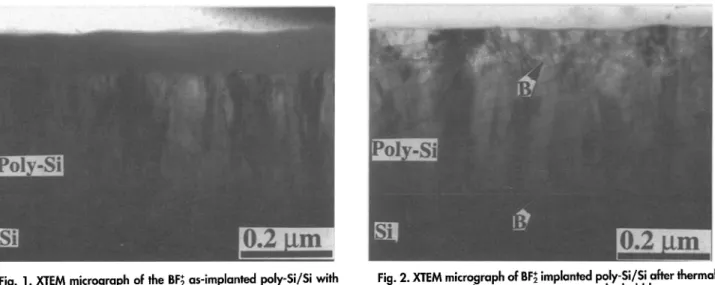
Fig. 1. XTEM micrograph of the BF,~ as-implant~ poly-Si/Si with Fig. 2. XTEM micrograph of BF~ implanted poly-Si/Si after thermal an energy of 80 keV anda dose of 6 • 10 Ts cm -2. annealing at 850~ far 30 min. B represents the bubbles.
2000 J. Electrochem. Soc., Vol. 142, No. 6, June 1995 9 The Electrochemical SecJety, Inc.
) unless CC License in place (see abstract).
ecsdl.org/site/terms_use
address. Redistribution subject to ECS terms of use (see
140.113.38.11
J. Electrochem. Soc.,
Vol. 142, No. 6, June 1995 9 The Electrochemical Society, Inc. 2001 the linear extrapolation of b o r o n profiles in the silicon to-w a r d the poly-Si/Si interface. I~'~7
Experimental
The substrates used in this experiment were n-type, (001)St wafers w i t h a resistivity of 0.5 to 2 ~ - c m . Prior to poly-Si film deposition, all wafers were dipped in a dilute HF solution to remove the surface native oxide followed by a deionized w a t e r rinse. Then, poly-Si films with a thick- ness of 350 nm were deposited in a low pressure chemical v a p o r deposition (LPCVD) system at 625~ w i t h Sill4 gas. The deposition pressure and deposition rate were about 180 to 220 reTort and 11 nm/min, respectively. During the LPCVD poly-Si deposition process, a native oxide was formed at the p o l y - S i / S i interface. All wafers were then implanted w i t h 80 keV BF~ to a dose of 6 • 101~ cm -2. After implantation, the wafers were annealed in the t e m p e r a t u r e range of 850 to 1100~ The structures of p o l y - S i / S i were examined by XTEM using a J E O L 200 CX microscope, op- erating at 200 keV. The boron and fluorine distribution pro- files was obtained with a Cameca IMS-4f ion microana- lyzer using O~ primary ion bombardment.
Results and Discussion
XTEM examination of poly-Si/Si sampIes.~As-im-
planted poIy-Si/Si samples.-- Figure
1 shows an XTE1V[ mi- crograph of a BF~-implanted p o l y - S i / S i sample. It can be seen that the poly-Si surface layer was completely amor- phized by the BF~ i m p l a n t a t i o n to a depth of about 100 nm from the surface.850~ annealed samples.--Figure
2 shows the XTEM mi- crograph of BF~-implanted p o l y - S i / S i after annealing at 850~ for 30 rain. It has been assumed that the fluorine is immobile w i t h i n the grains and that there is a strong emis- sion of fluorine from the grains into the grain boundaries. ~z However, the nature of fluorine in the poly-Si is not clearly understood owing to the complicated structure of poly-Si. As shown in Fig. 2, it can be seen that the amorphous layer was recrystallized into poly-Si after annealing. The recrys- tallized poly-Si films consists of residual defects. A high density of small fluorine bubbles was distributed in the recrystallized poly-Si films. The bubbles in the poly-Si films are distributed in a depth range of 60 to 110 nm be- n e a t h the poly-Si surface, which is n e a r the original a - S t / poly-Si surface. The distribution of bubbles is consistent with the observation of the presence of a fluorine peak in the recrystallized poly-Si films after annealing. It has been reported that the fluorine atoms tend to be gettered in the residual damage region. 1~ Fluorine bubbles are apparently formed from the accumulation of fluorine atoms and vacancies since the solid solubility of fluorine atoms is r a t h e r low. The fluorine bubbles were also observed in high dose BF~-implanted silicon after annealing at 1000 to 1100oc. 19,20 However, the formation of fluorine bubbles in the poly-Si film had not been reported previously. As shown in Fig. 2, the epitaxial alignment of poly-Si films did not occur in the 850~ annealed sample. It should be noted that a thin uniform layer of bubbles was found to develop at the original p o l y - S i / S i interface. The thickness of this bubble layer was estimated to be about 2.5 nm. The results are consistent w i t h the SIMS fluorine profile which shows a high concentration of fluorine atoms a c c u m u l a t e d at the p o l y - S i / S i interface after annealing. It has been reported that the fluorine atoms could react w i t h native oxide and Si to form Si oxyfluoride and Si f l u o r i d e J ~ Hence, the fluorine atoms accumulated at the po]y-Si/Si interface may react with interracial native oxide and form fluorine bubbles. As mentioned previously, the morphology of p o l y - S i / S i inter- face plays an i m p o r t a n t role in shaping the diffusion pro- files of doping impurity and the electrical properties of poly-Si emitter bipolar transistors. However, the formation of fluorine bubbles at the p o l y - S i / S i interface has not been reported previously.900~ annealed samples.--Figures
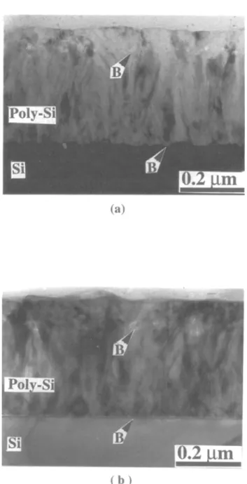
3a and b show XTEM micrographs of samples after annealing at 900~ for 30 andFig. 3. XTEM micrographs of BF~ implanted poly-Si/Si after thermal
annealing at 900~ for (a) 30 and (b) 60 min. B represents the
bubbles.
60 min, respectively. The bubbles are also distributed in the recrystallized po]y-Si films for both samples. The distribu- tion of bubbles in the p o l y - S i / S i is similar to that of 850~ annealed samples. The bubbles in the recrystallized poly-Si films were found to grow larger as compared with those in 850~ annealed samples. The sizes of bubbles were meas- ured to be 3 to 20 nm. The XTEM micrographs also reveal that the poly-Si films were epitaxi.ally aligned with silicon substrate in 900~ annealed samples. The m a x i m u m thick- ness of the epitaxially aligned poly-Si films were estimated to be 30 and 70 nm for 30 and 60 rain annealed samples, respectively. In contrast, a partial epitaxial regrowth of poly-Si on Si was observed in the p o l y - S i / S i with a thin Si-B layer as diffusion source after annealing at 1000~ for 30 min. ~ Moreover, the partial epitaxial regrowth of poly- Si on Si was observed in the u n i m p l a n t e d p o l y - S i / S i after annealing at 1100~ for 30 min. On the other hand, the epitaxial growth of poly-Si on Si was promoted by the presence of fluorine atoms at the p o l y - S i / S i interface. It should be noted that the fluorine bubbles were also ob- served at the original p o l y - S i / S i interface after epitaxial regrowth of poly-Si on St. The layer of bubbles located at the poly-Si and Si interface was disrupted to form bands of
bubbles during the epitaxial g r o w t h of poly-Si films. T h e thickness a n d length of b u b b l e b a n d s w e r e estimated to be 3.5 a n d 180 n m a n d 5 a n d 135 n m for 30 a n d 60 a n n e a l e d samples, respectively.
950~ annealed samples.--Figures
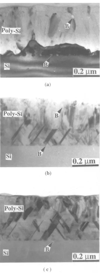
4a, b, a n d e s h o w the X T E M m i c r o g r a p h of samples after annealing at 950~ forFig. 4. XTEM micrographs of BF~ implanted poly-Si/Si after thermal
annealing at 950~ for (a) 15, (b) 30, and (c) 60 min. B represents the
bubbles.
15, 30, a n d 60 rain, respectively. It can be seen that m o s t of the bubbles in the recrystallized poly-Si films are dis- tributed in a depth range of 60 to ii0 n m b e n e a t h the poly- Si surface. T h e size of bubbles in the reerystallized poly-Si films w a s f o u n d to be larger as c o m p a r e d with those of 900~ annealed samples. T h e m a x i m u m size of bubbles in the poly-Si film in 950~ a n n e a l e d samples is as large as 40 n m . H o w e v e r , the density of bubbles in poly-Si film w a s decreased with annealing temperature a n d time. T h e X T E M m i c r o g r a p h s reveal that approximately 20, 30, a n d 45 % of poly-Si films w e r e epitaxially aligned with the sili- con substrate in samples annealed for 15, 30, a n d 60 min, respectively. T h e roughness of the epitaxial r e g r o w t h front of poly-Si film is increased with annealing time. In addi- tion, the fluorine bubbles w e r e also f o u n d to be present at the original poly-Si/Si interface in samples a n n e a l e d at 950~ T h e shape of bubbles at the original poly-Si/Si in- terface is similar to that in 900~ a n n e a l e d samples for annealing time less than 30 min. H o w e v e r , the length a n d w i d t h of b u b b l e b a n d s w e r e decreased a n d increased with annealing time, respectively. F o r a 60 rain a n n e a l e d sample, the shape of bubbles at the poly-Si/Si interface w e r e ob- served to be truncated octahedra with truncated faces par- allel to {i00}. It is interesting to note that one of the p r o m i - nent truncated faces of the bubbles is the original poly-Si/Si interface. T h e m a x i m u m size of the b u b b l e is as large as 24 n m .
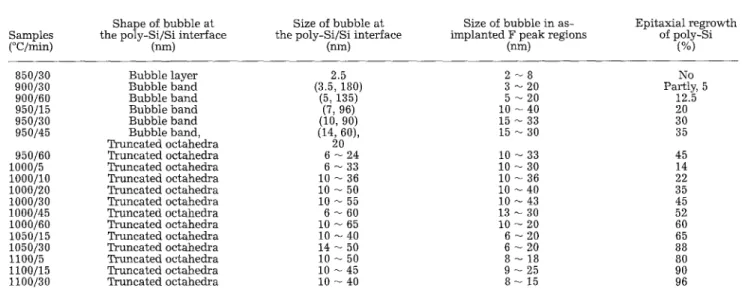
1000~ annealed samples.-- Figures
5a, b, a n d e s h o w the X T E M m i c r o g r a p h s of samples annealed at 1000~ for 5, 30, a n d 60 rain, respectively. B u b b l e s w e r e also observed in the recrystallized poly-Si films. H o w e v e r , the average size of bubbles in the poly-Si films in 1000~ a n n e a l e d s a m p l e w a s smaller than that of 950~ annealed samples. T h e sizes of b u b b l e w e r e estimated to be i0 to 30 n m . In addition, the density of bubbles in the poly-Si film is lower t h a n those in 350 to 950~ annealed sample. T h e X T E M m i c r o g r a p h s re- veal that approximately 15, 45, a n d 6 0 % of poly-Si films w e r e aligned epitaxially to silicon in s a m p l e annealed for 5, 30, a n d 60 min, respectively. T h e roughness of epitaxiil r e g r o w t h front w a s f o u n d to increase with annealing t e m - perature or time. Moreover, a high density of twins w a s observed to be distributed in the epitaxial r e g r o w t h films. T h e bubbles w e r e also observed at the poly-Si/Si interfaces in all three samples. T h e shape of bubbles at the poly-Si/Si interface w e r e observed to be truncated octahedra with truncated faces parallel to {i00}. O n e of truncated faces of bubbles correspond to the original poly-Si/Si interface. It w a s also f o u n d that the average size a n d the density of bubbles at the original poly-Si/Si interface w e r e increased a n d decreased with annealing time, respectively. T h e m a x i - m u m size of bubbles .at the poly-Si/Si interface could be as large as 65 n m (1000~ 60 min).1100~ annealed samples.--Figures
6a, b, a n d c s h o w the X T E M m i c r o g r a p h s of B F ~ - i m p l a n t e d poly-Si/Si after an- nealing at II00~ for 5, 15, a n d 30 min, respectively. It is seen that m o s t of poly-Si films are epitaxially aligned with the silicon substrate for all three samples. A high density of twins w e r e also observed to be distributed in the epitaxial r e g r o w t h poly-Si films. T w o groups of fluorine bubbles w e r e observed in epitaxial r e g r o w t h films. T h e depth dis- tribution of bubbles is the s a m e as those in the samples annealed at 850 to 1000~ S o m e of the bubbles w e r e ob- served in depths ranging f r o m 50 to i00 n m b e n e a t h the surface. H o w e v e r , the size a n d the density of bubbles in the as-implanted p e a k regions are m u c h smaller than those in 900 to 1000~ annealed samples. The size of bubble w a s estimated to be 5 to 25 nm. Another group of bubbles was distributed at the original poly-Si/Si interface. The shape of bubbles at the original poly-Si/Si interface is the s a m e as that in the 1000~ annealed samples. It w a s also found that the n u m b e r of bubbles at the poly-Si/Si interface de- creased with increasing annealing time; however, the size of the bubbles did not increase with annealing time. This implies that some of fluorine atoms outdiffused from the poly-Si/Si interface for II00~ annealed sample. The re-) unless CC License in place (see abstract).
ecsdl.org/site/terms_use
address. Redistribution subject to ECS terms of use (see
140.113.38.11
J. Electrochem. Soc.,
Vol. 142, No. 6, June 1995 9 The Electrochemical Society, Inc. 2003 the substrate with annealing temperatures and times are summarized in Table I.SIMS fluorine profile.--Figure
7 shows the SIMS fluo-rine distribution profiles of BF~ a s - i m p l a n t e d poly-Si/Si and samples after thermal a n n e a l i n g in the temperature range of 850 to ll00~ for 30 min. The as-implanted fluo- rine peak is present at a depth of 75 n m beneath the poly-Si surface. After thermal annealing, the fluorine atoms are redistributed significantly a n d double fluorine peaks are
Fig. 5. XTEM micrograph of BF~ implanted poly-Si/Si after thermal
annealing at 1000~ far (a) 10, (b) 30, and(c) 60 min. B represents
the bubbles.
sults are consistent w i t h the S I M S fluorine profile w h i c h s h o w s the fluorine concentrations in the as-implanted p e a k region a n d at the poly-Si/Si interface are considerably de- creased in 1 1 0 0 ~ a n n e a l e d sample.
Finally, the variations of the s h a p e a n d the size of the fluorine b u b b l e s a n d the epitaxial r e g r o w t h of poly-Si o n
Fig. 6. XTEM micrographs of BF~ implanted poly-Si/Si after thermal
annealing at 1100~ for (a) 5, (b) 15, and (c) 30 min. B represents the
bubbles.
Table I. The variations of the shape and the size of fluorine bubble and the epitaxial regrowth of poly-Si
with annealing temperatures and times.
S h a p e of bubble at Size of bubble at Size of bubble in as- Epitaxial regrowth S a m p l e s the poly-Si/Si interface the poly-Si/Si interface implanted F peak regions of poly-Si
(~ (nm) (nm) (rim) ( % )
850/30 Bubble layer 2.5 2 ~ 8 No
900/30 Bubble band (3.5, 180) 3 ~ 20 Partly, 5
900/60 Bubble band (5, 135) 5 ~ 20 12.5 950/15 Bubble band (7, 96) 10 - 40 20 950/30 Bubble band (10, 90) 15 ~ 33 30 950/45 B u b b l e band, (14, 60), 15 ~ 30 35 Truncated octahedra 20 950/60 Truncated octahedra 6 ~ 24 i0 -~ 33 45 1000/5 Truncated octahedra 6 ~ 33 I0 -- 30 14
i000/I0 Truncated oetahedra I0 ~ 36 I0 - 36 22
1000/20 Truncated oetahedra I0 - 50 i0 ~ 40 35 1000/30 Truncated octahedra 10 ~ 55 10 ~ 43 45 1000/45 Truncated octahedra 6 ~ 60 13 ~ 30 52 1000/60 Truncated octahedra t0 ~ 65 10 ~ 20 60 1050/15 Truncated octahedra 10 ~ 40 6 ~ 20 65 1050/30 Truncated octahedra 14 ~ 50 6 ~ 20 88 1100/5 Truncated octahedra 10 ~ 50 8 ~ 18 80 1100/15 Truncated octahedra 10 -~ 45 9 ~ 25 90 1100/30 Truncated octahedra 10 ~ 40 8 ~ 15 96
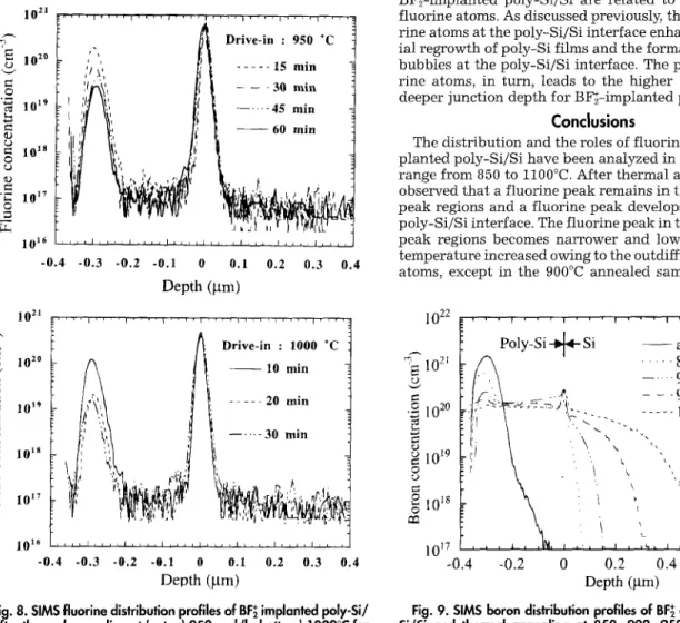
observed in the SIMS fluorine profiles. The locations of fluorine peaks are consistent w i t h the distribution of fluo- rine bubbles. A fluorine peak remains after t h e r m a l an- nealing at the a s - i m p l a n t e d fluorine peak regions. The fluorine p e a k becomes n a r r o w e r and w e a k e r as the anneal- ing t e m p e r a t u r e increases, except for the 900~ annealed sample. It is a t t r i b u t e d to the outdiffusion of fluorine atoms and the f o r m a t i o n of fluorine bubbles during t h e r m a l an- nealing. For the 900~ annealed sample, the fluorine profile becomes n a r r o w e r as compared w i t h the a s - i m p l a n t e d pro- file; however, the fluorine p e a k concentration is greater t h a n t h a t of the a s - i m p l a n t e d fluorine p e a k concentration. The p h e n o m e n o n was also observed in heavily BF~-im- p l a n t e d silicon after annealing at 900~ 18 It is considered to be the gettering of fluorine atoms by the residual defects induced by the implantation. The gettering of fluorine atoms is relatively strong at this temperature. This is con- sistent w i t h the XTEM observation, as shown in Fig. 3, t h a t fluorine bubbles grew at this temperature. In addition, a fluorine p e a k was found to develop at the original p o l y - S i / Si interface after t h e r m a l annealing. As m e n t i o n e d previ- ously, a native oxide was formed at the p o l y - S i / S i interface during the LPCVD processes. It is well k n o w n that the ox- ide layer acts as a favorable site for the gettering of fluorine atoms. 2~ Moreover, it has been reported that the diffusion of fluorine in the p o l y - S i films is d o m i n a t e d by the grain b o u n d a r y diffusion. 12 Therefore, the fluorine p e a k at the p o l y - S i / S i interface arises from the diffusion of fluorine atoms along the poly-Si grain b o u n d a r y and accumulates at the p o l y - S i / S i interface during t h e r m a l annealing. It should be noted t h a t the fluorine peak concentration at the p o l y - S i / S i interface for 900~ annealed sample is also greater t h a n those in other samples. However, the fluorine profiles at the p o l y - S i / S i interface are almost the same for 850, 950, and 1000~ samples. The reasons for this phe- n o m e n o n are possibly the same as previously discussed. In samples annealed at 1100~ b o t h fluorine peaks are obvi- ously decreased since most of the fluorine atoms diffused out. The results are consistent w i t h those shown in Fig. 6 w h i c h indicates that the density and the size of bubbles in l l 0 0 ~ samples are m u c h smaller t h a n those in 900 to 1000~ annealed samples. Between two fluorine peaks (the region - 0 . 2 to 0.1 btm), the fluorine concentrations de- creased w i t h increasing annealing temperatures. It is con- sidered to be the reduction of the grain b o u n d a r y area be- cause of the increasing of poly-Si grain size and the epitaxial r e g r o w t h of poly-Si films. Figures 8a and b show the SIMS fluorine profiles as a function of annealing time for 950 and 1000~ annealed samples, respectively. At the a s - i m p l a n t e d fluorine p e a k region, the fluorine peaks be- come slightly n a r r o w e r and lower as the annealing time increases. It is also considered to be due to the outdiffusion
of fluorine atoms. However, the fluorine profiles at the p o l y - S i / S i interface are almost the same for different an- nealing times at t e m p e r a t u r e s 900 to 1000~ The results indicate that the pileup of fluorine atoms at the p o l y - S i / S i interface is rapidly saturated. Moreover, the fluorine con- centration is low in the region between two fluorine peaks. This indicates that the solid solubility of fluorine atoms in the poly-Si is r a t h e r low.
Boron diffusion profiles.--The
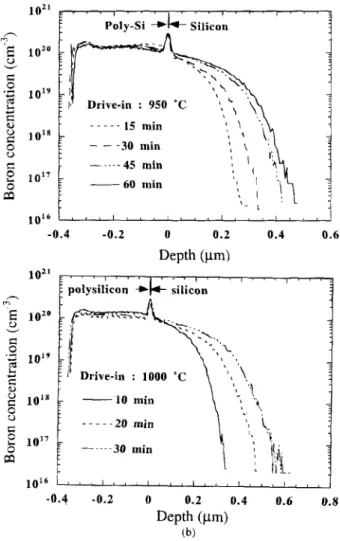
diffusion behaviors ofboron in the BF~-implanted p o l y - S i / S i has been widely in- vestigated by several researchers. However, the effects of fluorine on boron diffusion are not clearly understood. Fig- ure 9 shows the boron profiles of a s - i m p l a n t e d p o l y - S i / S i and samples after annealing in the t e m p e r a t u r e range of 850 to 1000~ for 30 rain. It can be seen t h a t a boron p e a k remains near the poly-Si surface for 850~ annealed sam- ples. The boron peaks gradually disappeared as the anneal- ing t e m p e r a t u r e increased. It has been reported that the diffusion of boron in the poly-Si is strongly affected by the solid solubility l i m i t Y The boron diffusivity is drastically reduced in the poly-Si where the boron concentration ex- ceeds the solid solubility limit. The formation of boron pre- cipitates w h i c h reduces the boron diffusivity has been sug- gested for high dose BF~-implanted samples. ~ In the present experiment, the XTEM micrographs reveal that t h e fluo- rine bubbles are distributed in the recrystallized poly-Si films after annealing. Moreover, the peak portions of F pro- files are close to those of the B profiles. It has been reported t h a t the dopant atoms are prone to be gettered by the resid- ual defects. This indicated t h a t the boron atoms could be gettered by the fluorine bubbles in the recrystallized poly- Si films. 23 In addition, it is interesting to n o t e that a s m a l l b o r o n p e a k is p r e s e n t at the poly-Si/Si interface in all a n - n e a l e d s a m p l e s . T h e b o r o n p e a k c o n c e n t r a t i o n s w e r e esti- m a t e d to b e 1.7 • 102~ 2.8 • 102~ 2.6 • 102~ a n d 2.7 • 1020 for 850, 900, 950, a n d 1 0 0 0 ~ a n n e a l e d s a m p l e , respectively. M o r e o v e r , as s h o w n in Fig. 1 0 a a n d b, it w a s f o u n d that the b o r o n p e a k c o n c e n t r a t i o n are i n d e p e n d e n t of a n n e a l i n g t i m e for 9 5 0 a n d 1 0 0 0 ~ a n n e a l e d s a m p l e s . T h e results are consistent w i t h the fluorine profiles s h o w n in Fig. 7 a n d 8. A s s h o w n previously, the fluorine b u b b l e s w e r e f o u n d to b e p r e s e n t at the poly-Si/Si interface in all a n n e a l e d s a m p l e s . Therefore, the b o r o n p e a k at the poly-Si/Si interface is c o n s i d e r e d to result f r o m the gettering of b o r o n a t o m s b y the fluorine b u b b l e s at the original poly-Si/Si interface.
It is we]] k n o w n that the segregation of the fluorine a t o m s in thin gate o x i d e e n h a n c e s the p e n e t r a t i o n of b o r o n a t o m s . A s s h o w n in Fig. 7, it c a n b e s e e n that a large n u m - b e r of fluorine a t o m s piled u p at the original poly-Si/Si interface after annealing. In a p r e v i o u s study, it w a s d e m o n s t r a t e d that the b o r o n profiles of B F ~ - i m p l a n t e d
) unless CC License in place (see abstract).
ecsdl.org/site/terms_use
address. Redistribution subject to ECS terms of use (see
140.113.38.11
J. Electrochem. Soc.,
Vol. 142, No. 6, June 1995 9 The Electrochemical Society, Inc. 2005 1 0 2 2 I 1 0 21 L)0
1 0 2 0 * v,,,,,~=
10~9
=
~
101~
=
O
1017
1016
I ,- 0 . 4
, , , , i , , , , I , , , , i , , , , i , , , , i , , , r l , , , , I , , , ,D r i v e - i n t i m e : 3 0 m i n
:/
- -
a s - i m p l a n t e d
9 ~ :,' /
,'"\ \
,t: t.':
. . .
900 *C
r,
*
" i- 0 . 3
- 0 . 2
- 0 . 1
0
0.1
0 . 2
0 . 3
0 . 4
D e p t h
( tm)
Fig. 7. SIMS fluorine distribu-
tion profiles of BF~ as-implanted
poly-Si/Si and samples after an-
nealing at 850, 900, 950, 1000,
and 1100~ for 30 min.
poly-Si source in the silicon substrates are m o r e sensitive to the thermal b u d g e t than that of the Si-B layer source. ~ It is attributed to the larger surface concentration, C~, for
= O = 2 10 zi 102o O 1019 = 10 is 0 r o 9 ~ 1017 C~ 1016 . . . . i ~ , , , i , , , , , . . . . ,'/F, i i . . . . L . . . . i . . . . I . . . . Drive-in : 950 *C . . . 15 r a i n - -- - 30 r a i n . . . 45 r a i n 60 r a i n 10 zl 1020 l 0 t s 1 0 1 7 1016 - 0 . 4 - 0 . 3 - 0 . 2 - 0 . 1 0 0.1 0 . 2 0 . 3 0 . 4 D e p t h (~tm) . . . . i . . . . i . . . . i , , , Drive-in : 1000 *C - - 10 min . . . 20 rain . . . 30 rain :\ ': ' , I / ' , . ,1', - 0 . 4 - 0 . 3 - 0 . 2 -0.1 0 0.1 0 . 2 0 . 3 0 . 4 D e p t h (gin)
Fig. 8. SIMS fluorine distribution profiles of BF~ implanted poly-Si/
Si after thermal
a n n e a l i n g a t {a, top) 9 5 0 a n d (b, b o f f o m ) 1 0 0 0 ~ f a r10 to 60 min.
B F ~ - i m p l a n t e d poly-Si/Si. A s s h o w n in Fig. 9, it can be seen that the C, values increased with temperature. Moreover, the Cs values are i n d e p e n d e n t of annealing time as seen f r o m Fig. 10a a n d b. Therefore, the higher C, values for B F ~ - i m p l a n t e d poly-Si/Si are related to the presence of fluorine atoms. A s discussed previously, the pileup of fluo- rine a t o m s at the poly-Si/Si interface e n h a n c e s the epitax- ial r e g r o w t h of poly-Si films a n d the formation of fluorine bubbles at the poly-Si/Si interface. T h e presence of fluo- rine atoms, in turn, leads to the higher C, values a n d a deeper junction depth for B F ~ - i m p l a n t e d poly-Si source.
Conclusions
The distribution and the roles of fluorine in the BF~-im- p l a n t e d p o l y - S i / S i have been analyzed in the t e m p e r a t u r e range from 850 to 1100~ After t h e r m a l annealing, it was observed t h a t a fluorine p e a k remains in the a s - i m p l a n t e d p e a k regions and a fluorine p e a k develops at the original p o l y - S i / S i interface. The fluorine p e a k in the a s - i m p l a n t e d p e a k regions becomes n a r r o w e r and lower as annealing t e m p e r a t u r e increased owing to the outdiffusion of fluorine atoms, except in the 900~ annealed sample. This is ex-
10 22 m '~ 10 21 8 .~ 10 20 g 10~9 2 10~8 1017 ' ' ' I ' ' ' I ' ' ' I ' ' ' I ' ' ' 1 ' ' ' Poly-Si + Si as-implanted ...
850 ~
1' ..\ . . . . 900 ~ I s ~, - - --~', - - -950 ~, t i - " T "
- . . . . looo ~
...
.~,,
. 2, ,\, ,'i! . . . -0., -0.2 0 0.2 0.4 0.6 0.8 Depth (gm)Fig. 9. SIMS boron distribution profiles of BF~ as-implanted poly-
Si/Si and thermal annealing at 850, 900, 950, and 1000~ for
30 min.
1021 ' ' ' i 9 ' ' | , , . , . . 1 q , , Poly-Si -~l'q-- Silicon '~ 102o , -
. . . .
9 ~ 1 0 1 9 c ~ r 1 0 I S . . . 1 5 m i n ', ' \ ~ e - 1 0 1 7 . . . 45rain 'i " '%~ 1 0 1 6 , l t i I r J i i 5 I I i I I , I -o.4 - o n o 0.2 0.4 0 . 6Depth
(gm)
10 ~ polysilicon - ~ - silicon . ~ 10 ~~ ~-. ~'~, 10 Is ', "1 10'7 ~ ', :i 1 0 1 6 , , I , , J I J * i I I i , i I i i I -0.4 -0.2 0 0.2 0.4 0.6 0.8Depth (gin)
it,)
Fig. 10. SIMS boron distribution profiles of BF~ implanted poly-Si/ Si after thermal annealing at (a, top) 950 and (b, bottom) 1000~ for 15 to 60 min.
p]ained b y the effects of the outdiffusion of fluorine a t o m s a n d the formation of fluorine bubbles. T h e pileup of fluo- rine a t o m s at the poly-Si/Si has the effects of e n h a n c i n g epitaxial r e g r o w t h of poly-Si films a n d the formation of fluorine bubbles. T h e formation of fluorine bubbles re- sulted f r o m the a c c u m u l a t i o n of fluorine atoms. It w a s also f o u n d thai the shapes, the size, a n d the density of bubbles at the poly-Si/Si interface are related to annealing temper- ature a n d time. T h e a p p e a r a n c e of the b o r o n p e a k at the original po]y-Si/Si interface is attributed to be the getter- ing of b o r o n a t o m s b y the fluorine bubbles. In addition, the presence of fluorine atoms leads to the higher
Cs
values, and the boron profiles in the silicon substrate are sensitive to thermal budget. The results demonstrated that the pres- ence of fluorine atoms plays an i m p o r t a n t role i n the a n - n e a l i n g behaviors of B F ; - i m p l a n t e d poly-Si/Si systems.Acknowledgment
T h e authors are grateful to C. C, W a n g for S I M S m e a s - urement. This w o r k w a s supported b y the National Science Council of the Republic of C h i n a u n d e r Contract No. N S C 84-2215-E009-023.
Manuscript submitted Oct. 7, 1994; revised m a n u s c r i p t received Feb. 16, 1995.
National Chiao Tung University assisted in meeting the
publication costs of this article.
R E F E R E N C E S
I. M . H. E I - D i w a n y , M . P. Brassington, P. Tuntasood, R. R. R a z o u k , a n d M . W. Poulyer, I E E E Trans. Electron
Devices,
ED-35, 1556 (1988).2. G. L. Patton, J. C. Bravman, a n d J. D. Plummer,
ibid.,
ED-33, 1754 (1986).3. T. Kamins,
PolycrystaIline Silicon for Integrated Cir-
cuit Applications,
Kluwer Academic, Boston (1988).4. Polysilicon Emitter Bipolar Transistors,
A. K. Kapoora n d D. J. Roulston, Editors, IEEE Press, New York (1989).
5. J.M.C. Stork, M. Arienzo, a n d C. Y. Wong,
IEEE Trans.
Electron Devices,
ED-32, 1766 (1985).6. K. L. Mclaughlin, M. A. Taylor, a n d G. Sweeney,
AppI.
Phys. Lett.,
47, 992 (1985).7. K. Park, S. Batra, S. Banerjee, G. Lux, a n d R. M a n u - kondo,
This Journal,
138, 545 (1991).8. I. R. C. Post a n d P. Ashburn,
IEEE Trans. Electron
Devices,
ED-38, 2442 (1991).9. P.-F. Lu, J. D. Warnock, J. D. Cressler, K. A. Jenkins, and K.-Y. Toh,
ibid.,
ED-38, 1410 (1991).10. S. L. Wu, C. L. Lee, T. F. Let, and H.-C. Chang,
ibid.,
ED-40, 1797 (1992).11. J. J. Sung a n d C.-Y. Lu,
ibid.,
ED-37, 2312 (1990). 12. H.-H. Tseng, M. Orlowski, R J. Tobin, a n d R. L. Hance,IEEE Trans. Electron Device Lett.,
EDL-13, 14 (1992).13. G, D. Williams a n d R Ashburn,
.7. Appl. Phys.,
72, 3169 (1992).14. S. L. Wu, C. L. Lee, T. E Let, C. F. Chen, L. J. Chen, K. Z. Ho, a n d Y. C. Ling,
IEEE Trans. Electron Device
Lett.,
EDL-15, 120 (1994).15. T. R Chen, T. E Let, H. C. Lin, a n d C. Y. Chang,
This
Journal,
142, 532 (1995).16. H. Schaber, R. V. Criegen, a n d I. Weitiel,
J. Appl. Phys.,
58, 4036 (1985).17. B. Garben, W. A. Orr-Arienzo, a n d R. L. Lever,
This
Journal,
133, 2152 (1986).18. M.Y. Tsai, D. S. Day, B. G. Streetman, R Williams, a n d C. A. Evans,
J. AppI. Phys.,
50, 188 (1979).19. C. W. Nieh a n d L. J. Chen,
Appl. Phys. Lett.,
48, 1528 (1986).20. C. W. Nieh a n d L. J. Chen,
J. Appl. Phys.,
60, 3114(1986).
21. S.-P. Jeng, T.-E Ma, R. Canteri, M. Anderle, a n d G . W. Rubloff,
Appl. Phys. Lett.,
61, 1310 (1992).22. B. Yu, E. Arai, Y. Nishioka, Y. Ohji, S. Iwata, and T. P. Ma,
ibid.,
56, 1430 (1990).23. R.-D. Chang, T.-E Chen, a n d J. S. Fu,
SSDM,
401 (1992).) unless CC License in place (see abstract).
ecsdl.org/site/terms_use
address. Redistribution subject to ECS terms of use (see
140.113.38.11