Improved efficiency for nanopillar array of c-Si photovoltaic by
down-conversion and anti-reflection of quantum dots
Chien-Chung Lin
a*, Hsin-Chu Chen
b, Hau-Vei Han
b, Yu-Lin Tsai
b, Chia-Hua Chang
b, Min-An Tsai
c,
Hao-Chung Kuo
b, and Peichen Yu
ba
Institute of Photonic System, National Chiao Tung University, Tainan 711, Taiwan, R. O. C.
bDepartment of Photonics and Institute of Electro-Optical Engineering, National Chiao Tung
University, Hsinchu 30010, Taiwan
c
Department of Electro-physics, National Chiao Tung University, Hsinchu 30010, Taiwan, R. O. C.
E-Mail: [email protected]
ABSTRACT
Improvement of efficiency for crystalline silicon (c-Si) with nanopillar arrays (NPAs) solar cell was demonstrated by deployment of CdS quantum dots (QDs). The NPAs was fabricated by colloidal lithography of self-assembled polystyrene (PS) nanospheres with a 600 nm in size and reactive-ion etching techniques, and then a colloidal CdS QDs with a concentration of 5 mg/mL was spun on the surface of c-Si with NPAs solar cell. Under a simulated one-sun condition, the device with CdS QDs shows a 33% improvement of power conversion efficiency, compared with the one without QDs. Additionally, we also found that the device with CdS QDs shows a 32% reduction in electrical resistance, compared with the one without QDs solar cell, under an ultraviolet (UV) light of 355nm illumination. This reduced electrical resistance can directly contribute to our fill-factor (FF) enhancement. For further investigation, the excitation spectrum of photoluminescence (PL), absorbance spectrum, current-voltage (I-V) characteristics, reflectance and external quantum efficiency (EQE) of the device were measured and analyzed. Based on the spectral response and optical measurement, we believe that CdS QDs not only have the capability for photon down-conversion in ultraviolet region, but also provide extra antireflection capability.
Keywords: Solar cell, Photovoltaic, Down-conversion, Antireflection, Nanopillars, Quantum dots
1. INTRODUCTION
Single crystalline and amorphous silicon solar cells have been important research topics for decades due to their environmental-friendly, stable characteristics, good power conversion efficiency, and mature semiconductor industrial supports. However, there are still many problems in Si-based solar cells needed to be resolved in order to achieve high efficiency. Especially, the high contrast of refractive index of silicon causes a high Fresnel reflectivity at silicon-air interfaces and severely limits the performance of Si-based optoelectronic devices [1]. In order to reduce Fresnel reflection in the solar cells, effective antireflective coatings (ARCs) have been developed [2]. The general single layer or multilayer ARC is composed of a quarter wavelength stack of dielectrics with different refractive indices, such as silicon nitride or silicon dioxide [3]. However, these complicated dielectric layers need expensive equipment with high-vacuum chamber, and precise layer thickness control. All of these measures could put the overall cost of solar cells unbearable. Consequently, some research laboratories have developed sub-wavelength structures to eliminate such kind of reflection and improved cell efficiency, such as nanowire or nanotips [4], and it is more stable and enduring than surface coatings since only one material is involved. The basic purpose of this technique is to introduce an effective intermediate refractive index layer between air and the substrate material by the spatial profile of nanostructures [5]. Ideally, a tapered profile with sharp tips can provide this feature in terms of refractive index gradient. However, such nanostructures are not preferred in solar cell due to considerable surface recombination. Besides using ARC to pass more lights into the solar cell, we also have to fully utilize the available solar energy as efficient as possible. However, under the ultraviolet (UV) and near-UV illumination, most of photons are absorbed near the surface of the cell and the collection probability of the generated electron-hole pairs near surface of the Si solar cells is very poor, so the short-wavelength part of the solar spectrum cannot be used completely by Si solar cells with ordinary design.
Physics, Simulation, and Photonic Engineering of Photovoltaic Devices,
Edited by Alexandre Freundlich, Jean-Francois F. Guillemoles, Proc. of SPIE Vol. 8256, 825609 © 2012 SPIE · CCC code: 0277-786X/12/$18 · doi: 10.1117/12.908514
Proc. of SPIE Vol. 8256 825609-1
In this work, we investigate a method by combining the c-Si Nano Pillar Arrays (NPAs) solar cell with CdS QDs layers together, which improves the power conversion efficiency by nearly 33%, compared with the c-Si NPA solar cell without CdS QDs layers. The enhancement was confirmed by the photovoltaic I–V characteristics and the quantum efficiency measurement. It is found that with CdS QDs layers solar cell can improve cell efficiency, especially in the short-circuit current and fill-factor. Based on the spectral response and optical measurement, we demonstrate that CdS QDs layers not only have the capability for photon down-conversion in ultraviolet region but also provide extra antireflection capability and current conductivity for the improvement of Si-based solar cell efficiency.
2. INTRODUCTION
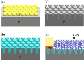
In this experiment, we use colloidal lithography method [6] to fabricate c-Si NPA solar cell. As the processes are schematically illustrated in Fig. 1 (a), first, a monolayer of self-assembled 600 nm polystyrene (PS) nanospheres with a plurality of 10 wt% was spin-cast onto the surface of a p-type c-Si substrate. A nearly-close-packed 600 nm PS nanospheres monolayer was then obtained on the c-Si substrate through tuning the degree of hydrophilicity, spinning speed, and the mixture concentration. After steady air-drying for 15 minute, the sample shown in Fig. 1 (a) was etched by an inductively coupled plasma reactive ion etching (ICP-RIE) system, where a reactive gas Cl2 was introduced to
bombard the nanospheres and the underlying c-Si substrate simultaneously with an RF power of 1000 W, a bias power of 150 W, under a 5 mTorr pressure at 60°C for 140 seconds. The sample was brushed and dipped into a pure acetone solution for 5 minutes at room temperature, which resulted in nearly close-packed NPA on the c-Si surface, as shown in Fig. 1 (b). Next, the NPA substrate was doped using phosphorus oxychloride (POCl3) as the diffusion source to form an
n-type layer, about 200 nm deep from the surface. After the removal of the phosphosilicate glass (PSG) layer from the substrate surface with diluted hydrofluoric (HF) acid, as shown in Fig. 1 (c), an 80-nm-thick silicon nitride (SiNx) layer
was deposited to passivate the surface by using plasma-enhanced chemical vapor deposition (PECVD). Then the front and back metal contacts were screen-printed and a co-firing in a furnace system at 850°C. Finally, a colloidal CdS QDs with a concentration of 5 mg/mL was spun on the surface of c-Si NPA solar cell, as shown in Fig. 1 (d). For comparison, the one without the CdS QDs layers was also fabricated simultaneously as the reference.
Fig. 1. The schematic fabrication flow for c-Si nanopillar arrays (NPA) solar cell with CdS quantum dots (QDs) layers: (a) spin-cast of nearly-close-packed polystyrene nanospheres monolayer, (b) resulting NPA after dry etching, (c) diffusion of an N-type layer. (d) SiNx deposition and screen printing of the front and back electrodes, and then spin CdS QDs layers on the cell.
In the Fig. 2 (a), we show the scanning electron microscopic (SEM) image of c-Si NPA in which the periodic pattern is accurately transferred onto the Si substrate after RIE. The height and shape of NPA can be controlled by varying the etching duration and our process control shaped the height of the NPA to be around 550 nm. In order to inspect experimental result of c-Si NPA solar cell after the addition of CdS QDs layers, the transmission electron microscopy (TEM) samples were also prepared using focus ion beam (FIB) techniques. The TEM image was taken near the edge of metal contact and the thickness of the CdS layer is ~6 nm, as shown in Fig. 2 (b). The element of CdS QDs layers was analyzed by Energy Dispersive Spectrometer (EDS), as also shown in (inserts of under corner) the image. Therefore, we can confirm the existence of Cd and S elements on the cell.
Proc. of SPIE Vol. 8256 825609-2
Fig. 2. The schematic fabrication flow for c-Si nanopillar arrays (NPA) solar cell with CdS quantum dots (QDs) layers: (a) spin-cast of nearly-close-packed polystyrene nanospheres monolayer, (b) resulting NPA after dry etching, (c) diffusion of an N-type layer. (d) SiNx deposition and screen printing of the front and back electrodes, and then spin CdS QDs layers on the cell.
3. INTRODUCTION
Fig. 3 (a) shows the diagram of CdS QDs absorption and emission spectra. The photoluminescence spectrum shows a peak at 430 nm, and 550 nm excited by photons with 365 nm or shorter wavelengths. The broad peak is attributed to the trap-states emission of CdS QDs [7]. The absorbance spectrum gradually increases from 375nm towards 330 nm. It is obvious that CdS QDs exhibit photon down-conversion from ultraviolet to visible light (from ~330 to 550 nm). This converted light can provide more photons to be harvested in c-Si NPA solar cell. Fig. 3 (b) shows reflectance spectra by an integrating sphere at the normal incidence of light. The c-Si NPA with CdS QDs layers exhibited superior antireflective properties for the wavelength range of interest, especially in the range of wavelength from 450 nm to 1100 nm, compared with the cell without CdS QDs layers. It is found that the CdS QDs layers provide a better antireflection layer for light harvest.
Fig. 3. (a) UV-Vis absorbance (red) and photoluminescence (blue) spectra of CdS QDs measure in toluene. The PLE spectrum was taken at the maximum of PL intensity (~430 nm). For the PL spectrum, the sample was excited by a light beam with 365 nm. (b) The measured reflectance spectra for cells with c-Si nanopillar arrays (NPA) with and without CdS quantum dots (QDs) layers.
4. INTRODUCTION
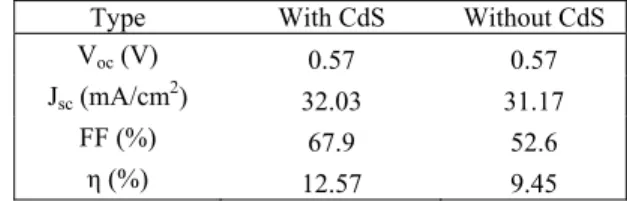
4.1 Photovoltaic characterizationThe photovoltaic I–V characteristics were measured under air mass 1.5 global illumination and room temperature conditions by a class-A solar simulator with a xenon flash tube of IEC 904–9 standard. Fig. 4 shows the photovoltaic I–V characteristics of the c-Si NPA solar cell with and without CdS QDs layers. The device characteristics were summarized
Proc. of SPIE Vol. 8256 825609-3
in Table 1. The short-circuit current density (Jsc) of the c-Si NPA solar cell with CdS QDs layers can reach 32.03
mA/cm2, meanwhile the power conversion efficiency is increased from 9.45% to 12.57%, corresponding to a 33%
enhancement compared with the reference. It is also noticeable that open-circuit voltage (Voc) shows negligible change.
Additionally, the fill-factor (FF) is improved, which is an indicator of better series resistance of the device. To further investigate the reason behind this FF improvement, we measure the resistance between individual metal contacts with and without CdS QDs layers under a UV light irradiation of 355nm wavelength. The change brought by the QD coating is significant: the resistances dropped from 43.4 Ω to 29.3 Ω. This 32% reduction in electrical resistance should be the direct cause of our FF improvement. From the photovoltaic IV measurement, we can see the enhancement of the solar cell with QDs layers.
Fig. 4. Photovoltaic I–V characteristics of the c-Si nanopillar arrays (NPA) solar cell with and without CdS quantum dots (QDs) layers.
Table 1. Current-Voltage Characteristics of c-Si NPA Solar Cells with and without CdS QDs layers. Type With CdS Without CdS
Voc (V) 0.57 0.57
Jsc (mA/cm2) 32.03 31.17
FF (%) 67.9 52.6
η (%) 12.57 9.45
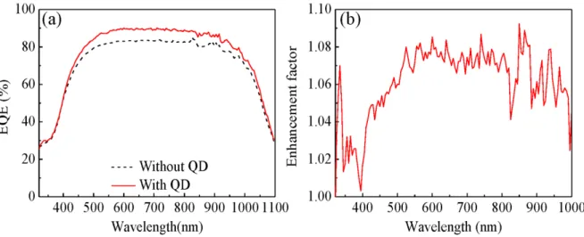
However, it is still unclear whether this improvement is from down-conversion photons or from other factors. To understand more thoroughly on the interaction of QDs with photons, we measured the spectral response of the external quantum efficiency (EQE). Fig. 5 (a) shows the EQE of the c-Si NPA solar cell with and without CdS QDs layers, and Fig. 5 (b) shows the EQE enhancement factor of the devices with CdS QDs layers, compared with reference cell. The cell with CdS QDs layers shows an enhanced EQE in the range from 320nm to 1100nm. According to Fig. 3 (a), the absorbance spectrum gradually increases from 375nm towards 330 nm, and this agrees with the peak position of enhancement of EQE at 335nm, as shown in Fig. 5 (b). The overall shape of EQE enhancement resembles the absorption curves in Fig. 3, and we believe this is a strong indication of QD absorption and down-conversion process. Most of electron–hole pairs generated in this UV regime are located near surface of device, and the surface defects consume most of the photo-generated carriers, which lead to inferior cell efficiency in UV wavelength range. Therefore, the addition of CdS QDs layers on the c-Si NPA solar cell can produce photon down-conversion effect, in which QD-originated photons with visible wavelengths can be absorbed in the depletion region, and the power conversion efficiency is improved. On the other hand, when the incident photons’ wavelength is longer than 425nm, the QDs layer is served more like an AR coating, which can also enhance the light harvesting.
Proc. of SPIE Vol. 8256 825609-4
Fig. 5. (a) Measurement of External quantum efficiency of the fabricated c-Si nanopillar arrays (NPA) solar cell with and without CdS QDs layers. (b) Peak (at ~335 nm wavelengths) of short-wavelength enhancement of in EQE indicates photon down-conversion.
4.2 Calculation
To characterize the contribution of down-conversion effect in the short-wavelength range, we further calculated the effective current due to the down-conversion of CdS QDs layers on the surface of the c-Si NPA solar cell. These photo-generated carriers can be observed directly from the short-circuit currents of a solar cell. The short-circuit density without and with CdS QDs, Jsc and Jsc,QDs can be calculated as follows:
1100 1.5 320
( )
( )
nm sc nm AM Ge
J
EQE
I
d
hc
λ
λ
λ λ
=
×
∫
×
×
(1)[
]
400 , 320 1.5 400 1.5 320 1100 1.5 400(
1
( )
( )
( )
( )
( )
( )
( )
( )
)
nm sc QDs nm AM G nm AM G nm nm AM G nme
J
A
EQE
I
d
hc
A
EQE
QY I
d
EQE
I
d
λ
λ
λ
λ λ
λ λ
λ
λ λ
λ
λ
λ λ
=
×
−
× ×
×
+
× ×
×
×
+
×
×
∫
∫
∫
(2)Where e is the electric charge, h is Plank’s constant, c is the speed of light, λ is the wavelength, A(λ) is the absorption of ultraviolet light of the quantum dots, QY is the average quantum yield of the dots, and IAM1.5G(λ) is the intensity of the
AM1.5G solar spectrum. From the Fig. 5 (b), the quantum yield (QY) of CdS QDs and wavelength dependent absorption
A(λ) of CdS QDs can be estimated by the best fit. The average QY is about 60% and average A(λ) is about 8%. Thus by
using the equations above, we can calculate the approximate percentage of enhancement attributed to the conversion photons. The ratio of difference in short-circuit currents between different wavelength ranges (UV: down-conversion; Visible & IR: anti-reflection) tells us that the portion of down-conversion photon only make up to 0.5% of the Jsc enhancement. Since we only have very thin QD layers coated on surface and under the single pass condition, we
believe the low percentage outcome is conceivable. With this humble start, we could further design an optical structure to improve the absorption of CdS QDs in the future. So far, we have identified at least two factors which play significant roles in our enhanced solar cell performance: the series resistance improvement and the down-conversion plus anti-reflection effect. The first one is possibly circumstantial since some other results showed impaired electrical conduction after QDs layers deployment [8]. However, in our case, the spread of QD helped the electrical conduction and thus improve the overall fill factor. This part can make up for about 90% of the enhancement in efficiency. The other
Proc. of SPIE Vol. 8256 825609-5
important factor is from quantum dot itself: the down-conversion in the short-wavelength excitation and the anti-reflection in the longer wavelength range. This part is verified in our case through the EQE measurement. Although it only takes 10% of the enhancement, the potential of using quantum dot as a down-conversion layer in solar cell should not be ignored.
5. INTRODUCTION
In conclusion, the enhanced efficiency of the crystalline silicon (c-Si) solar cell with nanopillar arrays (NPAs) via CdS QDs layers is demonstrated. It is noticeable that power conversion efficiency can be enhanced effectively by surface spin-cast of CdS QDs. The main mechanism of enhancement includes photon down-conversion, antireflection, and current conductivity. As a result, the overall power conversion efficiency is enhanced by 33%, compared with the c-Si NPA solar cell without CdS QDs layers. Finally, we believe that the CdS QDs layer is suitable for Si-based solar cells, and other related applications in the future.
ACKNOWLEDGMENTS
This work is founded by National Science Council in Taiwan under grant number NSC 99-2120-M-006-002 and NSC-99-2120-M-009-007. C. C. Lin would also like to thank the financial support of the National Science Council in Taiwan through the grant number: NSC 100-3113-E-110-006-.
REFERENCE
[1] C. Lee, S. Y. Bae, S. Mobasser et al., “A novel silicon nanotips antireflection surface for the micro sun sensor,” Nano Letters, 5(12), 2438-2442 (2005).
[2] W. Southwell, "Gradient-index antireflection coatings," Optics Lett, 8(11), 584-586 (1983).
[3] D. Poitras, and J. A. Dobrowolski, “Toward perfect antireflection coatings. 2. Theory,” Applied Optics, 43(6), 1286-1295 (2004).
[4] K. Q. Peng, X. Wang, X. L. Wu et al., “Platinum Nanoparticle Decorated Silicon Nanowires for Efficient Solar Energy Conversion,” Nano Letters, 9(11), 3704-3709 (2009).
[5] M. A. Tsai, P. C. Tseng, H. C. Chen et al., “Enhanced conversion efficiency of a crystalline silicon solar cell with frustum nanorod arrays,” Optics Express, 19(1), A28-A34 (2011).
[6] M. A. Tsai, P. C. Yu, C. H. Chiu et al., “Self-Assembled Two-Dimensional Surface Structures for Beam Shaping of GaN-Based Vertical-Injection Light-Emitting Diodes,” Ieee Photonics Technology Letters, 22(1), 12-14 (2010).
[7] Y. W. Zhao, Y. Zhang, H. Zhu et al., “Low-temperature synthesis of hexagonal (wurtzite) ZnS nanocrystals,” Journal of the American Chemical Society, 126(22), 6874-6875 (2004).
[8] C. Y. Huang, D. Y. Wang, C. H. Wang et al., “Efficient Light Harvesting by Photon Downconversion and Light Trapping in Hybrid ZnS Nanoparticles/Si Nanotips Solar Cells,” Acs Nano, 4(10), 5849-5854 (2010).
Proc. of SPIE Vol. 8256 825609-6