Effect of growth temperature on the electric properties of In 0.12 Ga 0.88 As/GaAs p-i-n
multiple-quantum-well diodes
J. F. Chen, P. Y. Wang, J. S. Wang, and H. Z. Wong
Citation: Journal of Applied Physics 87, 8074 (2000); doi: 10.1063/1.373500 View online: http://dx.doi.org/10.1063/1.373500
View Table of Contents: http://scitation.aip.org/content/aip/journal/jap/87/11?ver=pdfcov Published by the AIP Publishing
Articles you may be interested in
Ultra-low-frequency self-oscillation of photocurrent in In x Ga 1 x As Al 0.15 Ga 0.85 As multiple-quantum-well p – i – n diodes
Appl. Phys. Lett. 85, 3483 (2004); 10.1063/1.1806268
Comparative study of divacancy and E-center electronic levels in Si and strained Si 0.87 Ge 0.13 layers J. Appl. Phys. 87, 4629 (2000); 10.1063/1.373115
Observation of abnormal capacitance-frequency behavior in In 0.12 Ga 0.88 As/GaAs p-i-n superlattice grown at low temperature
Appl. Phys. Lett. 75, 1092 (1999); 10.1063/1.124607
Theoretical and experimental studies in n-type modulation-doped In x Ga 1x As/In y Al 1y As/InP magnetic sensors
J. Appl. Phys. 86, 1535 (1999); 10.1063/1.370926
Electrical characterization of defects in SiCl 4 plasma-etched n -GaAs and Pd Schottky diodes fabricated on it Appl. Phys. Lett. 71, 668 (1997); 10.1063/1.119824
300 °C-grown sample. Frequency-dependent capacitance and deep-level transient spectroscopy reveal one majority trap at 0.73 eV and two minority traps at 0.71 and 0.43 eV. The 0.73 eV trap is also detected in 550 °C-grown samples, suggesting that it is a common defect in relaxed InGaAs/ GaAs MQWs and probably originates from the defect states related to the strain relaxation. The 0.71 eV trap is believed to be the dominating deep level that governs the current conduction due to the activation energy observed in the current–voltage characteristics. © 2000 American Institute of
Physics. 关S0021-8979共00兲00711-8兴
I. INTRODUCTION
The low-temperature 共LT兲-grown GaAs by molecular beam epitaxy共MBE兲 has a very high resistivity and a short carrier lifetime.1,2The LT growth method has recently been extended to the InGaAs material3–7 and a reduction of the carrier lifetime3has been reported. Tsang et al.6reported that the Ga vacancies VGaintroduced by LT growth can introduce
the compositional disordering for InGaAs/GaAs superlattice. However, most of these studies were performed on In0.53Ga0.47As, which is lattice matched to InP. The strained
InGaAs/GaAs system is another promising material for high-speed and optoelectronic applications. However, there are few reports on the properties of this material system grown at low temperatures. Moreover, this study is also motivated by our previous observation that the trap signals detected in LT-GaAs8by deep level transient spectroscopy共DLTS兲 were weak, probably due to the nature of carrier depletion which makes filling the traps in the LT layer difficult. The hetero-structure’s quantum confinement may help confine the carri-ers and enhance the carrier captivity by traps, which in turn increases the visibility of detecting the traps.
In this article, we first present the temperature-dependent current–voltage (I – V) characteristics of the 300 °C-grown In0.12Ga0.88As/GaAs multiple-quantum-well 共MQW兲 diode.
The I – V data are discussed in terms of the deep levels in the LT layer. Frequency-dependent capacitance and DLTS mea-surement are performed to establish the properties of the deep levels. Deep levels observed in LT-grown samples are then compared with those from 500 °C-grown samples to pinpoint their origin.
II. SAMPLE DESCRIPTIONS
Figures 1共a兲–1共c兲 illustrate the structures of the three
p-i-n samples labeled as 91-LT, 90-N, and 89-P,
respec-tively, which were grown by a Varian Gen-II MBE system on n⫹-(001) GaAs substrates. The i layer of sample 91-LT
is a 30 period In0.12Ga0.88As/GaAs MQW grown at 300 °C.
This MQW was inevitably annealed for about half an hour at 550 °C due to the growth of the undoped and top p-type layers. Samples 90-N and 89-P have structures similar to the 91-LT except that their MQW periods were reduced to 15 and were grown at 550 °C. An additional 0.5-m-thick un-doped GaAs layer is inserted into the structure to isolate the MQW from one of the electrodes. For the 90-N sample, the MQW is designed to be close to the n-type GaAs region for increasing the electron confinement in the quantum wells. For the 89-P sample, the MQW is close to the p-type region for increasing the hole confinement. Because the smaller mass for electrons, the well width is increased to 250 Å in the 90-N sample in order to have similar degree of confine-ment.
III. MEASUREMENTS AND RESULTS A.I – V characteristics
The I – V studies revealed typical rectified curves at 300 K for all three samples. Although the room-temperature I – V under forward bias did not display any interesting difference, the reverse-bias current for the 91-LT sample was about one order of magnitude higher than the other two samples. The forward I – V characteristics of the 90-N and 89-P samples display recombination current at low voltages from 77 to 300 K because of their ideality factors n being close to 2. At large voltages, both samples show the effects of series resistance as seen from the current bending in Fig. 2. At high tempera-tures, the forward I – V characteristics are similar for all three samples. However, at low temperatures, the 91-LT displays a large turn-on voltage and a sharp current-increasing region as shown in Fig. 2. This sharp current-increasing region cannot be explained by the recombination current through defects. Because, if it were, the recombination lifetime of the 91-LT would be much longer than those of the 89-P and 90-N samples, and this is contradictory to the general observation 8074
0021-8979/2000/87(11)/8074/6/$17.00 © 2000 American Institute of Physics
that the LT-grown sample contains more defects. In addition, the 91-LT displays an ohmic region preceding the sharp current-increasing region. Therefore, the forward current of the 91-LT is believed to exhibit a space-charge-limited cur-rent effect. This kind of curcur-rent conduction is usually ob-served in materials containing a high density of deep levels.9,10The assumption of the existence of deep levels in the MQW region is reasonable because there are at least a 0.3-m-thick LT GaAs layer in the 91-LT and a dominating midgap trap11–14was always detected in LT GaAs.
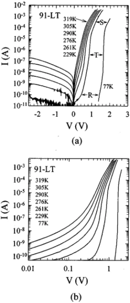
Figure 3共a兲 illustrates the temperature-dependent I – V characteristics of the 91-LT. Because the sample is a p – n junction, the forward current should arise from a double in-jection of carriers: Holes from p and electrons from n elec-trodes. We analyze this current conduction in a similar way
as reported in Ref. 9. Assuming that this injection process is governed by the deep levels which are acting as recombina-tion centers, the injected electron lifetime n is determined by the concentration pR of the empty centers: n
⫽1/pRthn and the injecting hole lifetime by the
concentra-tion nR of the occupied centers:p⫽1/nRthp according to
Lampert’s transport theory.15 Herein, assume the acceptors in the LT region have a high density, there are few free electrons in the conduction band, and most of the acceptors are in empty states, that is pRⰇnR. When the carriers are
FIG. 1. 共a兲 Structure of the 91-LT sample with In0.12Ga0.88As/GaAs MQW grown at a low temperature of 300 °C.共b兲 Structure of the 90-N sample with MQW close to the n-type region and was grown at 550 °C.共c兲 Structure of the 89-P sample with MQW close to the p-type region and was grown at 550 °C.
FIG. 2. The forward I – V characteristics at 77 K for 91-LT, 90-N, and 89-P samples. All three samples have 500m diameter in area.
FIG. 3. 共a兲 The I – V characteristics of the 91-LT sample as a function of temperature. 共b兲 The same I – V characteristics of the 91-LT sample but plotted on a linear scale.
8075
J. Appl. Phys., Vol. 87, No. 11, 1 June 2000 Chenet al.
when the acceptors are almost empty. The current will rise strongly with voltage关as illustrated ‘‘T’’ region in Fig. 3共a兲兴. This current will continue until it reaches the trap-free space-charge-limited point, beyond which the current increases as
j⫽98pVa
2
/d3. This is illustrated as the ‘‘S’’ region in Fig. 3共a兲, where⑀is the permeability andp is the hole mobility,
Va is the applied bias, and d is the thickness of the LT
region. However, it should be noted that the current conduc-tion in this ‘‘S’’ region could be caused by a series-resistance effect.
Due to thermal excitation, the density of the electrons in the LT region will rise at high temperature and the concen-trations of the occupied states will rise also. Therefore, the recombination process is no longer restricted to the n-LT edge but extends throughout the whole LT region. Under this condition, the current displays an exponential function in a way similar to the recombination current in a depletion re-gion with midgap defects. The observation of the ideality factor n being close to 2 for the I – V curves at high tempera-ture confirms that the current is dominated by this conduc-tion mechanism.
According to the Schockley–Read–Hall recombination theory, the recombination rate can be approximated by R ⫽n/20, where n⬇p⫽niexp(eVa/2kT) assuming a
recom-bination level near the midgap in the LT layer, ni is the
intrinsic carrier concentration, Vais the applied voltage, and 0⫽(n0⫹p0)/2 is the average recombination lifetime.
As-suming n⬇p and the recombination centers are all effective throughout the entire LT region, the recombination current under small bias can be approximated by
Jrec⬇edni
20
exp共eVa/kT兲,
where d⫽0.75m is the thickness of the LT region. By fitting the saturation current to the experimental data, an ac-tivation energy of about 0.7 eV was obtained. This indicates that the current is indeed attributed by the recombination current in the LT region since it is close to EG/2. By extrapo-lating the current to zero-voltage axis, we obtained 0 ⫽7.05⫻10⫺12s by using n
i⫽10
6cm⫺3at 300 K. It should
be noted that we might overestimate 0 here because the
effective recombination thickness must be smaller than the entire LT thickness. A comparison of this value with0⫽9
⫻10⫺10s from a p-i-n GaAs diode previously grown at a normal temperature of 600 °C,14 proves that this value is al-most two orders of magnitude smaller. This short lifetime is consistent with the existence of defect states in the LT re-gion.
Figure 4 illustrates that the reverse current at small volt-age under high temperatures is weakly voltvolt-age dependent and displays approximately ohmic behavior. This current conduction can be explained by the generation current via deep levels in the LT region. The slight rise in the current with voltage is attributed to an expansion in the effective width of the LT region. Figure 5 illustrates the Arrhenius plot for the reverse current at several different temperatures. An activation energy of 0.68 eV is obtained for V⫽⫺0.1 V from the slope of each curve and it decreases slightly to about 0.65 eV for V⫽⫺0.5 V, probably due to field-assisted emission. This activation energy is close to half of the band gap of this material, suggesting that the reverse current is dominated by the generation current from midgap levels.
B. Capacitance–frequency„C – F…measurement
Figure 6 illustrates C – F spectra at⫺1 V for the 91-LT sample. The high-frequency plateau of about 30 pF, from a parallel-plate model, corresponds to the LT thickness. The trap occupation probability is modulated when a small oscil-lation signal is applied to the diode. If the signal frequency exceeds the trap’s emission time, the trap failing to follow this frequency will not change its charge state. Therefore, only the free carriers on both edges of the n and p regions can be modulated and the measured capacitance corresponds to the width of the total LT region. However, the portion of the traps with energy close to the quasi-Fermi level will al-ternately capture and emit carriers when the signal frequency FIG. 4. The reverse I – V characteristics of the 91-LT sample as a function of temperature.
FIG. 5. Arrhenius plot for the reverse current of 91-LT sample at several different temperatures.
is sufficiently low. The effective depletion width is reduced, resulting in a rise in the measured capacitance. Figure 6 il-lustrates that the capacitance increases from a high-frequency 30 pF to a midhigh-frequency 130 pF and further to a low-frequency 350 pF. The rise from the high- to midfre-quency value共corresponding to a parallel-plate thickness of 0.17m兲 suggests that a fast trap 共labeled as 91H兲 occupies at least a region of 0.75– 0.17⫽0.58m. The rise from the mid- to low-frequency capacitance共0.06m兲 suggests that a slow trap 共labeled as 91E2兲 occupies at least a region of 0.17– 0.06⫽0.11m. The emission time of the trap was determined from the inflexion frequency at which the capaci-tance step occurs.
The activation energy Ea and capture cross section
were then achieved by the slope of T2 as a function of 1000/T, yielding the results of 0.71 eV and 1.7⫻10⫺11cm2 for the 91H. However, the parameters for the 91E2 cannot be accurately resolved from the C – F spectra because the low-frequency plateau is not clearly defined. Their parameters will be obtained from DLTS measurement.
C. DLTS measurement
Because of the ill-defined nature of defect states in the LT region, we postulate three kinds of charges that could be swept out as based on the three capacitance plateaus in the
C – F spectra of Fig. 6: The free carriers on the edges of
electrodes as indicated by the high-frequency plateau, carri-ers emitting from the fast traps 共91H兲 located at about 0.17
m from one of the LT-electrode interfaces as indicated by the midfrequency capacitance plateau, and the carriers emit-ting from the slow traps 共91E2兲 located at about 0.11 m from the LT-electrode interface as indicated by the
low-frequency capacitance. Although a high low-frequency共typically 1 MHz兲 is normally chosen for DLTS measurement, the ca-pacitance transient related to the latter two cases could be observed in the DLTS measurement with time constants be-ing equal to the reverse of the inflexion frequencies.
Figure 7 presents the DLTS data taken at 30 kHz for all three samples. The 91-LT sample displays very strong sig-nals in contrast to very weak sigsig-nals previously found in
p-LT-n GaAs bulk structures,8 suggesting an enhancement in the signal visibility by the quantum confinement of carri-ers. Figure 7 depicts that the 91-LT sample has one majority-carrier trap, 91H, and two minority-majority-carrier traps, 91E1 and 91E2. However, trap 91E1 is overlapped by 91H. The pa-rameters of 91H was resolved without considering any influ-ence by 91E1, but were later slightly modified to provide the best fit for the 91E1. The fitting results are Ea⫽0.73 eV,
⫽4.6⫻10⫺11cm2 for 91H and E
a⫽0.43 eV, ⫽3.4
⫻10⫺17cm2 for 91E1, respectively. An E
a⫽0.71 eV with ⫽1.5⫻10⫺15cm2was obtained for the minority 91E2 trap.
As for 550 °C-grown samples, Fig. 7 illustrates that one ma-jority trap 89H 共Ea⫽0.74 eV with⫽1.4⫻10⫺11cm2兲 was
detected in sample 89-P and two majority traps at Ea
⫽0.70 eV (⫽3.5⫻10⫺11cm2) and E
a⫽0.77 eV (⫽8.2
⫻10⫺15cm2) were detected in sample 90-N. Table I
summa-rizes their results.
It should be noted that the terms of majority and minor-ity traps do not have their conventional meaning because the structures are not conventional n⫹– p or p⫹– n junctions. We use the term of majority 共minority兲 simply because the transient capacitance increases共decreases兲 with time. Let us clarify their meanings by a simple model. Considering elec-FIG. 6. C – F spectra at a bias of⫺1 V for 91-LT sample. FIG. 7. DLTS data with rate windows 6.4, 6.4, and 5.1 s⫺1for 91-LT, 89-P, and 90-N samples, respectively. The capacitance transient was measured at ⫺2.5 V bias and the filling pulse was set at 0.1 V with filling pulse time of 3 s.
TABLE I. Summaries of traps measured by DLTS for In0.12Ga0.88As/GaAs superlattice samples. Traps Kind Tp共K兲 Ea共eV兲 Cross section共cm2兲
91-LT 91H Majority 250 0.73 4.6⫻10⫺11 91E1 Minority 260 0.43 3.4⫻10⫺17 91E2 Minority 370 0.71 1.5⫻10⫺15 90-N 90H Majority 250 0.70 3.5⫻10⫺11 90E Majority 370 0.77 8.2⫻10⫺15 89-P 89H Majority 250 0.74 1.4⫻10⫺11 8077
J. Appl. Phys., Vol. 87, No. 11, 1 June 2000 Chenet al.
where ⌬Q1⫽qp⌬L1 and ⌬Q2⫽qn⌬L2. Combining the above equations, we obtain
⌬L1⫽
冉
Qt q p冊
L2 L1⫹L2 and ⌬L2⫽⫺冉
Qt qn冊
L1 L1⫹L2 . The total variation of the depletion width is given by兺
⌬L⫽⌬L1⫹⌬L2⫽ Qt q共L1⫹L2兲冉
L2 p⫺ L1 n冊
.If⌺⌬L⬍0, the transient capacitance increases with time and the DLTS signal behaves as a majority trap. On the other hand, if ⌺⌬L⬎0, the DLTS signal behaves as a minority trap. Because in our case, the n and p concentrations are about the same order of magnitude, it is possible to observe both the minority and majority traps depending on the rela-tive values of L1, L2, which in turn depend on the
param-eters of the traps.
Detail examination revealed that the traps 91H and 91E2 observed by DLTS were the high- and low-frequency traps observed in C – F spectra, respectively. The trap 91E1 was not detected in the C – F spectra, probably because it is over-lapped by 91H and the C – F spectra do not have high reso-lution for individual traps. The consistency between the
C – F and DLTS results indicates that the traps do not result
from any capacitance dispersion due to dielectric relaxation16 or any resistance–capacitance time constant effects.8,17 Moreover, the parameters of the traps can be more accurately determined because both methods detect traps at very differ-ent temperature range.
IV. DISCUSSION
Figure 8 shows the Arrhenius plot for the traps observed by C – F and DLTS measurement. The 91H trap共0.73 eV兲 is believed to be the same as the 90H and 89H traps. The in-tensity of this trap is much higher for the 89-P than for the 90-N sample as shown in Fig. 7, suggesting that this trap is a hole trap because the 89-P sample has its MQW region near the p-region and has stronger hole confinement. Since samples 89-P and 90-N were grown at 550 °C, this hole trap is not created solely by the LT growth although its intensity is largest in the LT sample. Therefore, it must be a common defect in a relaxed InGaAs/GaAs MQW. A possible origin of this trap is the strain relaxation due to a lattice mismatch between GaAs and InGaAs. We speculate that our samples are relaxed because their reverse-bias leakage current are more than two orders of magnitude higher than that of the
p-i-n GaAs bulk samples. A hole trap with an activation
energy of 0.67–0.73 eV was reported in relaxed InGaAs/ GaAs and was attributed to misfit dislocations.18 Ashizawa
et al.19 observed a trap H2 in their InGaAs/GaAs p⫹– n di-odes, whose position in the Arrhenius plot共Fig. 8兲 is close to our 0.73 eV trap. They attributed the H2 to the lattice mis-match between InGaAs and GaAs. Noting that the well width in the sample 90-N is different from the other two samples, indicating that a small variation in the well width does not introduce any significant difference in the param-eters of this hole trap.
The two minority traps at 0.71 and 0.43 eV detected in the 91-LT sample must be related to the LT growth because they were not observed in the 550 °C-grown samples. It is reasonable to deduce that these two traps are electron traps. Adding the activation energies of the 0.71 eV trap and the hole trap at 0.73 eV together renders a value of 1.44 eV that is near the band gap of GaAs at room temperature. This leads us to suspect that they may belong to the same trap. How-ever, the fact that the hole trap but not the 0.71 eV minority trap is discovered in the 550 °C-grown samples excludes the possibility that they belong to the same trap.
The 0.71 eV minority trap is expected to be the impor-tant trap that governs the current transport discussed previ-ously. As mentioned before, the I – V characteristics for the 91-LT display a trap-filled-limit current at a low temperature and a generation-recombination current at high temperature. The activation energy of 0.68 eV obtained for the reverse-bias generation current is close to the 0.71 eV. In addition, this midgap trap is speculated to be an important compensa-tion center. We can only refer to those traps reported from LT GaAs because there are few reports on the traps of LT-grown InGaAs/GaAs. A dominating midgap trap was usually detected in LT-grown GaAs, such as those reported by Look
et al.,11 by Goo et al.12 from their LT-grown M-i-n struc-tures, and by Shiobara et al.13from their Schottky diodes of LT GaAs. Our previous studies also observed a dominant level at 0.65 eV in LT-GaAs structures.14There are two lev-els in Look’s model: the most important compensation center at 0.7 eV and the other at around 0.5 eV to make the an-nealed LT GaAs highly resistive. Although our observa-FIG. 8. Arrhenius plot for traps observed in 91-LT, 89-P, and 90-N samples. The hollow squares are 91E2, the solid squares are 91E1 and hollow circles are 91H traps observed in 300 °C-grown 91-LT sample. The solid circles are 89H and solid triangles are 90H traps observed in 550 °C-grown 89-P and 90-N samples, respectively.
tions of 0.71 and 0.43 eV traps support their model, we can-not conclude that our 0.43 eV level is their 0.5 eV level.
V. CONCLUSIONS
Three traps with significant intensity, one majority trap at 0.73 eV and two minority traps at 0.71 and 0.43 eV, have been observed in a LT-grown In0.12Ga0.88As/GaAs MQW
sample. The 0.73 eV trap, which is also detected in 550 °C-grown samples, is believed to be a common hole trap in relaxed In0.12Ga0.88As/GaAs MQWs. Among the two traps
only observed in LT-grown samples, the 0.71 eV trap is expected to be the most important compensation center and the dominant deep level that governs the current–voltage characteristics.
ACKNOWLEDGMENTS
The authors are grateful to Dr. N. C. Chen for many useful discussions and would like to thank the National Sci-ence Council of the Republic of China for financially sup-porting this research under Contract No. NSC-87-2112-M-009-022.
1
D. C. Look, D. C. Walters, M. O. Manasreh, J. R. Sizelove, and C. E. Stutz, Phys. Rev. B 42, 3578共1990兲.
2A. C. Warren, J. M. Woodall, J. L. Freeouf, D. Grischkowsky, and D. T.
Mclnturff, Appl. Phys. Lett. 57, 1331共1990兲.
3J. F. Whitaker, Mater. Sci. Eng., B 22, 61共1993兲.
4R. Takahashi, Y. Kawamura, T. Kagawa, and H. Iwamura, Appl. Phys.
Lett. 65, 1790共1994兲.
5P. W. Juodawlkis, D. T. McInturff, and S. E. Ralph, Appl. Phys. Lett. 69,
4062共1996兲.
6
J. S. Tsang, C. P. Lee, S. H. Lee, K. L. Tsai, and J. C. Fan, J. Appl. Phys. 79, 664共1996兲.
7P. K. Bhattacharya, S. Dhar, P. Berger, and F. Y. Juang, Appl. Phys. Lett.
49, 470共1986兲.
8J. F. Chen, P. Y. Wang, and N. C. Chen, Jpn. J. Appl. Phys., Part 2 37,
L1238共1998兲.
9
J. Cheng, S. R. Forrest, B. Tell, D. Wilt, B. Schwartz, and P. Wright, J. Appl. Phys. 58, 1787共1985兲.
10J. F. Chen, N. C. Chen, S. Y. Chiu, P. Y. Wang, W. I. Lee, and A. Chin,
J. Appl. Phys. 79, 8488共1996兲.
11D. C. Look, Z.-Q. Fang, H. Yamamto, J. R. Sizelove, M. G. Mier, and C.
E. Stutz, J. Appl. Phys. 76, 1029共1994兲.
12
C. H. Goo, W. S. Lau, T. C. Chong, and L. S. Tan, Appl. Phys. Lett. 69, 2543共1996兲.
13S. Shiobara, T. Hashizume, and Hasegawa, Jpn. J. Appl. Phys., Part 2 35,
L1159共1996兲.
14N. C. Chen, P. Y. Wang, and J. F. Chen, J. Appl. Phys. 83, 1403共1998兲. 15M. A. Lampert and P. Mark, Current Injection in Solids共Academic, New
York, 1970兲.
16
R. K. Ahrenkiel, P. Sheldon, D. Dunlavy, L. Roybal, and R. E. Hayes, Appl. Phys. Lett. 43, 675共1983兲.
17
D. V. Lang, M. B. Panish, F. Capasso, J. Allam, R. A. Hamm, A. M. Sergent, and W. T. Tsang, Appl. Phys. Lett. 50, 736共1987兲.
18
A. Y. Du, M. F. Li, T. C. Chong, K. L. Teo, W. S. Lau, and Z. Zhang, Appl. Phys. Lett. 69, 2849共1996兲.
19
Y. Ashizawa, S. Akbar, W. J. Schaff, and L. F. Eastman, J. Appl. Phys. 64, 4065共1988兲.
8079
J. Appl. Phys., Vol. 87, No. 11, 1 June 2000 Chenet al.