JOURNAL OF LIGHTWAVE TECHNOLOGY, VOL. 24, NO. 10, OCTOBER 2006 3835
The Effect of Signal-Feeder Characteristic
Impedance on the Signal Injection Efficiency of
Electroabsorption Modulator Integrated Lasers
Cheng Guan Lim, Member, IEEE
Abstract—The signal injection efficiency of electroabsorption
modulator integrated lasers (EMLs) is improved to suit 10-Gb/s applications. For a typical EML module design with a conven-tionally designed 50-Ω signal feeder to meet the input return loss requirement for 10-Gb/s applications, a reduction in device capacitance of the electroabsorption modulator (EAM) section by 65% from its typical value is necessary. By optimizing the characteristic impedance of the signal feeder, the required 65% reduction in device capacitance of the EAM section is reduced to 45%, which would naturally lead to enhanced extinction ratio and optical output power. With the addition of a series 5-Ω thin-film resistor along the signal feeder, the device capacitance reduction of the EAM section is further reduced to approximately 33% of the typical value.
Index Terms—Electroabsorption modulator integrated lasers
(EMLs), electroabsorption modulators (EAM), impedance match-ing, input return loss.
I. INTRODUCTION
I
N OPTICAL fiber communications, the optical signal dis-perses and becomes distorted as it travels along the optical fiber. This dispersion in the optical fiber limits the transmis-sion distance. Therefore, a compact and cost-effective light source with a low wavelength chirp characteristics is highly desirable in long-haul optical fiber communications systems. For these reasons, the electroabsorption modulator integrated lasers (EMLs) have attracted attentions [1]–[5]. This type of laser consists of a distributed-feedback (DFB) laser with an integrated electroabsorption modulator (EAM). The DFB laser operates in a continuous-wave (CW) mode emitting constant optical power into the EAM. The amount of light absorbed by the EAM depends on the applied modulation signal, hence modulating the optical signal at the output of the modulator. Compared to the conventional DFB lasers, the EMLs have a linewidth enhancement factor (α-parameter) of less than 1 [2], whereas the former has a value ranging from approximately 3 to 4 [6]. Therefore, the EMLs are capable of longer transmission distance due to their low wavelength chirp characteristics.Manuscript received February 13, 2006; revised June 16, 2006.
The author was with the Department of Photonics/Institute of Electro-Optical Engineering, National Chiao Tung University, Hsinchu 30010, Taiwan, R.O.C. He is now with the Ultra-fast Photonic Devices Laboratory, National Institute of Advanced Industrial Science and Technology, National Institute of Ad-vanced Industrial Science and Technology (AIST), Tsukuba 305-8568, Japan (e-mail: C.G.LIM@ieee.org).
Digital Object Identifier 10.1109/JLT.2006.881473
Besides, the EMLs have a higher extinction ratio and modu-lation capability compared to directly modulated lasers.
One common problem with laser diodes (LDs) is signal reflection between the LDs and microwave signal sources. Signal reflection is detrimental as it degrades signal injection efficiency and causes signal distortion. To quantify input signal reflection, an input signal reflection coefficient is used, and it has the following definition [7]:
Γ = (Z − Zo)/(Z + Zo)
whereZ is the impedance of the device or the input impedance of the electrical network connected to the microwave system, and Zo is the characteristic impedance of the microwave sys-tem. Typically, LDs have an impedance of a few ohms, whereas microwave systems have a characteristic impedance of 50Ω. Therefore, input signal reflection is obviously a severe problem in optical fiber communications due to this large impedance mismatch. The usual practice to overcome this problem is to add a resistor in series with the semiconductor laser in order to increase the input impedance to around 50 Ω. However, to use this conventional method to reduce the input return loss of EMLs does not solve the entire problem. Although the input return loss is reduced in this way, the modulation capability of the EMLs is greatly degraded due to the required large value of the series resistor in order to meet the acceptable input return loss. Also, the operating voltage required to achieve the same extinction ratio is much higher than in the case where the series resistor is not used.
At high frequencies, maximum power transfer cannot be achieved unless the impedance of the load is a complex conjugate of the source impedance. Hence, stubs—reactive impedance-matching networks—are widely used in microwave communications to reduce input return loss and maximize power transfer [7]. However, stubs may not be applicable to 10-Gb/s EML modules due to their narrowband nature. Even if the input return loss requirement for 10-Gb/s EML modules can be achieved using cascaded stubs, it would be too complicated to be feasible. To incorporate the reactive impedance-matching effect to reduce the input return loss of 10-Gb/s EML with no complications, a simple approach will be proposed and illustrated in this paper. It will be shown that the incorporation of resistive and reactive impedance matching greatly enhances the signal injection efficiency of a 10-Gb/s EML module to an acceptable level.
Fig. 1. (a) Typical device structure of the EML [3]. (b) Equivalent electri-cal circuit of the EML. (Color version available online at http://ieeexplore. ieee.org.)
II. RESULTS
The EML consists of a DFB LD section that operates in the CW mode and an EAM section that either operates under zero bias or reverse bias. As shown in Fig. 1(a), the structure of the EAM section is made up of a layer of metal, silicon nitride, p-type indium phosphide, multiple-quantum-well (MQW) active region, intrinsic indium phosphide, n-type indium phosphide, iron-doped indium phosphide, and n-type indium phosphide. The MQW active region is made of alternating layers of indium gallium aluminum arsenide phosphide having a different com-position for the wells and barriers. Based on this structure, the equivalent electrical circuit for the EAM is derived [Fig. 1(b)]. In Fig. 1(b), R1 and R2 represent the device resistance and differential resistance, whereas C1 represents the capacitance of the MQW active region, C2 and C4 represent the capaci-tance of the intrinsic indium phosphide layers, and C3 and C5 represent the iron-doped indium phosphide layers. As the DFB is operated in the CW mode, it can be represented by a p-i-n diode [NLPIN1 as in Fig. 1(b)] connected to the EAM section via a resistor to represent the resistance of the isolation trench [R3 as in Fig. 1(b)]. The equivalent electrical circuit of an EML module based on the standard GPO 7-pin butterfly package is shown in Fig. 2(a), where CPW1 and CPW2 represent the coplanar waveguide on the package, where the RF connector is
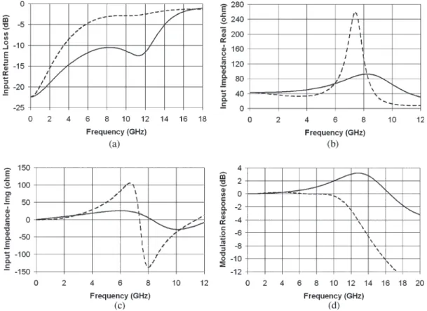
Fig. 2. (a) Equivalent electrical circuit of the EML module. (b) Input return loss response and (c) modulation response of a typical 10-Gb/s EML module. (Color version available online at http://ieeexplore.ieee.org.)
soldered and the signal feeder on the LD carrier/submount, re-spectively, L1 and L2 represent the inductance of the bonding-wire connecting the signal line and ground plane on CPW1 to the signal line and ground plane on CPW2, repectively, L3 represents the inductance of the bonding-wire connecting the signal line on CPW2 to the EAM, R4 is a thin-film resistor that regulates the input impedance close to the signal source impedance, and C7 is the equivalent capacitance of C1, C2, C3, C4, and C5.
For a typical 10-Gb/s EML module, the EAM has a de-vice resistance of 5Ω, a device capacitance of approximately 0.6 pF, a differential resistance of 300 to 500 Ω, a nominal value of 0.3 nH (± 0.1 nH) for L1 and L2, 0.4 nH (± 0.1 nH) for L3, and 50-Ω transmission lines (CPW1 and CPW2). As such, the 10-Gb/s EML module has the input return loss re-sponse and modulation rere-sponse shown in Fig. 2(b) and (c),
LIM: EFFECT OF SIGNAL-FEEDER CHARACTERISTIC IMPEDANCE ON SIGNAL INJECTION EFFICIENCY OF EMLs 3837
Fig. 3. (a) Real part and (b) imaginary part of the input impedance response of the typical 10-Gb/s EML module design shown in Fig. 2(a).
respectively. As can be observed, the input return loss is greater than−10 dB for frequencies above 3.4 GHz, and the modula-tion bandwidth is more than 12 GHz. Although the modulamodula-tion bandwidth requirement (i.e., more than 10 GHz) has been met, the input return loss is out of specification (i.e., the input return loss should be less than−10 dB for a frequency of up to more than 10 GHz). An inspection of the real part [Fig. 3(a)] and imaginary part [Fig. 3(b)] of the input impedance response reveals that the input impedance is inductive for frequencies below 7.4 GHz. The exponential increase in inductance with frequency causes a rapid and large increase to the real part of the input impedance that peaks at 7.4 GHz before decreasing rapidly when the imaginary part of the input impedance be-comes capacitive. To reduce the impedance mismatch to reduce input reflection, a natural and direct approach would be to reduce the device capacitance of the EAM section. Using this approach, it was found that the input return loss specification for 10-Gb/s applications can be met [Fig. 4(a)] comfortably by reducing the device capacitance of the EAM section to 0.21 pF (a reduction of 65% from the typical value). It can be noted from Fig. 4(b) and (c) that the impedance matching has been significantly improved as the real part and imaginary part of the input impedance have been controlled to within 40 to 93Ω and j26 to −j29 Ω, respectively, as opposed to 7.9 to 260 Ω and j106 to−j135 Ω for frequencies below 11.2 GHz, respectively. The modulation bandwidth was noted to widen significantly to 19.6 GHz [Fig. 4(d)]. However, the reduction in the device
capacitance of the EAM section requires the reduction in length and width as well as an increase in thickness of the MQW active region, and this requires compromises to be made on chirp, extinction ratio, and optical output power performance, hence, limiting the modulation speed and transmission distance. To lessen the impact of device capacitance reduction on the optical performance of the EAM, it is proposed here to optimize the design of the signal feeder on the LD carrier/submount to incorporate reactive impedance matching.
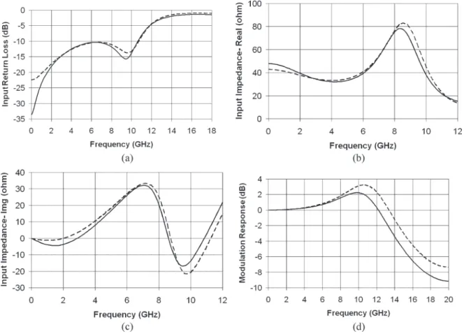
As observed in Fig. 3, the cause of input return loss rising above −10 dB at 3.5 GHz is due to excessive inductance of the input impedance. Hence, it is proposed here to de-sign the de-signal feeder on the LD carrier/submount to have a higher capacitive effect to counteract the excessive induc-tance of the input impedance over the appropriate frequency range. Following through rounds of optimization using the well-established commercial high-frequency computer-aided-design (CAD) package from Agilent Technologies—Advanced Design System, it was found that the highest possible device capacitance of the EAM section must not be more than 0.33 pF (a reduction of 45% from the typical value) and the optimum characteristic impedance of the signal feeder is 37Ω in order to meet the input return loss specification for 10-Gb/s applica-tions. As shown in Fig. 5(a), the input return loss would rise above −10 dB for frequencies above 5.3 GHz if the signal feeder has a characteristic impedance of 50Ω. However, with the signal feeder designed to have a characteristic impedance of 37 Ω, the input return loss stays below −10 dB for fre-quencies below 10.8 GHz. It was noted that the latter case has a signal injection efficiency ranging from approximately 68% to 79% compared to approximately 50% to 69%, as in the former case for a range of frequencies from 5.2 to 10.7 GHz. The minimum and maximum improvement in signal injection efficiency was noted to be approximately 3% at 5.2 GHz and 27% at 9.6 GHz, respectively. In comparison to the case where the device capacitance of the EAM section is reduced to 0.21 pF, this case has a narrower range of frequencies over which the input return loss is below −10 dB. In the former case, the range of frequencies over which the input return loss stays below −10 dB spans from dc up to 12.5 GHz. Also, due to the higher device capacitance of the EAM section compared to the former case, this case has a modulation band-width of 15 GHz [Fig. 5(b)] compared to nearly 20 GHz, as in the former case. Nevertheless, the latter case that uses the proposed approach allows the input return loss specification to be met by reducing the device capacitance of the EAM section by 45% of the typical value compared to 65% in the former case. This would lead to better optical performance (e.g., extinction ratio, optical output power, chirp, dispersion-limited modulation speed, and transmission distance) in the latter case.
By analyzing the input impedance responses [Fig. 5(c) and (d)], it can be noted that the input impedance has a smaller variation from the 50-Ω mark, a lower inductance for frequencies ranging from 2 to 7.5 GHz, a more gradual decrease in reactance from 7.5 to 9.7 GHz, and a lower capacitance. The above are the result of increased capacitive effect of the signal feeder [i.e., CPW2 as in Fig. 2(a)] that shifts the resonance
Fig. 4. (a) Input return loss response, (b) real part and (c) imaginary part of the input impedance response, and (d) modulation response of the 10-Gb/s EML module incorporating an EML with the device capacitance of the EAM section reduced to 0.21 pF. The responses shown as dashed lines are the responses prior to the device capacitance reduction of the EAM section.
Fig. 5. (a) Input return loss response, (b) modulation response, (c) real part and (d) imaginary part of the input impedance response of the 10-Gb/s EML module incorporating an EML with the device capacitance of the EAM section reduced to 0.33 pF, and a signal feeder with an optimized characteristic impedance of 37Ω. The responses shown as dotted lines are the responses for the case where the signal feeder has a characteristic impedance of 50 Ω.
LIM: EFFECT OF SIGNAL-FEEDER CHARACTERISTIC IMPEDANCE ON SIGNAL INJECTION EFFICIENCY OF EMLs 3839
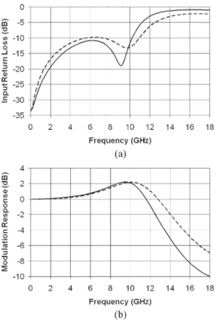
Fig. 6. (a) Input return loss response, (b) real part and (c) imaginary part of the input impedance response, and (d) modulation response of the 10-Gb/s EML module incorporating a signal feeder with an optimized characteristic impedance of 37Ω, a 5-Ω thin-film resistor along the signal feeder, and an EML with the device capacitance of the EAM section reduced to 0.4 pF. The responses shown as dashed lines are the responses for the case where the 5-Ω thin-film resistor along the signal feeder has not been added but with the signal-feeder characteristic impedance optimized to 37Ω and the device capacitance of the EAM section reduced to 0.33 pF.
of the capacitance of CPW2 and the parasitic inductance to a lower frequency (hence lower inductance for frequencies below 7.5 GHz) and away from that of C7 and the parasitic inductance (hence more gradual decrease in reactance and lower capacitance due to reduced combined effect of the capac-itance of CPW2 and C7). In the above illustration, the reactive impedance-matching technique was achieved by reducing the gap between the signal line and the coplanar ground planes to increase the capacitive effect of the signal feeder on the LD carrier/submount [i.e., CPW2 as in Fig. 2(a)]. For the microstrip transmission line, this can be achieved by reducing the thickness of the substrate.
Although the input return loss specification for 10-Gb/s ap-plication has been met in the above case (i.e., Fig. 5), the input return loss for frequencies below 3 GHz is still somehow high. To improve the input return loss for this range of frequencies, it is suggested to add a thin-film resistor with a resistance of 5 Ω along the signal line of CPW2 and in series with the EAM. By doing so, it was found that the device capacitance of the EAM section can be increased to 0.4 pF (a reduction of approximately 33% from the typical value) while meeting the input return loss specification and having better input return loss for frequencies below 3 GHz [Fig. 6(a)]. The optimum characteristic impedance of CPW2 in this case was found to be the same as in the previous case (i.e., 37Ω). In comparison to the previous case (i.e., Fig. 5), the real part of the input
im-pedance of this case is closer to the 50-Ω mark for frequencies below 2.9 GHz [Fig. 6(b)], which results in a lower input return loss for this range of frequencies. Due to the increased device capacitance of the EAM section that causes the resonance of C7 and the parasitic inductance to shift to a lower frequency, the input impedance is capacitive for the frequencies below 2.9 GHz [Fig. 6(c)]. Also, the modulation bandwidth was noted to decrease from 15 to 13.8 GHz [Fig. 6(d)].
To study the effects of the inductance of the bonding wires (i.e., L1, L2, and L3) on the input return loss, two different cases were investigated. The first case was to keep L1 and L2 at their nominal value (i.e., 0.3 nH) and vary the value of L3. The input return loss and modulation responses for the case where L3 has an inductance of 0.3 and 0.5 nH are shown in Fig. 7(a) and (b), respectively. It can be noted that the value of L3 has negligible effect on the hump of the input return loss response that peaks at slightly more than 6 GHz and that the frequency span of which the input return loss stays below −10 dB is reduced with increase in the value of L3 [Fig. 7(a)]. The modulation response was noted to have a higher resonant peak and a narrower modulation bandwidth when the value of L3 increases [Fig. 7(b)]. In the second case, the value of L1 and L2 was varied while keeping L3 at its nominal value (i.e., 0.4 nH). Consequently, the input return loss was found to be rather sensitive to the value of L1 and L2 throughout the spectrum [Fig. 8(a)]. As the value of L1 and L2 decreases below their
Fig. 7. (a) Input return loss response and (b) modulation response of the 10-Gb/s EML module incorporating a signal feeder with an optimized char-acteristic impedance of 37Ω, a 5-Ω thin-film resistor along the signal feeder, and an EML with the device capacitance of the EAM section reduced to 0.4 pF. The responses in solid line are the responses for the case where L3 has an inductance of 0.3 nH, whereas the responses shown as dashed lines are the responses for the case where L3 has an inductance of 0.5 nH.
nominal value, the input return loss for frequencies below 10 GHz increases, and the hump of the input return loss response eventually rises above−10 dB. When the value of L1 and L2 increases above their nominal value, the peak of the hump decreases, and the frequency span over which the input return loss is below−10 dB is reduced. The modulation response is, however, less sensitive to the value of L1 and L2 for frequencies below the resonant frequency [Fig. 8(b)]. For lower values of L1 and L2, the modulation bandwidth widens. Conversely, the modulation bandwidth is reduced when the value of L1 and L2 increases. Therefore, the capability of the automatic wire bonder must be evaluated, and the appropriate bond wire must be used to achieve the designed nominal value of L1, L2, and L3 in order to have high yield.
An implementation of the last case is shown in Fig. 9. As can be observed, there is no drastic change to the original design, except for the additional series thin-film resistor and a narrower gap between the signal line and the coplanar ground planes. Hence, this is indeed a straightforward and cost-effective ap-proach to improve the signal injection efficiency of EML by reducing signal loss due to input reflection.
III. CONCLUSION
For a typical EML module using a 50-Ω signal feeder, the device capacitance of the EAM section must not be greater than
Fig. 8. (a) Input return loss response and (b) modulation response of the 10-Gb/s EML module incorporating a signal feeder with an optimized char-acteristic impedance of 37Ω, a 5-Ω thin-film resistor along the signal feeder, and an EML with the device capacitance of the EAM section reduced to 0.4 pF. The responses shown as solid lines are the responses for the case where both L1 and L2 have an inductance of 0.4 nH, whereas the responses shown as dashed lines are the responses for the case where both L1 and L2 have an inductance of 0.2 nH.
Fig. 9. Schematic drawing of the proposed signal feeder on the LD car-rier/submount implemented using coplanar waveguide transmission line. The dc bias feeder for the DFB LD section has not been included.
0.21 pF (a 65% reduction from the typical optimum value) in order to meet the input return loss specification for 10-Gb/s applications. However, a reduction in device capacitance of the EAM section leads to degradation of optical performance (i.e., extinction ratio, optical output power, chirp, dispersion-limited modulation speed, and transmission distance). To lessen the compromises on optical performance, this paper has proposed a simple and easy-to-implement method to in-corporate reactive impedance matching on the LD carrier/ submount. The reactive impedance matching was achieved by optimizing the characteristic impedance of the signal feeder on the LD carrier/submount. Consequently, this approach yields an EML module design that meets the input return loss for
LIM: EFFECT OF SIGNAL-FEEDER CHARACTERISTIC IMPEDANCE ON SIGNAL INJECTION EFFICIENCY OF EMLs 3841
10-Gb/s applications with an EML of which the EAM section has a device capacitance of 0.33 pF (a 45% reduction from the typical optimum value). To improve the input return loss of the lower frequency regime, a series 5-Ω thin-film resis-tor was added along the signal line. As a result, the input return loss of the lower frequency regime was reduced substan-tially, and the device capacitance reduction of the EAM section was further reduced to approximately 33% of the typical opti-mum value. In comparison, the optimization of the signal feeder characteristic impedance leads to approximately 3%–27% improvement in signal injection efficiency of the EML module for a frequency range spanning from 5.2 to 10.7 GHz and helps to lessen the required device capacitance reduction for meeting the input return loss specification for 10-Gb/s applications. Improved high-frequency signal injection efficiency enables high-frequency components with lower power specifications to be used, hence reducing the capital and operation expendi-tures of the network provider. Also, improved high-frequency signal injection efficiency leads to better signal quality, hence lowering the bit-error rate and error vector magnitude, thereby improving transmission performance.
ACKNOWLEDGMENT
The author would like to thank the National Chip Imple-mentation Center, Taiwan, R.O.C., for the loan of the Agilent Technologies’ Advanced Design System—a well-established commercial high-frequency CAD package.
REFERENCES
[1] M. Aoki, M. Suzuki, H. Sano, T. Kawano, T. Ido, T. Taniwatari, K. Uomi, and A. Takai, “InGaAs/InGaAsP MQW electro-absorption modulator in-tegrated with a DFB laser fabricated by band-gap energy control selective area MOCVD,” IEEE J. Quantum Electron., vol. 29, no. 6, pp. 2088–2096, Jun. 1993.
[2] M. Aoki, N. Kikuchi, K. Sekine, S. Sasaki, M. Suzuki, T. Taniwatari, Y. Okuno, A. Takai, and T. Kawano, “Low drive voltage and ex-tremely low chirp integrated electroabsorption modulator/DFB laser for 2.5 Gb/s 200 km normal fibre transmission,” Electron. Lett., vol. 29, no. 22, pp. 1983–1984, Oct. 1993.
[3] E. Ishimura, Y. Miyazaki, K. Matsumoto, T. Takiguchi, T. Itagaki, D. Suzuki, K. Takagi, and H. Higuchi, “Small chirp and wide bandwidth integrated modulator-laser at zero offset-bias operation,” in Proc. 11th Eur.
Conf. Opt. Commun., Sep. 1997, vol. 2, pp. 171–174.
[4] Y. Miyazaki, H. Tada, T. Aoyagi, T. Nishimura, and Y. Mitsui, “Extremely small-chirp electroabsorption-modulator integrated distributed feedback laser diode with a shallow quantum-well absorption layer,” IEEE J.
Quantum Electron., vol. 38, no. 8, pp. 1075–1080, Aug. 2002.
[5] Y. D. Bae, B. K. Kang, B. Park, S. M. Lee, Y. H. Kim, H. K. Kim, M. K. Park, I. Kim, and D. H. Jang, “Operation of 1550-nm electroabsorption-Modulated laser at 40◦C for 10-Gb/s, 40-km transmis-sion,” IEEE J. Sel. Topics Quantum Electron., vol. 11, no. 1, pp. 135–140, Jan./Feb. 2005.
[6] K. Sato, S. Kuwahara, and Y. Miyamoto, “Chirp characteristics of 40-Gb/s directly modulated distributed-feedback laser diodes,” IEEE J. Lightw.
Technol., vol. 23, no. 11, pp. 3790–3797, Nov. 2005.
[7] D. M. Pozar, Microwave Engineering. Hoboken, NJ: Wiley, 2000.
Cheng Guan Lim (S’94–A’97–M’00) received the
B.Eng. (Honors) degree in electronic and electrical engineering and the Ph.D. degree from Institute of Microwave and Photonics, School of Electronic and Electrical Engineering, University of Leeds, Leeds, U.K., in 1997 and 2001, respectively.
From 2001 to 2003, he was a Research Engineer at the Yokohama Research and Development Labora-tories, The Furukawa Electric Company, Yokohama, Japan, working on the development of semiconduc-tor laser modules for digital and analog telecommu-nication applications. In 2003, he joined Agilent Technologies, Singapore, as a Senior Engineer, focusing on optoelectronic device manufacturing. From 2004 to 2005, he was a Senior Research Scientist at the Institute for Infocomm Research-Singapore (a member of the Agency for Science, Technology and Research-Singapore, and a National University of Singapore affiliated research institute) dealing with radio-over-fiber technologies. He was an Assistant Pro-fessor at the Department of Photonics/Institute of Electro-Optical Engineering, National Chiao Tung University, Hsinchu, Taiwan, R.O.C. Currently, he is a Re-searcher at the National Institute of Advanced Industrial Science and Technol-ogy, Tsukuba, Japan, where he conducts research on intersubband transitions in Sb-based quantum-wells for applications in ultrafast all-optical switching. His prime research interest is in theoretical and computational physics of advanced semiconductor nanodevices. His secondary research interests are photonic packaging, RF photonics, and photonic integrated circuits. He has one granted U.S. patent, one granted Japanese patent, written one invention disclosure, and he has published several international refereed journal and conference papers.
Dr. Lim has served as a Steering Committee Member for the Inaugural IEEE International Workshop on Antenna Technology 2005 in Singapore, and as a Technical Program Committee member for the 2005 Symposium on Technology Fusion of Optoelectronics and Communications-International Conference on Photonics in Taiwan. In 1995, he was awarded the Crab Tree Prize for outstanding academic achievement, the Hewlett–Packard Prize in 1997 for recognition as the best student in High-Frequency Engineering, and the F.W. Carter Prize in 2001 for presenting the best Ph.D. dissertation.