Solid-Stare Electronics Vol. 38. No. I. DD. 163-169. 1995 Pergamon 003&1101(94)EOO4tbJ Printed in Great Britain. All rights reserved Copyright 0’ I995 %&vier Science Ltd 0038-I 101195 $9.50 + 0.00
THE EFFECTS OF IMPURITY
BANDS ON THE
ELECTRICAL
CHARACTERISTICS
OF
METAL-SEMICONDUCTOR
OHMIC CONTACTS
YUNG-SONG Lou and CHING-YUAN WV
Advanced Semiconductor Device Research Laboratory and Institute of Electronics, National Chiao-Tung University, Hsin-Chu, Taiwan, Republic of China
(Received 1 I October 1993; in revised form 25 February 1994)
Abstract-The effects of semiconductor heavy doping on the I-V characteristics and the specific contact resistivity pc of semiconductor-metal ohmic contacts have been theoretically studied by incorporating the band-edge-tailing and impurity band effects. The Fermi level and the effective conduction band edge have been recalculated to determine the electron population and the bandgap narrowing. When the available electrons with higher transmission probability, which dominate the tunneling process, have been reduced by the presence of an impurity band, the tunneling current density becomes lower and hence the specific contact resistivity becomes higher for the case with the impurity band than that without the impurity band. Considering the physical properties inherent in a heavily-doped semiconductor, it is possible to explain the deviations of the experimental data from the theoretical results obtained from the conventionally used tunneling theory for the ohmic contacts. Furthermore, by comparing the simulated results and the measured pc data deduced from the Al and Ti contacts on both doping types of the Si-substrate, satisfactory agreements have been obtained.
1. INTRODUCTION
Rectifying and ohmic contacts have become increas- ingly important due to their wide applications in VLSI contacts and interconnections. As devices are scaled down to the submicrometer regime, parasitic series resistances, including the contact resistance and the diffusion sheet resistance, become serious[l,2]. Therefore, an understanding of the underlying physics of the ohmic contact is necessary in order to enhance the performance of scaled-down devices. As the doping concentration increases. the density of states in the conduction (or valence) band no longer obeys the conventional square-root law using the parabolic energy band and is dependent on the doping concentration. Due to the strong interactions either among the introduced impurities themselves or with the host lattice atoms, the discrete impurity levels broaden into a band, and the band tail gradu- ally moves into the energy gap, resulting in the well-known bandgap narrowing effects. The shape of the impurity band has been calculated by Morgan[3], and the band-edge-tailing has been calculated by Kane[4] and Bench-Bruyevich[S]. Although the ohmic contact is actually formed by depositing a metal layer on a heavily-doped semiconductor, the heavy doping effects have never been taken into consideration in the conduction mechanisms[6-81.
In this paper, the doping-dependent density of states is calculated by considering both the impurity band and band-edge-tailing effects. Then, the Fermi
level is obtained from the charge neutrality condition. The bandgap narrowing is determined by defining the effective band edge at an energy level above which 90% of the carrier population can be found, and such a definition is acceptable since good agreement be- tween the theoretical bandgap narrowing results and the experimental values obtained by Slotboom[9,10] is obtained. The electron population as a function of the electron energy considering the impurity band shows a serious departure from that with considering only the parabolic band, and different electrical prop- erties can be expected. In fact, by using the WKB approximation for the transmission probability of a quasi-free tunneling electron and the effective energy- momentum relation obtained from a known density- of-state function for the distorted band structure, the calculated tunneling current and specific contact res- istivity do show the predicted results. Based on our model, the detailed curves showing the specific con- tact resistivity vs the doping concentration are gener- ated for different Schottky-barrier heights on both types of the Si substrate. Besides, satisfactory agree- ments between the experimental results and the theor- etical calculations for pC have been obtained, which support the physical validity of our proposed model.
2. THEORETICAL BACKGROUND 2.1. High -doping effects
For a heavily-doped semiconductor, the discrete impurity levels in the energy gap may broaden into an
164 YUNG-SONG Lou and CHING-YUAN WV
impurity band. The splitting of the impurity energy level is due to the interactions between impurity atoms and valence electrons through the overlap of the wave function for the associated electrons. The density of states for the impurity band developed by Morgan[3] is:
Di(E) =
2N(2n6’)-‘lerp(
-(E
-&?j2),
(1)where N is the impurity concentration; E,, is the
donor energy level; 6 is the standard deviation of the impurity band given by:
6=q2
( >
$
3 II2.Jl s
in which t, is the semiconductor dielectric constant; 1 is the screening length of the Coulomb potential, which can be expressed as:
~=[$N)‘;“(~)‘:l]‘, (3)
where h is the reduced Planck constant; m,j‘ is the effective density-of-state mass. Note that the MKS- unit is used in this paper.
As the impurity concentration increases, the peri- odic potential of the host lattice is strongly disturbed through the interactions between host atoms and conduction electrons donated from impurity atoms. As a result, the conduction band is tailing gradually into the bandgap in a heavily-doped semiconductor, instead of a well-defined band edge for the density states in the lightly-doped semiconductor. The band- edge-tailing has been studied by Kane[4], and the modified density of states for the conduction band can be expressed as:
D (,)=m:(23’6)‘~’
c
n %’ y
(->
;6
’
(4) where 6 is shown in eqn (2) and u(x) can be expressed as: ’ y(_u)=&’ s (x -[)‘j2exp(-i1)dc. (5) %
In this paper, both the impurity band and band- edge-tailing effects are taken into considerations. The effective density-of-state function D(E) is given by the envelope of D,(E) and D,(E):
D(E) = max [Di(E),D,(E)]. (6)
Since the total number of states is assumed to be confined within a sphere in k space, the integration of
D (E) over the electron energy can yield the following
expression:
k(E)=[3n?j~zD(c)dtll;3. (7)
Equation (7) indicates that the effective energy- momentum relation for a heavily-doped semiconduc- tor can be obtained from the predetermined density-of-state function.
2.2. Electrical characteristics
For a heavily-doped metal/semiconductor (M/S) contact, the current density is dominated by the tunneling process, which can be expressed as[l 11:
s 4vb
J, = v.AF,(E) -
~m(~W,UGP (E) dE, (8)
0
in which v, is the carrier velocity in the direction of transport; F, and F,,, are the Fermi-Dirac distribution for semiconductor and metal, respectively. Appar- ently, due to the heavy doping effects, D(E) shows a serious departure from the conventionally used square-root law considering a parabolic band, and the electron population and hence the tunneling current due to the impurity band are quite different from those considering only the parabolic band. Moreover, the built-in potential Vb can be expressed as:
41/,=q~bn.o-qV+EFI-E’,, (9)
in which &n,O is the thermal-equilibrium barrier height; V is the applied bias; EFi and E i are the Fermi level and the effective conduction band edge consider- ing the heavy doping effects.
Since the density of states in an incremental energy range D (E )dE is equal to 2( 1/2n)‘dk, dk, dk: within an incremental volume in k space, eqn (8) can be rewritten as [ll]:
J, =
jjj q0.r IF, (E )
-F,ri(EWt(E,P
(
& 3dk& dk.
>
(10)
For a spherical energy surface with an isotropic density-of-state mass m z, eqn (10) can be further simplified as:J,=$ 4Yb a
jj [F,(E) -
Fm(EM’,(E.xW, dE.y, (11)
b0 0
in which A * is the effective Richardson constant; k, is the Boltzmann constant; E, = h 2k2,/2m $ and
El = h ‘k tj2m $ + ti2k 5 /2m $. Note that E1 is
measured from the potential minimum at the de- pletion edge. Under the conservation of total momen- tum, a relationship between E and E, + EL for a heavily-doped semiconductor can be obtained from eqn (7).
The transmission probability for a quasi-free elec- tron with an energy E, in the tunneling direction can be obtained by using the WKB approximation [6-81:
T,(E,)=exp
X (@b$ - (qvb -
&If
I>Effect of impurity bands on ohmic contacts 165 -f 0.6 > * ‘: 0.5 z z 0.4 0
n-Si m&r+, = I .06; Ed = -0.044eV - T=300K
10.5 -0.3 -0.1 0.1 0.3 0.5 E-EC, (eV)
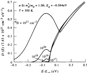
Fig. 1. The effective density of states for different doping concentrations.
where E,, can be expressed as:
The specific contact resistivity is defined as:
pc=
(
Z-F
yzo’
a,
-’I >
(13)
(14) which can be obtained by numerically differentiating eqn (8) with respect to the applied voltage V at zero bias and then taking its reciprocal value.
3. SIMULATION RESULTS AND DISCUSSIONS
Figure 1 shows the dependence of the effective density of states on the doping concentration. It is clearly shown that as the doping concentration in- creases above lOI cm-‘, the effective density of states deviates from the conventionally used square-root law and is dominated by the impurity band. When the impurity atoms are introduced, the Fermi level must adjust itself to preserve the charge neutrality. There- fore, the position of the Fermi level EF with respect to the conduction band edge of an intrinsic semicon- ductor EC, can be calculated from the charge neu- trality condition. Figure 2 shows the Fermi level as a function of the doping concentration. At higher doping concentrations. e.g. > 10” cmm3, the Fermi level considering the impurity band (EFi) moves toward the impurity energy level ED, due to the fact that Morgan’s result for a Gaussian-shaped impurity band contains 2N available states.
Due to the significant deformation of the conduc- tion band and the formation of the impurity band, the band edge is not exactly abrupt and the effective bandgap is reduced in a heavily-doped semiconduc- tor. The effective conduction band edge E: for high doping concentration is defined to be located at an energy level above which 90% of electron population can be obtained. The electron population is obtained by multiplying the effective density of states with the
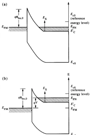
Fermi-Dirac distribution for the semiconductor at thermal equilibrium. Figure 2 also shows the effective conduction band edge with respect to E, as a function of the doping concentration. Clearly, our calculation results agree well with the experimental bandgap narrowing values obtained by Slot- boom[9,10]. Note that a discontinuity exists at a doping concentration of about 3 x 10” cm-‘, due to the transition of the effective band edge from the intrinsic band edge to the impurity band. Moreover, the physical properties of the Fermi level located within the allowed band, e.g. EFi > E 6, which is one of the major heavy doping effects for the parabolic band can be retained, as shown in Fig. 2 for the doping concentration higher than 4.5 x 10’8cm-3. Figure 3 shows the electron population as a func- tion of electron energy with respect of the Fermi level for different doping concentrations considering the impurity band and the parabolic band, respectively. As the doping concentration increases, the electron population will be controlled by the impurity band. Moreover, the electron population considering only the parabolic band accumulates in the energy regime higher than that considering the impurity band. The electrons located in the higher energy regime will exhibit higher transmission probability during the tunneling process, and hence a higher tunneling cur- rent and a lower specific contact resistivity can be expected. The energy band diagrams for a metal- n-type semiconductor contact considering the bandgap narrowing due to the heavy doping effects under thermal equilibrium and nonequilibrium are shown in Fig 4(a) and (b), respectively. Note that as the effective conduction band edge E i is deter- mined, the potential distribution within the depletion region can be obtained by using the depletion approximation.
Figure 5 shows the dependence of k on E for different doping concentrations, which may approach to the square-root law for doping concentration less
0.2 - n-Si m~lmo = I .06; Ed = -0.044eV T=300K
0.1 - . . experimental (Ref. [9. IO]) s‘ . -. . theoretical
-0.4 I I 1 I I 1
IO’5 IO’6 10” 10’8 IO’9 10ZO 102’ N, (cm-‘)
Fig. 2. The Fermi level EF, - E,, and the effective conduc- tion band edge El - EC, as a function of doping concen-
166 YUNGSONG Lou and CHING-YUAN WU
than 10”cm--‘. In view of eqn (11), the problem associated with the effects of impurity band on the tunneling current will concentrate on the calculation of a relationship between E and E, + EL. Note that only a low doping concentrations, E will be equal to
E, + EL as conventionally used for a parabolic band. The integration term in eqn (11) as a function of E,, i.e. (F, - F,)T,, still preserves the similar dependence on the doping concentration, as shown in Fig. 3. This fact indicates that the available electron population will determine the tunneling process and hence result in different electrical properties considering either the impurity band or the parabolic band. Therefore, the tunneling current considering the impurity band is smaller than that considering only the parabolic band, and hence the specific contact resistivity con- sidering the parabolic band is lower than that consid- ering the impurity band due to their difference in the available tunneling carriers. Note that except at very high doping level, e.g. N,, = 10” crnm3, the specific contact resistivity shows a bias-dependent property. This effect is further enhanced at lower doping con- centration and for higher Schottky-barrier height. In VLSI fabrication process, the Schottky-barrier height
(a) 0.025 F “E 2 0.020 ;; 0 a
,I
- n-Si m~/m, = 1.06; Ed = -0.044eV 7’ = 300 K ;’ *. : *. . . - impurity band I -0.10 -0.05 0 0.05 0.10 0.15 0.20 (b) E-E, (eV)0.6 - n-Si m~/mo = 1.06; Ed = -0.044eV T= 300 K 0.5 0.4 0.3 0.2 0. I 0 -0.4 -0.3 -0.2 -0. I 0 0.1 0.2 E-E, (eV)
Fig. 3. The electron population for different doping concen- tration. E FM E CO (reference energy level) E FN (b) E CO (reference energy level) EFN E’C EFM E VO
Fig. 4. The energy band diagram for the ohmic contact on a heavily-doped n-type Si substrate under (a) thermal
equilibrium and (b) nonequilibrium.
is dependent on the surface properties at the M/S interface which are strongly influenced by the process conditions, e.g. the ways of surface treatment, the methods of metal evaporation, and the damage due to either ion implantation or dry etching. Moreover, the surface doping concentration is generally altered by the improper thermal activation process, the dry etching, and the silicidation process. Therefore, the properties of the formed ohmic contact can be
1 .o - 0.8 -i g ei 0.6 0 -0.5 -0.3 -0.1 0. I 0.3 0.5 E$,(eV)
Fig. 5. The effective E-k relation for different doping concentrations.
n-Si m~/mo = 1.06; Ed = -0.044eV T=300K
_ - impurity band -. - -. parabolic band
highly deviated from those expected and are strongly dependent on the bias condition, especially when the impurity band effects are taken into account.
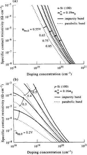
Considering the tunneling effective mass of elec- trons and holes for the (lOO)-oriented Si-sub- strate[ 121, the specific contact resistivity vs the doping concentration for different Schottky-barrier heights on both types of the Si-substrate are shown in Fig. 6. Clearly, the specific contact resistivity considering the impurity band is always higher than that considering only the parabolic band. Hence, a new method considering the physical properties inherent in a heavily-doped semiconductor is developed to explain the deviation of the experimental specific contact resistivity from the theoretical results obtained by using the conventional tunneling theory, which is quite different from those with tuning the tunneling effective mass and/or the Schottky-barrier height[7,8].
’
Qit(Vs) =
-4s
4 (E tit (4
Vs)dE
4. EXPERIMENTAL AND THEORETICAL COMPARISONS
where Vs is the potential drop across the semiconduc- tor surface depletion layer; Di,(E) = D f,(E) + D:‘,(E) is the sum of both types of the interface-state densities; and /I is used to quantitivatively specify the ratio of the density of the donor-like interface states to the total density of the interface states. For a metal/semiconductor Schottky-barrier contact with the interfacial layer, using the relationship among the potential drop across the interfacial layer, the metal work function &,, the electron affinity x, and &,,,O at thermal equilibrium, the fitted D,(E), 4b,o and Ci can be applied to solve the physical parameter /I. The thermal-equilibrium barrier height is assumed to be the same both on the lightly and heavily doped substrates if these M/S contacts are simultaneously processed, and the implantation damages can be fully eliminated after the thermal activation procedure. Thus, the physical parameters extracted from the (lOO)-oriented n -/n + and p -/p + Si epi-wafers
with the resistivity of 4-10Gcm for the epi-layer were used to fabricate the Schottky-barrier diodes. Other non-epi-wafers were also prepared to fabricate self-aligned Cross-Bridge Kelvin Resistor (CBKR) to minimize current crowding effects[l3]. Prior to loading into the vacuum system, the Schottky and the ohmic contacts received the same surface treat- ment in a diluted HF solution. Ti and Al were deposited by an E-gun evaporator. The I-V charac- teristics were measured by a HP4145B pA meter, and pc was deduced from a plot of the contact resistance vs the contact area. Moreover, the surface doping concentration was determined by SRP measurements.
The Z-V characteristics of a Schottky-barrier diode is analyzed by using the simple interfacial layer model developed by Tseng and Wu[14]. The thermal- equilibrium barrier height &,O (or +bp.O) and the interfacial-layer capacitance C, are first extracted from the measured reverse I-V characteristics since the net charge trapped in the interface states is kept unchanged under the reverse bias. Then, by substitut- ing the extracted &,,, and Ci into the theoretical majority carrier density based on the interfacial layer- thermionic emission-diffusion theory[ 151 and com- paring with the measured forward I-V characteristics, the Interface-State-Apparent-Spectra (ISAS) can be obtained. Moreover, the experimen- tally observed interface state density profile D,,(E) is fitted by a double-peaked density distribution function[ 161. (a) N^ 10-j - ‘z 6 10-4 - - impurity band x c -. - - parabolic band 4 1o-5 - 2 Qb”,O = E 3 10-6 - 6 8 2 10-7 - ._ k: 2 10-s I 10’8 10’9 1020 102’ Doping concentration (cmm3) (b) p-Si (100)
If the occupation function/;, for both the acceptor-
like and donor-like interface states are indistinguish- able, the net charge density trapped in the interface states can be expressed as:
I
10’8 10’9 1020 102’
Doping concentration (cme3)
Fig. 6. The specific contact resistivity vs the doping concen- tration for different Schottky-barrier heights on (a) n-type
and (b) o-tvoe S-substrates. ..*. <.
Effect of impurity bands on ohmic contacts 167
I
&+48
Dit(E)dE, (15) &- impurity band - -. - parabolic band
168 YUNG-SONG Lou and CHING-YUAN WV
(a)
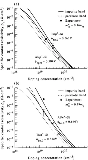
- impurity band . - -. parabolic band . Experiment I I I111111 I I Illllll IO'* 10'9 1020 Doping concentration (cmm3) (h) - impurity band -.-. parabolic band . Experiment I I I111111 I I I IllIll 10'8 10’9 1020 Doping concentration (cmw3)Fig. 7. The calculated and measured pC vs N, for AljSi and Ti/Si ohmic contacts on (a) p-type and (b) n-type substrates.
Schottky-barrier diodes can be directly applied to simulate the interface properties of the ohmic con- tacts. Details of the extraction and the computation procedures for these physical parameters can be seen in Ref. [16].
In general, the measured data of the contact resist- ance vs the contact area for the Al and Ti contacts on both types of the heavily-doped substrate are concen- trated around the line with a slope of - 1. This fact indicates that the parasitic current crowding effects have been minimized by using the self-aligned CBKR. The junction depth and the surface doping concen- tration are 0.2 pm and 4 x lOI cme3 for the p ‘/n junction and 0.3 pm and 1 x 10’9cmm3 for the n ‘/p
junction, respectively.
Using the extracted interface parameters, the sur- face doping concentration N,, and the tunneling effective mass m: for both types of (lOO)-oriented Si-substrates, the theoretical curves for pc vs Ns can be calculated, as shown in Fig. 7 for the Al and Ti contacts, respectively. For comparisons, the curves considering the effects of the impurity band and the parabolic band on pE are also plotted. Clearly, the measured pc vs N, data show more satisfactory
agreements with the theoretical results including the impurity band. This fact indicates that the high-dop- ing effects can not be neglected for a heavily-doped substrate. Although there still exist some uncertain- ties in accurately determining N, from the SRP measurement, it is shown that once the implantation damage can be fully eliminated by a thermal acti- vation process, the strongly process-dependent characterization parameter, e.g. &n.O (or &,O), should be carefully predetermined in order to clearly analyze the measured pc data. Moreover, only when +bn,O (or &,O) is first unambiguously determined, other effects which can result in the variations for pc, e.g. the modification of Ns due to the dry-etching process, the metal-silicon interaction, or the thermal silicidation[ 171, can be included and can be separately discussed without confusion.
5. CONCLUSIONS
The effective density of states for a heavily-doped semiconductor is calculated by considering the effects of both the impurity band and the band-edge-tailing. Using the developed model, the Fermi level is calcu- lated to determine the carrier population, and the effective band edge is redefined to obtain the bandgap narrowing and the potential distribution within the depletion region. Different electrical properties have been obtained for considering the parabolic band and the impurity band, which have been attributed to the difference in their distributions of electron popu- lation. Based on the WKB approximation for the transmission probability and the effective energy-mo- mentum relation obtained from a known density-of- state function, the tunneling current and the specific contact resistivity can be calculated. Moreover, the detailed curves showing the specific contact resistivity vs the doping concentration are generated for differ- ent Schottky-barrier heights on both types of the Si-substrate. Furthermore, based on the simple inter- facial-layer theory, the extraction methods for the interface parameters of the metal-semiconductor contact have been developed and applied to charac- terize both the Schottky-barrier diodes and the ohmic contacts in a self-consistent manner. Finally, by comparing the simulated results and the measured pC data deduced from the Al and Ti contacts on both doping types of the Si-substrate, satisfactory agreements have been obtained, which support the physical validity of our proposed model and characterization method.
Acknowledgements-The authors would like to express their sincere thanks to the National Science Council, Taiwan, Republic of China, for continuous grant support under the contract NSC-81-0404-E009-139.
REFERENCES
1. Y. EL-Mausy, IEEE Trans. Electron Devices ED-29,
Effect of impurity bands on ohmic contacts 169 2. K. K. Ng and W. T. Lynch, IEEE Trans. Electron
Devices ED-34, 503 (1987).
3. T. N. Morgan, Phys. Rev. 139, 343 (1965). 4. E. 0. Kane, Phys Rev. 131, 79 (1963).
5. V. Bench-Bruyevich, The Electronic Theory of Heavily Doped Semiconductors. Elsevier, New York (1965). 6. F. A. Padovani and R. Stratton, Solid-St. Electron. 9,
695 (1966).
7. A. Y. C. Yu, Solid-St. Electron. 13, 239 (1970). 8. C. Y. Chang, Y. K. Fang and S. M. Sze. Solid-St.
Elecrron. 14, 541 (1971).
9. J. W. Slotboom and H. C. De Graaff, Solid-St. Elec- tron. 19, 857 (1976).
0. J. W. Slotboom, Solid-St. Electron. 20, 279 (1977).
Il. J. W. Conley, C. B. Duke, G. D. Mahan and J. J. Tiemann, Phys. Rev. 150, 466 (1966).
12. K. K. Ng and R. Liu, IEEE Trans. Electron Devices
ED-37, 1535 (1990).
13. P. Cappelletti, M. Finetti, A. Scorzoni, I. Suni, N. Circelli and G. Dalla Libera. IEEE Trans. Electron Devices ED-34, 532 (1987).
14. H. H. Tseng and C. Y. Wu, J. uppl. Phys. 61, 299 (1987).
15. C. Y. Wu, J. appl. Phys. 53, 5947 (1982).
16. Y. S. Lou and C. Y. Wu, IEEE Trans. Electron Devices ED-41, 558 (1994).
17. Y. S. Lou and C. Y. Wu, Solid-St. Electron. 37, 353 (1994).