Formation of Branched ZnO Nanowires from Solvothermal Method and Dye-Sensitized
Solar Cells Applications
Hsin-Ming Cheng,†Wei-Hao Chiu,†Chia-Hua Lee,‡Song-Yeu Tsai,‡and Wen-Feng Hsieh*,† Department of Photonics and Institute of Electro-Optical Engineering, National Chiao Tung UniVersity, 1001 Tahsueh Road., Hsinchu 30050, Taiwan, Republic of China, and PhotoVoltaics Technology Center, Industrial Technology Research Institute, Hsinchu 310, Taiwan, Republic of China
ReceiVed: June 14, 2008; ReVised Manuscript ReceiVed: July 30, 2008
Branched ZnO nanowires have been fabricated on conductive glass substrates via a solvothermal method for dye-sensitized solar cells (DSCs). The 1D branched nanostructures can afford a direct conduction pathway instead of interparticle hops while using nanoparticles. Furthermore, the short-circuit current density and the energy conversion efficiency of the branched ZnO nanowire DSCs are 4.27 mA/cm2and 1.51%, which are twice as high as the bare ZnO nanowire ones. The improvement was a consequence of the enlargement of the internal surface area within the photoelectrode and allowed us to achieve higher dye adsorption to significantly enhance the performance of the DSCs.
I. Introduction
Dye-sensitized solar cells (DSCs) have exhibited solar energy-conversion efficiency of over 10% and remain one of the most promising candidates, as they possess advantages of being flexible, inexpensive, and easier to manufacture than brittle silicon solar cells.1,2 A very important feature of DSCs is the photoelectrode, which includes mesoporous wide-bandgap oxide semiconductor films with an enormous internal surface area, typically a thousand times larger than those of bulk films.3-5 To date, the highest solar-to-electric conversion efficiency has been achieved with films that consist of 20 nm TiO2 nanocrys-tallites sensitized by ruthenium-based dyes.1ZnO is a versatile, wide-bandgap semiconductor and has recently been reported as an alternative for DSCs because ZnO offers a large direct band gap of 3.37 eV, which is similar to TiO2and has very high electron mobility, which is about 155 cm2V-1s-1for high-quality thin film.6ZnO also can be tailored to various nano-structures as compared to TiO2, which provides a promising means for improving the performance of the photoelectrode in DSCs.7
Competition between the generation and recombination of photoexcited carriers in DSCs is a main bottleneck for developing higher conversion efficiency. 1D nanostructures, such as nano-wires8-10and nanotubes11-13have been extensively used, as the aim is expected to significantly improve the electron transport efficiency in the photoelectrode films by providing a direct conduction pathway for the rapid collection of photogenerated electrons and, therefore, reduce the number of interparticle hops. Furthermore, the immersion of a sensitizer into an array of nanowires with vertical pores should prove easier than the more tortuous pores of a nanoparticle film. However, insufficient internal surface area of those 1D nanostructures limits the energy conversion efficiency at a relatively low level, for example, 1.5% for ZnO nanowires8and 4.7% for TiO2nanotubes.12Another approach to overcome the problem was the incorporation of nanoparticles
with original 1D nanostructures.14,15 The nanowires/nanopar-ticles composite was mainly ascribed to enrich the light harvesting without sacrificing the electron-transport efficiency. Even so, the excess electron hoping through the interparticle barriers might still reveal the chance of charge recombination. In this regard, the nanostructures of tiny hierarchical nanobuild-ing units into larger organized conformations and geometrical architectures are intensely desirable from both the structural design and proposed application points of view. On the basis of the chemical vapor deposition (CVD), Suh et al.16and Baxter and Aydil17 have presented the dendritic ZnO nanowires and their efficiencies of about 0.5%. The relative low-energy conversion for the early reports was due to insufficient surface area of the branched ZnO nanowires. On the other hand, Kar and Santra18 recently fabricated the paint-brush-like ZnO nanostructures from the solvothermal approach and predicted the self-assembled hierarchical nanostructures could be ap-propriate not only in multiport contact probes but also are suitable for dye-sensitized solar cell applications because of their large surface areas. Moreover, Jiang et al.19reported the ZnO-nanoflower photoanode via a hydrothermal method and had the 1.9% efficiency in DSCs for which was the highest efficiency in ZnO nanowire-based DSCs to date. Accordingly, aqueous solution method is one of the remarkable approaches to fabricate functional and dense hierarchical ZnO nanostructures such as the photoelectrode in DSCs from the low cost and mass production requirements.
In the present work, we fabricated the treelike branched ZnO nanowire structures via a simple solvothermal method. The 1D secondary branches directly attached to the main ZnO nanowire backbone could simultaneously afford a direct conduction pathway and achieve the higher dye adsorption to significantly enhance the overall efficiency of the DSCs.
II. Experimental Section
Synthesis of Branched ZnO Nanowire Arrays. The branched ZnO nanowires were fabricated from a modified aqueous solution method similar to Law et al.8First, the arrays of ZnO nanowires were synthesized on seeded fluorine-doped tin oxide (FTO) substrates (10 Ω per square, Nippon Sheet Glass) by
* To whom the correspondence should be addressed: Tel: +886-3-5712121, ext. 56316. Fax: +886-3-5716631. E-mail: wfhsieh@ mail.nctu.edu.tw.
†National Chiao Tung University. ‡Industrial Technology Research Institute.
J. Phys. Chem. C 2008, 112, 16359–16364 16359
10.1021/jp805239k CCC: $40.75 2008 American Chemical Society Published on Web 09/25/2008
immersing the seeded substrates in aqueous solutions containing 0.08 M zinc nitrate hydrate (98%, Riedel-deHae¨n), 0.08 M hexamethylenetetramine (99%, Showa), and 12 mM polyeth-ylenimine (branched, low molecular weight, Aldrich) at 95°C for 10 h. Second, the ZnO nanowires substrate obtained from the first step were recoated with seed layers of ZnO nanoparticles by dip-coating in a 0.005 M zinc acetate dihydrate (Zn(OAc)2) (99%, Riedel-deHae¨n) in ethanol. Then the branched nanowires were grown by immersing the seeded ZnO nanowires in aqueous solutions containing 0.02 M zinc nitrate hydrate, 0.02 M hexamethylenetetramine, and 3 mM polyethylenimine at 95°C for 5 h. The branched ZnO nanowires were finally rinsed with deionized water and baked in air at 450°C for 30 min to remove any residual organics.
Cell Fabrication and Characterization. Solar cells were prepared by immersing the branched ZnO nanowires on conductive glass substrates into a solution of 0.5 mM cis-bis(isothiocyanato)bis(2,2′-bipyridyl-4,4′ -dicarboxylato)-ruthe-nium(II) bis-tetrabutylammonium (N719, Solaronix) in acetonitrile/
tert-butanol (1:1) for 20 min, and the films were then rinsed
with acetonitrile. The sensitized electrodes were sandwiched together with thermally platinized FTO counter electrodes separated by 25µm thick hot-melt spacers (Surlyn, Dupont).
The internal space of the cell was filled with an electrolyte solution (0.1 M LiI, 0.5 M 1,2-dimethyl-3-propylimidazolium iodide, 0.03 M I2, and 0.5 M tert-butylpyridine in acetonitrile). The area of active electrode was typically 0.28 cm2. Efficiencies for solar energy conversion and ac impedance spectroscopy were immediately evaluated under AM 1.5 simulated sunlight (Ya-mashita Denso, YSS-100A) with an electrochemical analyzer (Autolab, PGSTAT3). The light power was calibrated with a set of neutral density filters using a silicon photodiode (BS-520, Bunko Keiki).
Instrumentation. The morphologies and dimensions were characterized using a JEOL-6500 field emission scanning electron microscope (FESEM) operated at 5 KeV. The advanced microstructures of ZnO nanostructures were analyzed using JEOL JEM-2100F field emission transmission electron micro-scope (FETEM) operated at 200 KeV. The phases were characterized using a Bede D1 thin film X-ray diffractometer (TFXRD). Raman spectroscopy was carried out using a frequency-doubled Yb:YAG laser (λ) 515 nm) on a Jobin-Yvon
T64000 microspectrometer with a 1800 grooves/mm grating in a backscattering configuration. Dye loading was determined by detaching the dye from the ZnO photoelectrode surface with 0.1 M NaOH solution and measuring the optical absorbance with a Hitachi U-2800 UV-vis spectrophotometer.
III. Results and Discussion
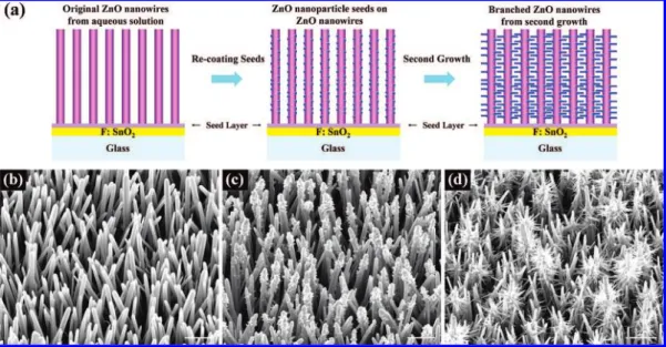
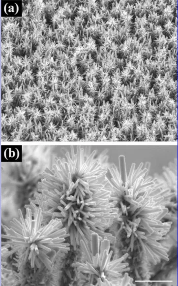
The formation mechanism of the branched ZnO nanowires is illustrated in part a of Figure 1 and its corresponding FESEM images in parts b-d of Figure 1. Part b of Figure 1 shows the bare ZnO nanowires with a slight vertical off-alignment were grown perpendicularly on the FTO substrate using a solvother-mal method. Through the precoating process on the ZnO nanowires, little crystalline nanopaticles with a diameter of 10-20 nm were formed on the backbone nanowires, as shown in part c of Figure 1. After the second growth step, radial secondary ZnO branches emanated from the seeds, as shown in part d of Figure 1. Figure 2 presents the large-scale and magnified FESEM micrographs of branched ZnO arrays. The branched ZnO nanostructures were fabricated over the entire substrate with a density of backbone nanowire about 7× 108 cm-2. The backbone nanowires have length and diameter in the range of 7-8µm and 150-250 nm, respectively, whereas
the secondary branches have length and diameter ranging from 100-300 nm and 20-50 nm, respectively. The branched ZnO nanowires can be fabricated by the infiltration of moderate concentrated Zn(OAc)2solution into interstitial voids between backbone ZnO nanowires. However, the secondary branches were not produced on the surface of each ZnO backbone. The lack of uniformity of secondary branches can be interpreted as the results of rough dip-coating processes that cause nonuniform infiltration and finally lead to randomly disturbed seed layers upon the backbone ZnO nanowires. Moreover, in some condi-tions, the seed layers hardly infiltrate into the deep side-wall of original ZnO nanowires during the immersion but left as coverage upon the ZnO nanowires (Supporting Information, Figure S1). Those failed conditions would mostly occur when using more concentrated Zn(OAc)2solution and also when the substrates were heated during dip-coating. The fast crystalliza-tion would lead the aggregacrystalliza-tion of ZnO seed layers and consequently blocked the infiltration of subsequent aqueous solutions.
Figure 1. (a) The schematic growth procedure from the original ZnO nanowires to the branched ZnO nanowires, (b) before and (c) after recoating a seed layer of the original ZnO nanowires obtained from a solvothermal method, and (d) the branched ZnO nanowires after second growth; scale bar, 1µm.
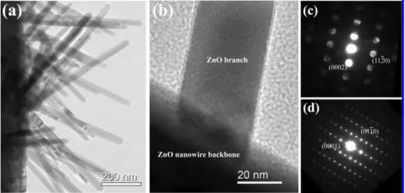
Further structural characterizations of the branched ZnO nanowires were performed with TEM. Unlike the other reports of comblike ZnO nanostructures, which demonstrated the monolithically single-crystalline relationship between the branches and backbone nanowires,20,21 in the present mechanism, the secondary ZnO branches were fabricated merely on the ZnO seeds regardless of the coordinate crystal relationship. Part a of Figure 3 displays the secondary ZnO branches, which were grown on the side walls of nanowire backbones with different radial angles. The evidence confirmed the secondary ZnO branches were not the derivatives of ZnO nanowires but definitely originated from the small crystallite ZnO seeds via our precoating process. The magnified intersection area of ZnO branch and nanowire was shown in part b of Figure 3. Parts c and d of Figure 3 show the corresponding nanobeam diffraction (NBD) of the secondary ZnO branch and select-area electron diffraction (SAED) of the ZnO nanowire backbone, respectively. The diffraction patterns confirmed the each ZnO nanostructure was preferentially oriented in the c axis direction with the single-crystal wurtzite structure even though the two components of ZnO nanostructures were not fabricated simultaneously.
Part a of Figure 4 shows theθ-2θ X-ray diffraction patterns
of ZnO nanostructures, which corresponds to the presence of hexagonal wurzite crystallites with cell constants of a ) 3.251 Å and c ) 5.208 Å. The strong {0001} diffraction family of ZnO indicates that the nanowires are moderately oriented in
the c axis direction. No excess peaks were detected, which indicates that all of the precursors have been completely decomposed. Because the wurtzite structure of ZnO belongs to the space group C64υ(P63mc), one primitive cell includes two formula units, with all of the atoms occupying 2b sites of symmetry C3ν. Group theory predicts the existence of the following optic modes: A1+ 2B1+ E1+ 2E2at theΓ point of the Brillouin zone; B1(low) and B1(high) modes are normally silent; A1, E1, and E2modes are Raman active; and A1and E1 also are infrared active. Thus, A1 and E1 are split into longitudinal (LO) and transverse (TO) optical components. Part b of Figure 4 shows a Raman spectrum of the branched ZnO nanowires, which was taken with an accumulation time of 120 s from a 5µm spot size excited by a frequency-doubled Yb:YAG
laser (λ ) 515 nm). As we can see, the remarkable E2(low) and E2(high) mode of ZnO are located at 98 and 438 cm-1, respectively. The peak at 332 cm-1 can be assigned to the second-order Raman scattering arising from zone-boundary phonons 2-E2(M) of ZnO. The weak and almost invisible signal around 581 cm-1is contributed to the superimposition of A1(LO) and E1(LO). No substrate signals appeared because of the penetration limitation of 515 nm laser light. The good crystalline quality of ZnO nanostructures confirmed above ensure that the photoelectrode can offer good electronic conductivity and avoid the electron trapping within the structural defects.
Part a of Figure 5 shows the compared photocurrent-voltage (J-V) characteristics for solar cells, constructed using the bare ZnO nanowires and the branched ZnO nanowires, with AM 1.5 illumination at 100 mW/cm2from a xenon lamp. The short-circuit current density (Jsc) and the overall light conversion efficiency of the branched ZnO nanowire DSCs were 4.27 mA/ cm2and 1.51%, respectively, which are almost twice higher than that of the bare ZnO nanowires. Table 1 summarizes the measured and calculated values obtained from each J-V curve. One factor for the increment in short-circuit current density would be the enhanced photon absorption associated with the presence of enlargement of internal surface area resulting in sufficient dye-loading. Although the length and density of ZnO structures exhibit the disadvantage compared with previous studies,8the overall efficiency can achieve almost the same value via utilizing the extra secondary nanobranches. The values of fill factor (FF) for ZnO DSCs are general lower than those using TiO2nanoparticles (0.6-0.7). This is attributed to recombination between photoexcited carriers in the photoanodes and tri-iodide ions in the electrolyte. A slightly different value in the bare ZnO nanowire and branched ZnO nanowire DSCs revealed almost the same interfacial recombination, which was evidenced by the equivalent value of the shunt resistance Rsh) (dV/dI)V)0 from the I-V curves under illumination. The series resistance
Rs)(dV/ dI)I)0for branched ZnO nanowire DSCs (25.64Ωcm2) was significantly lower than the bare ZnO nanowire ones (46.13 Ωcm2) and was previously explained association with the dye loading but not the nanowire length.10
Recently, electrochemical impedance spectroscopy (EIS) measurement has been widely performed to investigate elec-tronic and ionic processes in DSCs.22-28The Nyquist plots of the impedance data for bare and branched ZnO nanowire DSCs were performed by applying a 10 mV ac signal over the frequency range of 10-2 to 105Hz under illumination at the applied bias of Voc, as shown in part b of Figure 5. Some interior parameters of the devices with a thickness of LFcan be derived by well fitting the impedance data of the Nyquist plots to expressions based on the modified equivalent circuit of nanowire DSCs suggested by Wu et al.26,27In fact, the concrete equivalent
Figure 2. (a) Low- and (b) high-magnification FESEM images of the branched ZnO nanowires after second growth; scale bar, 1µm.
circuit might be more complex in the operation of the DSC devices. Mora-Sero´ et al. have recently reported a negative capacitance for different types of solar cells, that is, an inductive behavior that comes from the conductivity modulation of the electrolyte by injected electrons from the photoelectrode when providing high forward bias with low frequency.24Hence, the impedance data obtained at different applied potentials cannot be fitted with a single equivalent circuit. An essential component such as an inductive response was suggested to be considered
Figure 3. (a) TEM image of a single branched ZnO nanowire, (b) the magnified intersection area of ZnO branch and nanowire, and (c and d) the corresponding nanobeam diffraction (NBD) and select-area electron diffraction (SAED) for the secondary ZnO branch and the ZnO nanowire backbone, respectively.
Figure 4. (a)θ-2θ XRD profiles of A, the branched ZnO nanowires; B, the bare ZnO nanowires on the fluorine doped tin oxide substrate; and C, fluorine-doped tin oxide substrate only. (b) Raman spectra of the branched ZnO nanowires, using a frequency-doubled Yb:YAG laser (λ) 515 nm).
Figure 5. (a) Current density against voltage (J-V) characteristics and (b) Nyquist plots of the bare ZnO nanowires and the branched ZnO nanowire DSCs. The solid lines in (b) are the fitting results based on the equivalent circuit model (modified from ref 23) as shown in the inset. rwis the transport resistance of the electrons in the ZnO electrode;
rkis the charge-transfer resistance of the charge recombination between
electrons in the ZnO electrode and I3-in the electrolyte; The thickness
LFof all anodes are about 8µm; Cµ) (cµLF) is the chemical capacitance
of the ZnO electrode; Rsis a series resistance for the transport resistance
of FTO and all resistances out of the cell; ZN is the impedance of
diffusion of I3-in the electrolyte; RPtand CPtare the charge-transfer
resistance and the interfacial capacitance at the counter electrode (platinized FTO glass) /electrolyte interface, respectively; RFTOand CFTO
are the charge-transfer resistance and the interfacial capacitance at the exposed FTO/electrolyte interface, respectively; RFZand CFZare the
in series with a recombination resistance. To avoid the unneces-sary interference from the inductive behavior, we presently ignored the low-frequency part of impedance data. The fitted results were also listed in Table 1, which include the first-order reaction rate constant for the loss of electrons (keff), the electron lifetime (τ ) 1/keff), the electron transport resistance (Rw) rwLF) and the charge transfer resistance related to recombination of electron at the ZnO/electrolyte interface (Rk) rk/LF). We found
Rkand Rware quite similar for both DSCs in this present work, which indicated the same interfacial recombination and equal crystallinity for either bare ZnO nanowires or branched ZnO nanostructures. On the contrary, keff in the branched ZnO nanowire DSCs was smaller than the bare nanowire ones to cause the smaller effective diffusion length25 (Deff ) (Rk/
Rw)LF2keff) in branched ZnO nanowire DSCs. Because keff is related to reaction rate, the electron lifetime (τeff) 1/keff) could be prolonged by the additional transport distance between branches and conductive electrode.
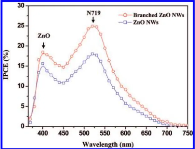
In general, the current density for DSCs is determined by the initial number of photogenerated carriers, the electron injection efficiency from dye molecules to semiconductor, and the recombination rate between the injected electrons and oxidized dye or redox species in the electrolyte. On the basis of the assumption of the same injection efficiency and recom-bination rate for the given ZnO DSCs systems, it is reasonable that the initial number of photogenerated carriers may be significantly affected by the variation in the light-harvesting capability of differently structured photoanodes. Figure 6 displays the wavelength distribution of incident monochromatic photon to current conversion efficiency (IPCE). The photocur-rent peaks occurring at approximately 400 nm were due to direct light harvesting by ZnO semiconductor, in which the photoge-nerated electrons diffused through ZnO and the holes in the valence band were replenished directly by charge transfer from the I3-/I-electrolyte.10The maxima of IPCE at approximately 525 nm are contributed by the dye absorption, corresponding to the visible t2fπ* metal-to-ligand charge transfer (MLCT). The IPCE obtained for the branched ZnO nanowire DSCs was
almost 1.5 times that of the bare ZnO nanowire. The improve-ment in the IPCE suggested that the high-energy conversion efficiency results predominantly from sufficient dye-loading by branched ZnO nanowires, which enlarged internal surface area within the photoelectrode. The dye loading of the photoelec-trodes was measured to determine the surface concentration of dye molecules adsorbed on different ZnO nanostructures (Sup-porting Information, Figure S2). The concentration of dye in the branched ZnO nanowire electrode was found to be 2.9× 10⁻⁹mol/cm-2as measured from dye-desorption experiments, which is almost 40% higher than the obtained value of 2.1× 10⁻⁹ mol/cm-2 for the bare ZnO nanowire electrode. It is important to note that the dye loading of the branched ZnO nanowires was not twice as high as the value of the bare ZnO nanowires, even though the current density and energy conver-sion efficiency of the branched ZnO nanowire DSCs are twice as high as the bare ZnO nanowire ones. The different could be ascribed to the insufficient internal surface of the bare ZnO nanowires and the excess dye, which resulted in the formation of Zn2+/dye complexes instead of the effective chemical bonding between ZnO and dye moleculars.29The shorter immersion time for deficient chemical-stability ZnO electrode as compared with TiO2electrode have recently been reported in detail by Chou et al.30Therefore, the excess immersion time for the insufficient internal surface of bare ZnO nanowires could not achieve more dye loading but seriously deteriorate the performance of DSCs. The concept of the branched nanostructures is anticipated to be applicable to other semiconductor photoelectrodes in organic-inorganic nanocomposite solar cells and branched heterojunction nanostructures for future applications. Although the secondary branches had nonuniform distribution, the branches emanated from partial ZnO nanowires because of the simple dip-coating process, and they still can offer greater effective surface area for dye adsorption than the bare nanowires. For optimization of the filling factor of the ZnO nanostructures, the dc or radio frequency magnetron sputtering and atomic layer deposition might be a great benefit to the precoating processes. Further improvement of energy conversion efficiency could be implemented through adjusting denser and longer branches to fill the interstitial voids between backbone nanowires, which will substantially improve light harvesting and the current density.
IV. Conclusion
In summary, branched ZnO nanowires have been fabricated on FTO substrates using a solvothermal method for DSCs. The short-circuit current density and the overall light-conversion efficiency of the branched ZnO nanowire DSCs were almost twice as high as the bare ZnO nanowire ones. The improvement can be explained in association with the enlargement of the internal surface area within the photoelectrode without increas-ing interparticle hops. In addition, the sufficient dye-loadincreas-ing in branched ZnO nanowire DSCs was further evidenced from the lower series resistance Rs ) (dV/dI)I)0 and dye-desorption measurement. The branched ZnO nanowires significantly en-hanced IPCE spectra as compared with the bare ZnO nanowires.
TABLE 1: Performances and Electron Transport Properties of the Bare ZnO Nanowire and the Branched ZnO Nanowire DSCs Determined by Photocurrent Density-Voltage (J-V) Characteristics and Electrochemical Impedance Spectroscopy (EIS) Analysis
ZnO DSCs Jsc(mA/cm2) Voc(V) FF η (%) keff(s-1) τeff(s) Rk(Ω) Rw(Ω) Deff(cm2/s)
bare nanowires 2.37 0.636 0.498 0.75 38.31 0.026 92.12 3.63 6.23× 10⁻⁴
branched nanowires 4.27 0.675 0.522 1.51 26.31 0.038 86.85 3.36 4.35× 10⁻⁴
Figure 6. Incident monochromatic photon to current conversion efficiency (IPCE) of the bare ZnO nanowire and the branched ZnO nanowire DSCs.
Therefore, the concept of these 1D branched nanostructures could simultaneously afford a direct conduction pathway and achieve higher dye adsorption to significantly enhance the overall energy conversion efficiency of the DSCs.
Acknowledgment. Authors acknowledge Dr. S. C. Lin (MCL/ITRI) for discussions and financial support from the National Science Council (NSC) of Taiwan (Project No. NSC-96-2628-M-009-001-MY3) and from PVTC/ITRI (Project No. 7301XS1K31).
Supporting Information Available: Cross section FESEM images of branched ZnO nanowires. Optical absorption of dye unloaded from the bare ZnO nanowire and the branched ZnO nanowire substrates. This material is available free of charge via the Internet at http://pubs.acs.org.
References and Notes
(1) Gra¨tzel, M. Inorg. Chem. 2005, 44, 6841.
(2) Nazeeruddin, M. K.; DeAngelis, F.; Fantacci, S.; Selloni, A.; Viscardi, G.; Liska, P.; Ito, S.; Takeru, B.; Gra¨tzel, M. J. Am. Chem. Soc. 2005, 127, 16835.
(3) Keis, K.; Magnusson, E.; Lindstrom, H.; Lindquist, S. E.; Hagfeldt, A. Sol. Energy Mater. Sol. Cells 2002, 73, 51.
(4) Stergiopoulos, T.; Arabatzis, I. M.; Cachet, H.; Falaras, P. J. Photochem. Photobiol. A 2003, 155, 163.
(5) Guo, P.; Aegerter, M. A. Thin Solid Films 1999, 351, 290. (6) Kaidashev, E. M.; Lorenz, M.; von Wenckstern, H.; Rahm, A.; Semmelhack, H. C.; Han, K. H.; Benndorf, G.; Bundesmann, C.; Hochmuth, H.; Grundmann, M. Appl. Phys. Lett. 2003, 82, 3901.
(7) Wang, Z. L. Materials Today 2004, 7, 26.
(8) Law, M.; Greene, L. E.; Johnson, J. C.; Saykally, R.; Yang, P. Nat. Mater. 2005, 4, 455.
(9) Baxter, J. B.; Aydil, E. S. Appl. Phys. Lett. 2005, 86, 053114.
(10) Pasquier, A. D.; Chen, H.; Lu, Y. Appl. Phys. Lett. 2006, 89, 253513.
(11) Wang, H.; Yip, C. T.; Cheung, K. Y.; Djurisˇic´, A. B.; Xie, M. H.; Leung, Y. H.; Chan, W. K. Appl. Phys. Lett. 2006, 89, 023508.
(12) Mor, G. K.; Varghese, O. K.; Paulose, M.; Shankar, K.; Grimes, C. A. Sol. Energy Mater. Sol. Cells 2006, 90, 2011.
(13) Zhu, K.; Neale, N. R.; Miedaner, A.; Frank, A. J. Nano Lett. 2007, 7, 69.
(14) Tan, B.; Wu, Y. J. Phys. Chem. B 2006, 110, 15932. (15) Ku, C. H.; Wu, J. J. Appl. Phys. Lett. 2007, 91, 093117. (16) Suh, D. I.; Lee, S. Y.; Kim, T. H.; Chun, J. M.; Suh, E. K.; Yang, O. B.; Lee, S. K. Chem. Phys. Lett. 2007, 442, 348.
(17) Baxter, J. B.; Aydil, E. S. Sol. Energy Mater. Sol. Cells 2006, 90, 607.
(18) Kar, S.; Santra, S. J. Phys. Chem. C 2008, 112, 8144.
(19) Jiang, C. Y.; Sun, X. W.; Lo, G. Q.; Kwong, D. L.; Wang, J. X. Appl. Phys. Lett. 2007, 90, 263501.
(20) Yan, H.; He, R.; Johnson, J.; Law, M.; Saykally, R.; Yang, P. J. Am. Chem. Soc. 2003, 125, 4728.
(21) Wang, Z. L.; Kong, X. Y.; Zuo, J. M. Phys. ReV. Lett. 2003, 91, 185502–1.
(22) Wang, Q.; Moser, J. E.; Gra¨tzel, M. J. Phys. Chem. B 2005, 109, 14945.
(23) Wang, Q.; Ito, S.; Gra¨tzel, M.; Fabregat-Santiago, F.; Mora-Sero´, I.; Bisquert, J.; Bessho, T.; Imai, H. J. Phys. Chem. B 2006, 110, 25210. (24) Mora-Sero´, I.; Bisquert, J.; Fabregat-Santiago, F.; Garcia-Belmonte, G.; Zoppi, G.; Durose, K.; Proskuryakov, Y.; Oja, I.; Belaidi, A.; Dittrich, T.; Tena-Zaera, R.; Katty, A.; Le´vy-Cle´ment, C.; Barrioz, V.; Irvine, S. J. C. Nano Lett. 2006, 6, 640.
(25) Adachi, M.; Sakamoto, M.; Jiu, J.; Ogata, Y.; Isoda, S. J. Phys. Chem. B 2006, 110, 13872.
(26) Wu, J. J.; Wang, D. K. P. AdV. Mater. 2007, 19, 2015. (27) Wu, J. J.; Chen, G. R.; Yang, H. H.; Ku, C. H.; Lai, J. Y. Appl. Phys. Lett. 2007, 90, 213109.
(28) Lin, C. J.; Yu, W. Y.; Chien, S. H. Appl. Phys. Lett. 2007, 91, 233120.
(29) Horiuchi, H.; Katoh, R.; Hara, K.; Yanagida, M.; Murata, S.; Arakawa, H.; Tachiya, M. J. Phys. Chem. B 2003, 107, 2570.
(30) Chou, T. P.; Zhang, Q.; Cao, G. J. Phys. Chem. C 2007, 111, 18804. JP805239K