透過光電化學蝕刻方式進行表面粗化以增加發光二極體之亮度
68
0
0
全文
(2) 透過光電化學蝕刻方式進行表面粗化以增加發光二極體之亮度 Enhanced Light Extraction of GaN-based Light-emitting Diodes with Selective Textured Regions by Photoelectrochemical Etching. 學生:傅健銘 指導教授:張國明 博士. Student:Jeng-Mign Fu Advisor:Dr. Kow-Ming Chang. 國 立 交 電子工程學系. 通 大 學 電子研究所碩士班. 碩 士 論. 文. A Thesis Submitted to Institute of Electronics College of Electrical Engineering and Computer Science National Chiao Tung University In Partial Fulfillment of the Requirements for the Degree of Master of Science In Electronics Engineering June 2005 Hsinchu, Taiwan, Republic of China 中華民國九十四年六月.
(3) 透過光電化學蝕刻方式進行表面粗化以增加發 光二極體之亮度. 研究生:傅健銘. 指導教授:張國明. 博士. 國立交通大學電子工程研究所. 摘要. 本論文將著重在光電化學蝕刻在氮化鎵上的特性探討和在發光二極體上的 應用,特性分析包括氫氧化鉀濃度, 過硫酸鉀濃度, 偏壓大小等變因對其之影 響。對於氫氧化鉀濃度而言,蝕刻速率主要受限在濃質擴散速率和水合反應所造 成峰值速率的影響,過硫酸鉀在鹼性溶液中所產生的激進分子將有利於蝕刻反應 中的氧化反應的進行,偏壓在此扮演的角色是改變氮化鎵其表面的能帶方向,且 其產生電洞井將有助於蝕刻速率的提升,氮化鎵上的金屬阻擋層能增進 UV 光所 產生的電子電洞對,但也會造成非均勻的蝕刻表面,可透過高偏壓方式來解決, 磷酸溶液的蝕刻機制一樣受限在濃質擴散速率和水合反應的影響,蝕刻後的表面 型態決定在光反應和電反應競爭後的結果。. 經過光電化學蝕刻處理過後的發光二極體,其漏電問題歸因於多層量子井旁 側壁遭蝕刻損傷所導致的漏電路徑。而粗化處理後所增加的亮度約為 1.1 至 1.3 倍,也約等於電力轉換光能所增加的值,光電化學蝕刻是個簡單且不需複雜的設 備的製程,蠻適合做氮化鎵為基礎的發光二極體表面粗化的製作。. I.
(4) Enhanced Light Extraction of GaN-based Light-emitting Diodes with Selective Textured Regions by Photoelectrochemical Etching. Student : Jeng-Ming Fu. Advisor : Dr. Kow-Ming Chang. Institute of electronics National Chiao Tung University. Abstract. In this thesis, a photoelectrochemical wet etching process has been discussed. The etching rate is mainly dominated by diffusion-limited and hydration effect about KOH concentration. The peaking effect in the PEC etch rate is analyzed by a hydration model. The chemical mechanism of the S2O82-/OH- etching of GaN as been found to involve either sulfate radical ions or hydroxyl radicals. Vary the direction of the band diagram by applying bias voltage can form a potential well for holes at surface and enhance the etching rate. The metal mask can enhance the etching activation but also cause non-uniform etching surface morphology. The non-uniform problems can be solved by applying higher bias voltage due to its high electric field. PEC etching in H3PO4. solution is also controlled by diffusion-limited and hydration effect. The. morphology after PEC etching is the result of competing between photo-assist and bias-assist etching. The leakage current of LEDs with PEC etching slightly increases owing to the damage of sidewall. The roughening treatment resulted in an increased of light output by a factor of 1.1~1.3 and the factor approximately equal the ratio of II.
(5) the luminance to electric power. The PEC etching technique is simple and does not require complicated process, implying that it will be suitable for manufacturing of GaN-based LEDs with surface roughening.. III.
(6) 誌. 謝. 首先,我要由衷的感謝張國明教授在這兩年來的關懷、指導和鼓勵,讓我在碩 士班的求學過程中不論是專業知識的涉獵或是在待人處事的道理等等諸多總 總,使我獲益匪淺,在此深表由衷感謝。同時感謝交大電子所博士班朱俊宜學長 與畢業學長鄭兆禎學長給予在實驗上或論文上的協助和指導,使得本論文能夠順 利完成。再來要感謝實驗室的學長和同學的幫助和砥礪,能進來張國明老師的實 驗室,才是這論文能夠完成的主要原因。. IV.
(7) Table of Contents Abstract (Chinese)……………………………………………………………………Ⅰ Abstract (English)……………………………………………………………………Ⅱ Acknowledgment (Chinese)………………………………………………………….IV Table of Contents…………………………………………………………………….V List of Figure…………………………………………………………………………Ⅵ. Chapter 1 Introduction………………………………………………………………1 Chapter 2 Experiment 2.1 Photoelectrochemical Etching Analysis of n-GaN…………………………..7 2.2 Applying PEC Etching on Selective Region of LEDs……………………….8 2.3 Scanning Electron Microscopy measurement……………………………....11 2.4 Atomic Force Microscopy measurement…………………………………...11. Chapter 3 Results and Discussion 3.1 The Analysis of Etch Depth………………………………………………...13 3.1.1 Effect of KOH………………………………………………………...13 3.1.2 Effect of Sulfate (K2S2O8)………………………………………….... 15 3.1.3 Effect of Bias Voltage………………………………………………...16 3.1.4 Effect of H3PO4 Etchant………………………………………………17 3.2 Mass Transport……………………………………………………………...18 3.3 Etching Surface Morphology…………………………………………….....20 3.4 Apply PEC Etching on Selective Region of LEDs…………………………21 3.4.1 Current – Voltage (I-V) Characteristics………………………………21 3.4.2 Current – Luminance (I - L) Characteristics……………………….....23. Chapter 4 Conclusion ………………………………………………………………………...24 Chapter 5 Future work………………………………………………………………………...25 V.
(8) List of Figures Fig. 1 Schematic diagram illustrate dislocation role in PEC etching of GaN……. Fig. 2 (a) Crystal structure and orientation of GaN. The inversion domain boundary (IDB) separating the two crystal domains laterally Fig. 2 (b) The polarization induced terminating fixed charges at the substrate interface Fig. 3 Schematic band diagram on surface band bending: (a)Ga-face and (b) N-face samples. Fig. 4 (a) The structure of GaAs-based LEDs with textured surface Fig. 4 (b) The structure of GaN-based LEDs with textured surface Fig. 5 The band diagram of n-type and p-type GaN in electrolyte Fig. 6 Structure of Samples Fig. 7 Plan-view of samples of experiment (a) I(b) II Fig. 8 Setup of PEC etching system Fig. 9 Spectrum of (a) Mercury-Xenon (Hg-Xe),and (b)Mercury (Hg) lamps Fig. 10 LEDs fabrication process Fig. 11 Photo-diode detector layout Fig. 12 Scanning electron microscopy instrument Fig. 13 Atomic force microscopy instrument Fig. 14 The etch depth of KOH concentration variation (a) 0V for 30 minutes (b) 1.5V for 10 minutes Fig. 15 The etch depth of K2S2O8 variation 0V for 30 minutes Fig. 16 The etch depth of bias voltage variation for 10 minutes. (a)0M (b) 0.01M K2S2O8 Fig. 17 Bend banding,(a)none (b) positive bias voltage. VI.
(9) Fig. 18 (a)The etch depth of PEC wet etching in H3PO4 etchant (0V for 30 minutes;1.5V, 3V for 10 minutes), (b)SEM image in H3PO4:H2O(1:15) etchant (0V) Fig. 19 KOH 0.01M, K2S2O8:0M,1.5V for 10mins (a) surface profile (b)(c)(d) SEM images Fig. 20 SEM images at KOH 0.1M and 0V bias voltage(a)0M (b) 0.01M (c) 0.05M K2S2O8 Fig. 21 SEM images at 2M KOH 0M K2S2O8(a)0V(b)1.5V(c)3V Fig. 22 Current-Voltage characteristic (a)log scale(b)forward I-V curve and dynamic resistance in KOH 2M etchant; (c)(d) in H3PO4:H2O=1:25 etchant Fig23. SEM images of the surface morphology, sample of experiment (a) I (b) II in KOH 2M and 3V bias; sample of experiment (c) I (d) II in H3PO4:H2O(1:5) and 3V bias Fig. 24 PEC etching in H3PO4 solution on samples ,(a)structure(b)plan-view,(c)(d) sidewall Fig. 25 (a) The luminance-current curve (b) the results after normalized Fig. 26 (Left: none PEC etching, Right: PEC etching),(a) cross-section structure (b) emission area, emission photography in (c) H3PO4 : water =1:5 (d) KOH 0.5M & K2S2O8 0M. VII.
(10) Chapter 1 Introduction. The development of device processing techniques in the III-nitride material system has been crucial to the subsequent rise of light-emitting diodes (LEDs), laser diodes, photodetectors, and transistors. Especially the study of GaN-based LEDs becomes be more interesting in blue, green, violet wavelength region of visible spectrum. As the result of the recent developments of GaN-based LEDs with increased brightness, applications including displays, traffic signals, exterior automotive lighting, and backlights for cell phones have become possible. In particular, an interest has developed concerning the use of white LEDs for general illumination using high-brightness. However, even though the brightness of visible/UV LEDs based on GaN-based materials continues to increase, the light output is still low compared to conventional light sources in high-flux lighting systems and it is necessary to further improve the light-output efficiency from LEDs [1]. Recently several methods of improving performance are investigated.. III-nitride semiconductors attract much attention for their wide application in electronic and optoelectronics devices. Due to the inert property of III-nitride semiconductors, it is not easy to etch the semiconductors by wet chemistry but by dry etching techniques. Dry etching techniques (such as reactive ion etching (RIE) [2], electron cyclotron resonance (ECR) RIE [3], inductively coupled plasma (ICP) RIE [4], low energy electron enhanced etching (LE4) [5], and chemically assisted ion beam etching (CAIBE) [6]) generally utilize a strong physical and a reactive chemical etch component, and the strong physical component would lead to ion-induced 1.
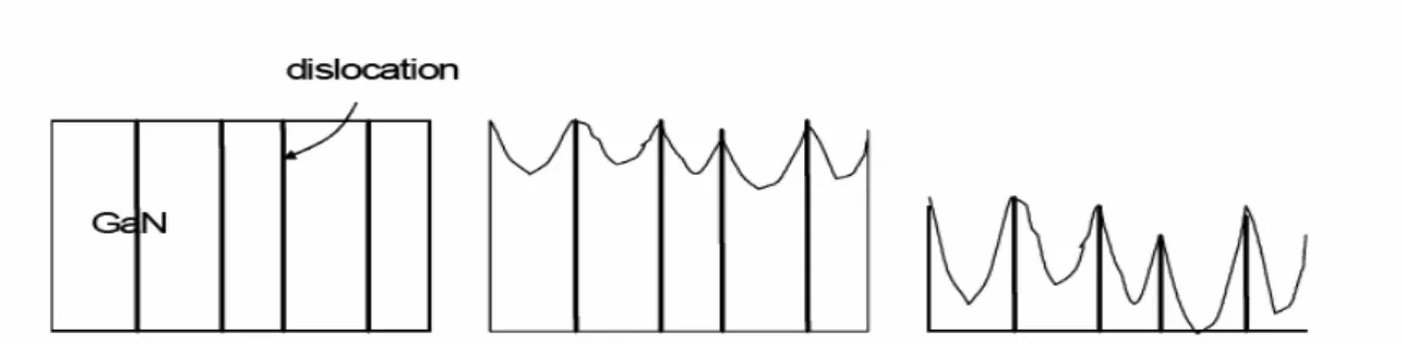
(11) damage of the semiconductor. Thus, it is necessary to develop low-damage etching techniques for III-nitride semiconductors. There are a lot of researches discussing the influence of methods, chemistry, and plasma composition on the etching rate and the morphology of etched surface.. It is important to explore wet etching techniques for the III-nitride materials since they can simplify processing and reduce damage to surface [7~9]. There are early reports of the wet etching of GaN in hot alkalis, in particular, NaOH, however only very low etch rates were achieved. In order to increase the etch rate, the technique of photoelectrochemical (PEC) etching is applied to III-nitride based materials . Several studies hypothesis that the photoelectrochemical (PEC) etching of GaN occurs through oxidative decomposion, in which photo-generated holes assist in the oxidation and subsequent dissolution of semiconductor into aqueous solution. The important reactions are [10]: 2GaN + 6h+ + 6OH- → Ga2O3(s) + 3H2O3 + H2O + N2↑ Ga2O3(s)+6OH-→2 GaO3-3(aq)+3H2O.. The extent to which dislocations are electrically active in GaN is currently an active research area [11~13]. Dislocations can serve as hole trap, and thus slow the etch rate of a PEC etching process. The morphology on etching surface suggest that the regions of high quality GaN are etched more rapidly, leaving the dislocations relatively unetched. The reduced etch rates at dislocations leading to whisker formation could arise through a number of different effects related to electrical activity at the dislocations. 2.
(12) Figure.1 illustrates the dislocation role in PEC etching of GaN. The formation of etching ridges and hillocks at crystal defects has previously been observed during the photo etching of other semiconductors such as GaAs, and has been attributed to the recombination of light-induced carriers at crystal defects. [14~16] The PEC etch process is highly sensitive to the spatial distribution of charges at the semiconductor surface, since anodic reactions require a concentration of holes at the semiconductor surface in order to convert surface atoms to higher oxidation states. The dislocations may introduce recombination centers, due to dangling bonds or impurities gotten from the bulk, which locally decrease the surface holes concentration. Hillocks or whiskers then result due to reduced etch rates at the crystal defects.. In the development of GaN wet etching, metal electrode is always severed as the catalytic in wet etching. The use of the Ti mask to enhance the photo-induced etching is based on earlier results from PEC etching of GaAs and InP. It has been previously determined that efficient extraction of photogenerated electron-hole pair can influence the etch rate for GaAs and InP [17]. The use of a metal mask that also serves as a contact to the material being etched, and that aids in the efficient extraction of electrons, can increase the etch rate substantially. As was the case for GaAs and InP, this also seems to be true for the GaN etched in these experiments. But it exists 2 disadvantages which are lateral potential gradient on the GaN film and a narrow region of operation for a smooth etched surface [18]. The lateral potential gradient was present along the distance from the conducting electrode to the GaN film; etching occurs to a non-uniform depth along the potential gradient. The oxidizing agent. 3.
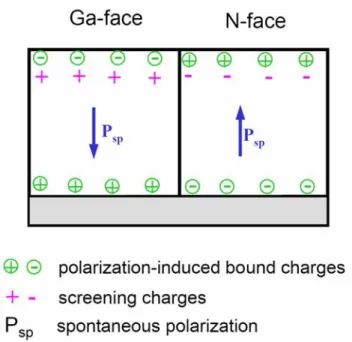
(13) peroxydisulfate (S2O82-) develops in electrodeless photo-assisted wet etching and replace the role of metal electrode [19]. Becasue the experiment has to measure the etching depth and apply the bias voltage, so the mask is needed.. Crystal polarity is one of the most important properties of wurtzite GaN because it significantly affects the electrical and optical properties of GaN films. The polarity of GaN also affects the wet etching rate [20~21]. The standard framework on the polarity of GaN was proposed that the Ga-face film is grown with [0001] orientation of the film, while the N-face film is grown with [0001] orientation. These two faces have different surface configuration, composition, and chemistry. For examples, a Ga face is typically smoother than a N face. Because of their polar axis, III-nitride crystals grown on a heterosubstrate can have two inequivalent orientations as shown in Fig. 2(a). In the case of GaN, these two orientations are refered to as Ga-face (N-face) polarity, depending on whether the Ga atoms (N atoms) of the Ga–N bilayers forming the crystal are facing towards the sample surface. In Ga-face samples, the crystallographic c-axis and the internal electric field point away from the substrate towards the surface, whereas the polarisation has the opposite direction. The polarisation-induced fixed lattice charges are negative at the surface and positive at the substrate interface as shown in Fig. 2(b). For N-face material, all charges and directions are inverted. The theoretical calculation [22] shows that the Ga-face film has larger surface band bending than the N-face film by about 3.5 eV due to the different spontaneous polarizations in both films, leading to the higher Schottky barrier height (SBH) of the Pt contact on Ga-face GaN than N-face GaN by 0.2 eV. The surface band bendings in the Ga- and N-face samples are as illustrated in Figs. (a) and (b)[23]. N-face GaN is essentially much chemically active than Ga-face GaN. Our. 4.
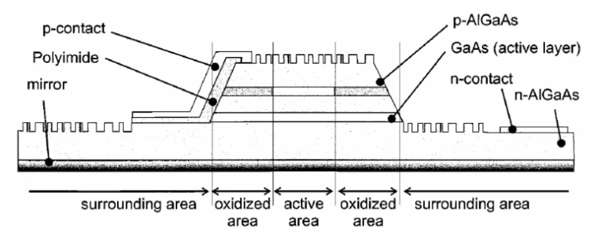
(14) etching process is carried out on conventional LEDs which is grown on Ga-face (Ga polarity). Therefore, the n-GaN sample of photoelectron chemical etching is also grown on Ga-face.. Fewer studies investigate the etching mechanism which is assisted with sulfate and applied bias, so the direction of experimental analysis emphasize on the relations of each others.. A special method of enhancing the light extraction is making the GaN film surface roughening [24~25]. According the refractive index of GaN (n=~2.5) and air (n=1) is different larger, the critical angle for the light escape cone is about 23 degree. Most light generated from MQW reflected by air above p-GaN and emit out from sidewall, backside finally. Total internal reflection at the semiconductor-air interface limits the light extraction per out-coupling surface to a few percent. Roughening the surface of LEDs is an alternative successful approach for improving the light extraction. The efficiency enhancement in surface-textured thin-film LEDs is generally [26] explained by scattering of the internally reflected light at the textured surface. Due to the resulting change in its propagation angle, the light gets multiple chances to escape from the semiconductor medium after reflections on the rear reflector of the LEDs structure. The method that produce roughened surface must give the appropriate surface morphology for efficient light extraction without damaging the electrical or optical properties. The textured surface has been achieved in GaAs-based LEDs by nature lithography, where a monolayer of randomly positioned polystyrene spheres acts as a mask for dry etching as shown in Fig. 4(a) [27].. 5.
(15) As mentioned previously about the dislocation discussion, the PEC etching ability to the dislocations and crystalline GaN has great difference in etching rate. By way of PEC etching, we can rougher the GaN surface. But the textured region of LEDs in the work is distinct from the GaAs-based LEDs. Figure. 4(b) shows roughening region in cross-section structure of LEDs. The PEC etching on p-type is not thinkable due to its thin thickness and the barrier to holes at GaN surface as shown in Fig. 5. So the area of etching surface in this work was Ga-face n-type GaN between adjacent conventional LEDs chips.. 6.
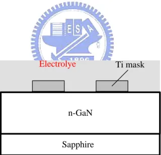
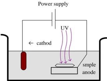
(16) Chapter 2 Experiment. 2.1 Photoelectrochemical Etching Analysis of n-GaN. The samples for this experiment were grown on Ga-face (0001) sapphire by metal organic chemical vapor deposit epitaxy (MOCVD). They consisted of 4 μm high quality n-GaN layer. Ti metal contacts were deposited by E-beam evaporator and patterned by standard lift-off techniques. The cross-section and plan-view of patterned samples are shown in Fig. 6 and Fig. 7(a). The Ti metal served to provide electrical contact to the samples as well as an etch mask. The Ti metal contacts were not annealed. The experimental apparatus of PEC etching is shown in Fig. 8. The PEC etching samples were clipped on the anode using a metal clip. A Pt wire was used as the system cathode. Several level of bias voltage is applied between the sample and the Pt cathode. The Mercury-Xenon (Hg-Xe) compact arc lamp provided constant UV light intensity about 25~35 mW/cm2. at 365 nm. The Hg-Xe lamp can involve better performance in PEC etching than Hg lamp according its peak illumination intensity at the wavelength that is smaller than 360 nm, the spectra of Hg-Xe and Hg lamp is exhibited in Fig. 9. Table. 1 shows the concentration of the alkaline (KOH), sulfate (K2S2O8), acid (H3PO4) electrolyte, and the conditions of applying bias voltage in this experiment. After a cycle of PEC etching process, the etch depth of samples were examined in a kosaka surface profiler measurement and taken the picture of the etching surface by optical microscope. The time length of a cycle is 200 seconds with 7.
(17) applying bias voltage or 600 seconds with no applying bias voltage .After 3 cycles process, the etching samples characterized using a Hitachi field emission scanning electron microscope (FE-SEM, s4000) and an atomic force microscope (AFM). The roughness data was measured by AFM over a 1 * 1 μm2 scan.. 2.2 Applying PEC Etching on Selective Region of LEDs. Samples in this work were grown by metal-organic-chemical vapor deposition. The epitaxial structure consisted of 4-μm-thick n-GaN 0.1-μm-thick InGaN–GaN (MQW) active layer, and 0.1-μm-thick p-GaN. Moreover, the carrier concentrations of the p-GaN and n-GaN were 5x10¹⁷ and 3x1018 cm, respectively. GaN-based LEDs with different conducting layers were fabricated. A wafer was cut into 2 parts, one part was the control group which followed the conventional LEDs process, and another part was the experimental group which carried out the PEC etching process. First, wafers were immersed in H2SO4:H2O2 solutions at 80℃ for 10 minutes in order to remove heavy metal ions and particles. Then a layer of Ni was deposited on the n-GaN surface by using E-beam evaporator and was patterned by standard lift-off techniques served to provide electrical contact to the samples as well as an etch mask. The Ni film (100nm) was not annealed. The plan-view of patterned appearance is displayed in Fig. 7(b). The patterned appearance in this part experiment is contrary to the first part. Next we used inductance-coupled plasma (ICP) to form the mesa structure due to both n- and p-type electrodes were formed on the same side of the epitaxial layer and the insulating properties of the sapphire substrates. The experimental group was carried out by PEC etching on uncoated Ni region and the control group did nothing. The etching time was controlled in 1~2 minutes, that 8.
(18) avoided the damage of the sidewall. The Ni film was removed by the HNO3 solutions. After PEC etching process, the wafers were cleaned in H2SO4:H2O2(3:1) solutions at 85℃ for 10 minutes in order to remove particles and photo-resister, and immersed in NH4OH:H2O(1:5) solutions at 75℃ for 10 minutes in order to remove chemical oxide. ITO (280 nm) was deposited on the p–In GaN/p–GaN samples by E-beam evaporator at 300℃ in oxygen ambience with a partial pressure of 5X10⁻⁴ torr. A step of photolithography was proceeded to define the current blocking layer (CBL). The purpose of CBL was due to some loss of light is inevitable as a result of photon absorption near the p-pad electrode. And another problem arising from the lateral structure of GaN-based LEDs involves current crowding around the p-pad electrode, depending on the electrical properties of the n-GaN layer and the light-transmitting layer [28].The higher contact resistance between Cr /p-GaN compared to the lower resistance between ITO/p-GaN is able to solve above problem. Remove the ITO of uncovered photo-resister area by HCL solutions. Next, to get better onmic contact in ITO and P-GaN, samples was alloyed at 440℃. The contacts were deposited by E-Beam evaporator (Cr/Au: 100nm/1400nm) and patterned by standard lift-off process. The chip size is 300*300μm2 and the distance of 2 adjacent chip is 50μm. The detailed fabrication process flow was listed as follows. 1. 2-inch p-i-n GaN wafers (MOCVD) were used in this experiment. Fig. 10(a) 2. Bare GaN wafers were performed by the standard RCA clean before barrier deposit or plasma activation in order to prevent particles staying on the wafers. 3. Photo-lithography: define the mesa region 4. Standard lift-off: deposite Ni by E-beam evaporator (100nm) and remove Photo-resister by ultrasonic shaker in NMP electrolyte. The Ni mask was formed. Fig. 10(b) 9.
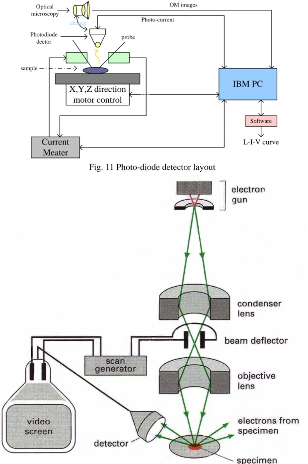
(19) 5. Form the mesa by using inductance-coupled plasma (ICP) and etch until n-GaN exposed. Fig. 10(c) 6. Perform the PEC wet etching for 1~2 minutes in experiment group. Fig. 10(d) 7. Remove Ni film: immersed in HNO3 solution.Fig. 10(e) 8. Wafer clean in H2SO4:H2O2(3:1)/85℃/10 minutes NH4OH:H2O(1:5)/75℃/10 minutes 9. Transparent Conducting layer(TCL): ITO(280nm) was deposited by E-beam evaporator 10. Photo-lithography : Define current blocking layer region 11. Remove ITO of uncovered PR region in ITO etchant for 2~3 minutes. Fig. 10(f) 12. Remove PR 13. TCL alloy at 440℃ 14. Clean. H2SO4:H2O2/80℃/10 minutes. 15. Photo-lithography : Define electrode area 16. Standard lift-off: deposit Cr/Au (100nm/1400nm) by E-beam evaporator and remove Photo-resister by ultrasonic shaker in NMP (75℃) electrolyte. The contact was formed. Fig. 10(g) 17. Clean. H2SO4:H2O2/80℃/10 minutes. 18. Measurements All electrical and optical properties of the LED performance were evaluated via on-wafer probing of the devices. The current-voltage (I - V) characteristics were measured using a parameter analyzer (HP 4156A) at room temperature. The sweep voltage was 0V to 5V at forward condition and 0V to -10 V at reverse condition. The light output power of the LEDs was measured using a photodiode detector as 10.
(20) shown in Fig. 11. The etching samples characterized using a Hitachi field emission scanning electron microscope (FE-SEM, s4000) and an atomic force microscope (AFM). The roughness data was measured by AFM over a 1* 1μm2 scan.. 2.3 Scanning Electron Microscopy measurement A scanning electron microscope (SEM) creates high resolution, three dimensional images of a sample’s surface. The sample, often gold-coated for electroconductivity, is bombarded with a focused beam of electrons which liberates secondary electrons from the sample’s surface. A detector in the microscope systematically “counts” these electrons, recording data on their origin and emission intensity which can then be assembled into a high contrast, high resolution image. The microscope also features a Kevex electron dispersive x-ray spectrometer (EDX) which can be used to ascertain the elemental composition of the portion of a sample being visualized. When a sample is struck by the SEM’s electron beam it emits x-rays which are picked up by the EDX. Because each element emits x-rays of characteristic energies and wavelengths, the EDX unit is able to determine which element is responsible for the emission. These data can be overlaid onto an SEM image to produce a virtual elemental map of a sample’s surface The diagram of SEM instrument is show in Fig. 12.. 2.4 Atomic Force Microscopy measurement. The atomic force microscope (AFM) is an essential tool for imaging surfaces in 11.
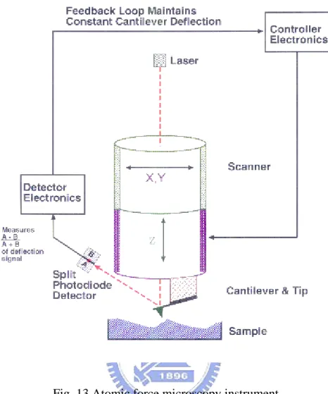
(21) applications in cell biology and biomaterials science, measuring surface topography on a scale from angstroms to 100 microns. The key component of the AFM is its cantilever. At the end of the cantilever is a tip that is used to sense a force between the sample and tip. The tip is held several nanometers above the surface using a feedback mechanism that measures surface-top interactions on the scale of nano-Newtons. The tip is brought into continuous or intermittent contact with the sample and raster-scanned over the surface. Continuous contact is referred to as Contact Mode, while intermittent contact is referred to as Tapping Mode. The height of the sample is measured by continuously scanning the sample and recording the deflection of the cantilever. Three-dimensional topographical maps are constructed by plotting the local height against the horizontal probe tip position. Nano-scale force interactions represent a developing area of study within the life sciences. The AFM can record the amount of force felt by the tip when brought close to and/or indented into the sample surface and then pulled away. The force is measured as a function of the deflection of the tip on the cantilever. This technique can be used to measure the attractive or repulsive forces between the tip and the sample surface, revealing chemical and mechanical properties like adhesion and elasticity. The diagram of AFM instrument is shown in Fig. 13.. 12.
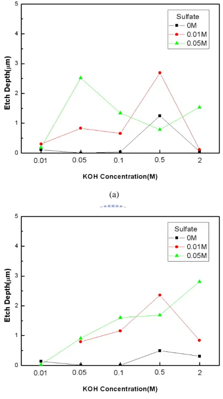
(22) Chapter 3 Results and Discussion. 3.1 The Analysis of Etch Depth 3.1.1 Effect of KOH. As the Fig. 14(a) shown, the etch depth has a peak appearance versus the KOH concentration (Bias: 0V, K2S2O8: 0M). We observed a peak etch depth of 1.25μm in the KOH 0.5M solutions. The OH- in both PEC oxidation and oxide dissolution reaction plays a reactant role, and the 1st reaction product (Ga2O3(s)) is just the 2nd reaction reactant. Generally speaking, if the amount of chemistry reactant is greater than the amount of product, it is tend to the positive reaction. And according the mass transport rule, the diffusion rate changes into fast in higher concentration and can accelerate the 1st reaction. But experimental results seem be not as we expect. However, the observation of a peak etch depth indicates that both of the solute (KOH, K2S2O8) and the solvent (H2O) play an important role in the PEC etching of GaN. In the 0.01M and 0.05M K2S2O8 conditions(0V bias) also shows the same results, but the KOH concentration of maximum etching depth in 0.05M K2S2O8 condition reduced to 0.05M. So we suppose that it may be related to H2O molecular about the result. Indeed, peaking in the wet chemical etching is a well-known phenomenon [29]. It has been reported in an electrochemical etching [30] or a thermal etching process [31]. Before a recent report by Quinlan which indicates a competing effect due to the 13.
(23) photo-reduction of hydrogen ions could result in similar effects [32], it is less noticed in the PEC etching process. Such an effect is attributed to a hydration effect in which competing effects from free water molecules (H2O)f and hydroxyl ions(OH-) produce a peak in the etch depth. The hydration effect model for analyzing PEC etching of GaN has been reported. In this model, both the free water molecules (H2O)f and hydroxyl ions(OH-) is needed to accomplish the etching[33]. The hydration effect means that if the more OHconcentration, the less (H2O)f concentration. And so does sulfate (K2S2O8). The two competing effects therefore produce a peak in etch depth whose location is very sensitive to the mean hydration number of solute. A general reaction rate equation is proposed by PENG et al. [34] to account for the GaN PEC etch rate ie., R=C。[H2O]rf[OH-]s In the equation, the factor C(λ, I, Ea, T) is a function of the incident photon wavelength, illumination intensity, activation energy of the reaction, and temperature, respectively. Hence we can infer the shift of peak location at 0.05M K2S2O8 that is due to water hydrate the sulfate and reduce amount of free water molecular. Due to oxidation and oxide dissolution reaction in PEC wet etching, the slow etch rate at low KOH concentration is caused by [OH-] that not enough to dissolve the oxide. On the contrary, the high KOH concentration makes a few [H2O]f and holes which is generated from UV light also become insufficient. The first oxidation reaction can not drive the second oxide dissolution reaction. The factor brings about the less etch rate at high KOH concentration. Fig. 14(b) shows etch depth of applied bias voltage. It is clearly detected that the maximum etch depth at 0.05M K2S2O8 is 3.02μm, but it is not located at 0.5M 14.
(24) KOH. It means that the dominated mechanism changes from photo-assist into bias-assist etching (holes injection). And the photo-generated holes will not govern etching actions in the conditions. Owing to the reactant (holes) is sufficient, the etch rate becomes proportional to the KOH concentration.. 3.1.2 Effect of Sulfate (K2S2O8). The photochemistry of peroxydisulfide has been extensively studied [35~37], and the relevant reactions for UV photoenhanced etching are summarized in Table. 2[38~39]. As Table. 2 shown, as time goes on, the K2S2O8 will be consumed as well as KOH .In order to consider the influence of K2S2O8 in etching reaction, the dose of K2S2O8 in the experiment were set in none, not saturation, over-saturation. At wavelengths shorter than ~310 nm, peroxydisulfate absorbs photons, resulting in the initial production of the sulfate radical (SO4-*), reaction (4), Table. 2. Depending on the pH of the solution, this radical either recombines, or results in production of the hydroxide radical (OH*) [in alkaline deaerated solutions, reaction (5)], or production of theoz onide (O3-) [ inalkalineaerated solutions, reaction (8)]. Both the sulfate radical ion and the hydroxide radical are very strong oxidizing agents, and thus could be involved in the photoenhaced wet etching of GaN, through reactions(6) and (7), Table. 2. The presence of peroxomonosulfate or of any other strong oxidizing product was checked with a test of iodide oxidation rate [40]. It should be noted that S2O82does not absorb at 365 nm. Figure. 15 shows results of the etch rate versus K2S2O8 concentrations. The low etch rate at low KOH concentration which is caused by 15.
(25) diffusion-limited can be enhanced with K2S2O8. The generated hydroxyl radical and sulfate ion radical assist the first oxidation reaction and then promote overall etch rate. The etch rate at 0.5M KOH decreases from 0.01 M to 0.05 M K2S2O8 is due to the lower free water molecular (hydration effect) and not enough alkaline to solve the Ga2O3(s). On the other hand, although the free water molecular of 2M KOH becomes less, but the plenty of alkaline can overcome the disadvantage of dissolving Ga2O3(s) at long period of etch. Thus the etch rate will be increased finally.. 3.1.3 Effect of Bias Voltage. In the study, a negative bias voltage has been applied to the GaN samples, but no bubble is appeared. For this reason, 3 kinds of different positive bias voltage were chosen to compare in this work (0V, 1.5V, 3V). The etch depth results of these experiments are showed in Fig. 16. When the bias increased, the etch depth increased whether the electrolyte is mixed with the K2S2O8 or not. There are 2 possible explanations. First, it is believed that GaN etching process through the oxidative decomposition of GaN into its component elements and subsequent dissolution of the semiconductor into the solution. Ultraviolet illumination is used to generate electron-hole pairs at semiconductor surface, which enhance the oxidation and reduction reactions within an electrochemical cell. So we can upward or downgrade the band bending of GaN at the interface between GaN and electrolyte by applying bias voltage. If a positive bias is applied to the GaN film, the chemical potential of the 16.
(26) surface is reduced, which flattens the bands [41~42]. The upward band of n-GaN forms a potential well for holes at the surface, and then accelerates the reaction rate. The surface energy band diagram which changed with different bias is shown in Fig. 17. By raising the positive bias voltage, the well becomes deeper and the more holes center on the surface of GaN. This means that the accumulated holes at the surface of the n-GaN will contribute to the PEC etching process. Another explanation is holes injection provided by power supply. Because the experimental samples are patterned by Ti metal mask, the Ti mask can provide the current a convenient conducting path under the n-GaN surface. Thus the reactant holes can be provided not only by the UV but also power-supply. But a much larger etch rate is observed near the periphery of the etched region. Figure. 19 shows the etching morphology and present the non-uniform etch depth. Because the overall etching rate at low concentration is slow (due to diffusion-limited), the etching mechanism will be dominated by holes injected (not photo-induced) and current crowding will be near the Ti film. Etching process at low bias voltage, the electric-field above the wafer may be not enough strong and cause obvious potential gradient, so holes injected by power supply will not affect the central etching of bare GaN. But on high voltage condition, the non-uniform phenomenon (shown in Fig) will be disappeared due to the large electrical-field.. 3.1.4 Effect of H3PO4 Etchant. Figure.18 (a) displays the etching depth versus the ratio of H3PO4 in H2O. Owing to the etch depth at no applied bias in 10minutes is lower than 0.1μm, it is 17.
(27) difficult to detect their difference so that we take the etch depth results of long time (30minutes). It is obviously found that the etch rate in the KOH solution was faster than it was in H3PO4 solution. At no bias voltage condition, it also reveals the appearance of PH dependent, mass transport effect is also same with KOH. The assumed reaction of dissolution of GaN in H3PO4 is [43] GaN + H3PO4 → Ga3+ + PO43- + NH3 The reaction is accompanied with the formation of a soluble acidic salt GaPO4。H3PO4。H2O in the solution.[44] The fastest etch depth in 10 mins is 0.067 μm, but still lower than KOH condition. The peak location shifts right at the condition of adding bias voltage, it may be due to the band bending change. It reveals that PEC etching of GaN ceases in the pure H3PO4 solutions even if it applied bias voltage. The result can be attributed to no free water molecular and no photo-generated electron-hole pair on the GaN surface. Combined with information presented above, it concludes that the importance of UV light in wet etch reaction is more than that of bias voltage. Figured.18 (b) shows the SEM images after 10 minutes PEC etching in phosphoric acid. The whisker formation also reveals the relation of threading dislocation and reactant charges generated from UV light. The PEC etching mechanism of H3PO4 etchant may be similar to that of KOH etchat on the basis of mention above.. 3.2 Mass Transport. 18.
(28) A characteristic etch profile observed at low KOH concentration and low bias voltage (like an inverted U shape) is shown in Fig. 19. The etch depth near the metal mask edge is depper than that at the center of bare n-GaN. The difference in etch rates and consequent morphology between Ti-coated and uncoated area results from two factors: access of solution reagents to the GaN interface and local hole concentration [45]. The SEM images in Fig. 19(b) also show the same phenomenon. But at high bias voltage or high KOH concentration, the phenomenon does not occur any more. The etch profile, indicative of rapid etching near the mask edges, is shown to be likely due to the physical shielding of the mask, which results in a local variation in the solution composition due to diffusion effects [46]. A similar effect has also been observed by Youtsey et al.[47]and Borton et al.[48] for PEC etching of GaN and E. Harush et al. infer a mechanism of mass transport limited process[49].. Accelerated etching near the mask may be due to (i) etching kinetics, (ii) transport of holes through the bulk GaN substrate, (ii) mass transport of reactant(s) through the solution to the surface and (iv) surface diffusion of relevant species along the substrate. Under conditions where the overall concentration of reacting species in the solution is low, the level of convection is not excessive and UV illumination is maximal, we expect the process to be dominated by mass transport of reactants to the surface being etched. The inverted U shape disappeared under 3V bias voltage has been discussed at previous sections. Although the etch process is greatly influenced by the presence of a catalytic mask, the etch rate is also dependent on the details of the solution chemistry. 19.
(29) 3.3 Etching Surface Morphology. Youtsey claimed that the low KOH concentration produced etching in the diffusion-limited regime, where the etch rate is controlled by mass-transport considerations rather than purely chemical etching [50]. We had previously mentioned the effect of threading dislocations in the vertical etching of n-GaN on the morphology of the etched surface. Figure. 20 shows an SEM photography of the GaN film etched in 0.1M KOH, 0M K2S2O8, 0V bias voltage for 30 minutes. A pyramid-like surface obtained after a long period of PEC etching, but some flat surface were revealed due to lower etch rate. The rough surface suggests that here is marked difference between crystalline GaN and dislocation which is mentioned above. With adding the dose of sulfate, the flat surface was no more appeared and the pyramid shape changed into hillock-like (0.01M K2S2O8), whisker-like shape (0.05M K2S2O8) in Fig. 20(b)(c). In the Youtsey et al. previous study [50], a whisker-like surface can be obtained after a long period of PEC etching time. Prolonging the PEC etching time accumulates in difference in PEC etching rates between crystalline GaN and dislocations and gradually changes the etched morphology from the hillock-like shape into the whisker-like shape. The utility of sulfate is equal to shorten the etching time. Figure. 20 shows an SEM photography of the GaN film etched for 30mins in 2M KOH, 0M K2S2O8 solutions and 0V bias voltage. The etched depth is about 0.056μm .. 20.
(30) A pyramid-like morphology is observed on the PEC etched surface and it can not find any pits shape at photo-induced wet etching. Figure. 20(b) shows an SEM photography of GaN etching surface but adding 1.5V bias voltage for 10 mins. It is observed that the pyramid-like shape gradually disappeared and a kind of pits shape replace it. The morphology (3V) in Fig. 20(c) is fully in place of pits. Adding the bias voltage will change the pyramid shape into pits. The author thinks that although the dislocation contains much dangling bonds and thus exist recombination centers, but it still provides the fastest path for injecting holes. Hence the region of dislocation are no longer difficultly etched, the final etching morphology (pyramid, hillock-like, whiskers, pits, holes) is the result of competing between photo-assist etching and bias-assist etching.. 3.4 Apply PEC Etching on Selective Region of LEDs. 3.4.1 Current – Voltage (I-V) Characteristics. I-V curve (KOH:0.5M, K2S2O8:001M)in log scale is shown in Fig. 22(a) and forward I-V curve is shown in Fig. 22(b) (H3PO4:H2O=1:25 condition is also shown in Fig. 22(c) and (d)). The current at -5V of control and experiment group. 21. are -11.
(31) and -77 nA. The excess leakage may be due to the damage of mesa sidewall with PEC etching process. Owing to defined protected region which is only on the top of p-GaN, but the sidewall is lack. For this reason, the sidewall of multi-quantum-well and n-GaN were also etched, Fig. 24(b). Finally less current will leakage from the decayed material at the reverse status. And the way of PEC etching applied on LEDs chip in experiment II unlike it in the experiment I. The current of applied bias voltage is conducted by n-GaN rather metal film, because the metal mask on p-GaN is not linked together shown in Figure. 7. The islanded Ti makes surface morphology to be unexpected. Figure. 23 show the SEM images of experiment I and II in the same conditions. The morphology in the experiment II presents pits (holes seeming) type. If without thinking of the recombination of photo-generated electron-hole pairs, the dislocation provides a convenient path to holes injection under the conditions of conducting by n-GaN. So the etch rate in the dislocations will be higher than crystalline GaN and form the pits type morphology. Although the leakage current increased slightly, it still conforms the standard of LEDs (the current at -5V lower than 1μm).. 22.
(32) 3.4.2 Current – Luminance (I - L) Characteristic. Figure. 25 shows the I-L characteristics and the normalized results compared to the conventional LEDs. The enhanced illumination is radiated from the n-GaN roughness region between chip and chip. It is attributed to the roughened n-GaN surface reducing internal light extraction and scatters the light outward. The roughened surface is produced by PEC wet etching process. Figure. 26 show the emission photography of LEDs with etching and no etching process. As compared with the luminance for a flat-surface LED and the etched surface LED, this roughening treatment resulted in an increased of light output by a factor of 1.1~1.3 from the top surface. Figure. 26 displays the plan-view and the light transmission direction in GaN, the dimensions of one LED chip is 300*300μm2,the diameter of contact is 100μm and the distance of 2 neighbor chips is 50μm. Thus we can compute that the extra light region compared with original light region per chip is about 45%. If there is no light absorption and loss in n-GaN propagation, the maximum of added light will be equal to the ratio 45%. In fact the light loss is unable eluded, even though our wafer does not cut into chip grain, all of our experimental results still can not surpass the value. The light enhanced way has been proved workable by the result. The roughness results measured by AFM are shown in Table. 3 and Figure. 27, it exist some kind of regulation that bulk of the enhanced light intensity ratio is in proportion to the rms roughness. And the light extraction ratio is also limited finally by the probability of light reflection. Table. 4 shows the ratio of the luminance to electric power which is about 1.1~1.3. The evidence confirms that textured surface is conduced to the light extraction of LEDs. 23.
(33) Chapter 4 Conclusion. In conclusion, a photoelectrochemical wet etching process has been discussed. The etching rate is mainly dominated by diffusion-limited and hydration effect about KOH concentration. The peaking effect in the PEC etch rate is analyzed by a hydration model. The chemical mechanism of the S2O82-/OH- etching of GaN as been found to involve either sulfate radical ions or hydroxyl radicals. Vary the direction of the band diagram by applying bias voltage can form a potential well for holes at surface and enhance the etching rate. The metal mask can enhance the etching activation but also cause non-uniform etching surface morphology. The non-uniform problems can be solved by applying higher bias voltage due to its high electric field. PEC etching in H3PO4 solution is also controlled by diffusion-limited and hydration effect. The morphology after PEC etching is the result of competing between photo-assist and bias-assist etching. The leakage current of LEDs with PEC etching slightly increases owing to the damage of sidewall. The roughening treatment resulted in an increased of light output by a factor of 1.1~1.3 and the factor approximately equal the ratio of the luminance to electric power. The PEC etching technique is simple and does not require complicated process, implying that it will be suitable for manufacturing of GaN-based LEDs with surface roughening.. 24.
(34) Chapter 5 Future Work Although the roughening process by PEC etching increases the light output, but the external light extraction still low owning to the measure of textured area . So it is a goal that roughening the wide area under p-GaN which can greatly increase light extraction. Due to the property of difficult etching on p-GaN, depositing intrinsic (undoped) GaN under p-GaN and processing PEC etching on it may be a workable approach. Another idea of increasing light output is that using PEC etching to roughen the backside n-GaN which is separated from sapphire via laser lift-off process. And the method can overcome the leakage current form the etching damage on multi-quantum-well. The PEC etching analysis can be considered on more variation such as temperature, light intensity, different voltage with time, etc.. 25.
(35) Reference [1] J.J. Wierer, D. A. Steigerwald, M. R. Krames, J. J. O`shea, M.J. Ludowise, G.. Christenson, Y. -C. Shen, C.Lowery, P. S. Martin, S. Subramanya, W. gotz, N.F. Gardner, R. S. Kern and S. A. Stockman: Appl. Phys. Lett., 78 (2001) 3379. [2] I. Adesida, A. Mahajan, E. Andideh, M. A. Kahn, D. T. Olson, and J.N. Kuznia, Appl. Phys. Lett. 63, 2777(1993) [3] S. J. Pearton, C. R. Abernathy, F. Ren, J. R. Lothian, P. W. Wisk, and A. Katz, J. Vac. Sci. Technol. A 11, 1772(1993) [4] R. J. Shul, G. B. McClellan, S. A. Casalnuovo, D. J. Rieger, S. J. Pearton, C. Constantine, C. Barratt, R. F. Karlicek, Jr., C. Tran, and M. Schurman, Appl. Phys. Lett. 69, 1119 (1996). [5] H. P. Gillis, D. A. Choutov, and K. P. Martin, J. Mater. 48, 50 (1996). [6] A. T. Ping, I. Adesida, and M. A. Khan, Appl. Phys. Lett. 67, 1250(1995). [7] P. Visconti,a) K. M. Jones, M. A. Reshchikov, R. Cingolani,b) and H. Morkoc¸c), R. J. Molnar, “Dislocation density in GaN determined by photoelectrochemical and hot-wet etching”, Appl.Lett, Vol.77 No.22 (2000) [8] J. T. Hsieh,a J. M. Hwang,a,z H. L. Hwang,a J. K. Ho,b C. N. Huang,b C. Y. Chen,b and W. H. Hungc,” Photoluminescence Study on Threading Dislocation in GaN Revealed by Selective Photoelectrochemical Etching ”, Electrochem. Lett 3 (8) 395-398 (2000) [9] C. Youtsey, L. T. Romano, R. J. Molnar, I. Adesida, “Rapid evalution of dislocation densities in n-type GaN films using photoenhanced wet etching”, Appl.Lett. Vol.74, No.23 (1999) [10] T. Rotter, a) D. Mistele, J. Stemmer, F. Fedler, J. Aderhold, and J. Graul, “Photoinduced oxide film formation on n-type GaN surfaces using alkaline solutions ” , Appl.Phys.Lett, 76,26(2000) [11] S. D. Lester, F. A. Ponce, M. G. Craford, and D. A. Steigerwald, Appl. Phys. Lett. 66, 1249 (1995) [12] S. J. Rosner, E. C. Carr, M. J. Ludowise, G. Girolami, and H. I. Erikson, Appl. Phys. Lett. 70, 420 (1997) [13] T. Sugahara, H. Sato, M. Hao, Y. Naoi, S. Kurai, S. Tottori, K. Yamasita, K. Nishino, S. Sakai, and L. T. Romano, Jpn. J. Appl. Phys., Part 2 37, L398 (1998) [14] C. Youtseya, L. T. Romano, I. Adesida, “Gallium nitride whiskers formed by selective photoenhanced wet etching of dislocations”, Appl.Phys.Lett, Vol.73, No.6 (1998) [15] J. Weyher and J. Van de Ven, J. Cryst. Growth 63, 285 (1983) [16] T. Saitoh, S. Matsubara, and S. Minagawa, J. Electrochem. Soc. 122, 670 (1975) 26.
(36) [17] R.Khare,E.L.Hu, J.J.Brown, and M.A Melendes, J. Vac. Sci. Technol.B 11,2497 (1993) [18] B. S. Shelton, T. G. Zhu, M. M. Wong, H. K. Kwon, C. J. Eiting, D. J. H. Lambert, S. P. Turini, and R. D. Dupuis, Electrochem. Solid-State Lett. 3, 87 (2000) [19] J. A. Bardwell, I. G. Foulds, J. B. Webb, H. Tang, J. Fraser, S. Moisa and S. J. Rolfe: J. Electron. Mater. 28 (1999) L24. [20] Hock M. Ng,a) Nils G. Weimann, and Aref Chowdhury, “GaN nanotip pyramids formed by anisotropic etching”, J.Appl.Phys Vol.94 No.1 (2003) [21] Y. Gao,a) M. D. Craven, J. S. Speck, S. P. DenBaars, and E. L. Hu, “Dislocationand crystallographic-dependent photoelectrochemical wet etching of gallium nitride”, Appl.Phys.Lett, Vol.84 No.17(2004) [22] U. Karrer, O. Ambacher, and M. Stutzmann, Appl. Phys. Lett. 77, 2012 (2000) [23] Ho Won Jang, Jung-Hee Lee,a) and Jong-Lam Leeb, “Characterization of band bendings on Ga-face and N-face GaN films grown by metalorganic chemical-vapor deposition”, Appl.Phys.Lett Vol 80 No 21 (2000) [24] Yan GAO, Tetsuo FUJII, Rajat SHARMA1, Kenji FUJITO, Steven P. DENBAARS1, S.NAKAMURA1;2 and Evelyn L. HU1, “Roughening Hexagonal Surface Morphology on Laser Lift-Off (LLO) N-Face GaN with Simple Photo-Enhanced Chemical Wet Etching”, J.J.Appl.Phys, Vol. 43,No.5A(2004) [25] T. Fujii, Y. Gao, R. Sharma, E. L. Hu, S. P. Denbaars, and S. Nakamura, “Increase in the extraction efficiency of GaN-based light-emitting diodes via surface roughening”, Appl.Phys.Lett, Vol.84 No.6 (2004) [26] I. Schnitzer, E. Yablonovitch, C. Caneau, T. J. Gmitter, and A. Scherer, “30% external quantum efficiency from surface-textured, thin-film lightemitting diodes,” Appl. Phys. Lett., vol. 63, no. 16, pp. 2174–2176 (1993) [27] R. Windisch, C. Rooman, B. Dutta, Member, IEEE, A. Knobloch, G. Borghs, G. H. Döhler, and P. Heremans, “Light-Extraction Mechanisms in High-Efficiency Surface-Textured Light-Emitting Diodes”, IEEE Vol. 8 No. 2 (2002) [28] I. Eliashevich, Y. Li, A. Osinsky, C. A. Tran, M. G. Brown, and R. F. Karlicek, Jr., Proc. SPIE 3621, 28 (1999) [29] C.H. Ko , Y.K. Su , S.J. Chang, W.H. Lan, Jim Webb, M.C. Tu, Y.T. CHerng , “Photo-enhanced chemical wet etching of GaN”,Materials Science and Engineering B96 (2002) 43-47 [30] D. R. Turner,”On the mechanism of chemically etching germanium and silicon, “ J. Electrochem. Soc., vol. 107, pp.810-816,1960 [31] Q. X. Guo, O. Kato, and A. Yoshida, “ Chemical etching of indium nitride,” J.Electrochem. Soc., vol. 139, pp.2008-2009, 1992 27.
(37) [32] K. P. Quinlan, “Photoelectrochemical etching of p-InP in nitric acid solutions,” J.Electrochem. Soc., vol. 143,pp. L200-202,1996 [33] O. J. Glembocki, E. D. Palik, G. R. de Guel, and D. L. Kendall, “Hydration model for the molarity dependence of the etch rate of Si in aqueous alkali hydroxides,” J. Electrochem. Soc., vol. 138, pp. 1055–1063, 1991. [34] Lung-Han Peng, Member, IEEE, C.-W. Chuang, Y.-C. Hsu, J.-K. Ho, C.-N. Huang, and C.-Y. Chen, “Hydration Effects in the Photoassisted Wet Chemical Etching of Gallium Nitride ”, IEEE. Vol4. No.3 (1998) [35] L. Dogliotti and E. Hayon, J. Phys. Chem. 71, 2511(1967) [36]R. P. Buck, S. Singhadeja, and L. B. Rogers, Anal. Chem. 26,1240 (1954) [37]D.O. Martire and M. C. Gonzalez, Chem. Kinet. 30,491 (1998) [38] J.A. Bardwell, J. B. Webb, H. Tang, J. Fraser, and S. Moisa, “Ultraviolet photoenhanced wet etching of GaN in K2S2O8 solution”, Appl. Phys. Lett, 89, 7 (2001) [39] Daniel O, Martire, Monica C, Gonzalez,”Kinetic Evidence for the reaction of O`Radical Ions and Peroxo:disulfate in Alkaline Aqueous Solutions”, J Chem Kinet:30:491-496, (1998) [40] G. D. Parkers and J. W. Mellor, Quimica Inorganica Moderna, Ed. El ateneo, Spanish edition, Buenos Aires (1947) [41] Jeon-Wook Yang,Byung-Mok kim, Chang-Joo Yoon, Gye-Mo Yang and Hyung-Jae Lee, “ Photoenhanced electrochemical etching for p-GaN, Electronics Letters, 36,1(2000) [42]J. E. Borton , C. Cai and M. I. Nathana) , P. Chow, J. M. Van Hove, and A. Wowchak , H. Morkoc , “Bias-assisted photoelectrochemical etching of p-GaN at 300 K”, Appl.Phys.Lett, 77, 8(2000) [43] K. Sanval, Etching of Crystals. Theory, Experiment and Applications, p. 252, North-Holland, Amsterdam(1987). [44] I. V. Tananaev and N. N. Chudinova, Zh. Neorg. Khim, 7, 2285(1962) [45] Xiuling Li, Young-Woon Kim, Paul W. Bohn, and Ilesanmi Adesida, “In-plane bandgap control in porous GaN through electroless wet chemical etching” Appl.Lett,vol.80 pp.980-982 (2002) [46] J.A. Bardwell, J.B.Webb, H.Tang, J, Fraser, and S.Moisa, “Ultraviolet photoenhanced wet etching of GaN in K2S2O8 solution”, J. Appl. Phys. Vol.89, No.7(2001) [47] C. Youtseya) and I. Adesida, L. T. Romano, G. Bulman, “Smooth n-type GaN surfaces by photoenhanced wet etching”, Appl. Phys. Lett. Vol. 75 No.5 (1998) [48] J. E. Borton, C. Cai and M. I. Nathan, P. Chow, J. M. Van Hove, and A. Wowchak, H. Morkoc, “Bias-assisted photoelectrochemical etching of p-GaN at 28.
(38) 300 K”, Appl.Lett, Vol.77, pp.1227-1229 (2000) [49] E. Harush, S Brandon, J Saizman and Y Paz, “The effect of mass transfer on the photoelectrochemincal etching of GaN”, Semicond. Sci. Technol. 17 (2002) 510-514 [50] C. Youtsey, L. T. Romano, and I. Adesida, “Gallium nitride whiskers formed by selective photoenhanced wet etching of dislocations”, Appl. Phys. Lett. Vol.76 pp.797 (1998). 29.
(39) Fig. 1 Schematic diagram illustrate dislocation role in PEC etching of GaN. Fig. 2 (a) Crystal structure and orientation of GaN. The inversion domain boundary (IDB) separating the two crystal domains laterally. 30.
(40) Fig. 2(b) The polarization induced terminating fixed charges at the substrate interface. Fig. 3 Schematic band diagram on surface band bending: (a)Ga-face and (b) N-face samples.. 31.
(41) Fig. 4 (a) The structure of GaAs-based LEDs with textured surface. p-electrode. TCL p-GaN. MQW n-electrode n-GaN. Sapphire. Fig. 4 (b) The structure of GaN-based LEDs with textured surface. 32.
(42) n-GaN. p-GaN Ec Ec. Electrolyte. Electrolyte. hv Ev. Fig. 5 The band diagram of n-type and p-type GaN in electrolyte. Electrolye. Ti mask. n-GaN n-GaN Sapphire. Fig. 6 Structure of Samples. 33. Ev.
(43) (a). (b) Fig. 7 Plan-view of samples of experiment (a) I(b) II. 34.
(44) Power supply. UV cathod. smple anode. Fig. 8 Setup of PEC etching system. 35.
(45) (a). (b) Fig. 9 Spectrum of (a) Mercury-Xenon (Hg-Xe),and (b)Mercury (Hg) lamps. 36.
(46) p-GaN MQW n-GaN. Sapphire. Fig. 10(a) Structure of p-i-n GaN on sapphire. Ni p-GaN MQW n-GaN. Sapphire. Fig. 10(b) Ni on samples. Ni p-GaN. ICPRIE. MQW n-GaN. Sapphire. Fig. 10(c) Dry etching. Ni PEC. p-GaN MQW n-GaN. Sapphire. Fig. 10(d) PEC wet etching. 37.
(47) p-GaN MQW n-GaN. Sapphire. Fig. 10(e) Remove Ni. TCL p-GaN MQW n-GaN. Sapphire. Fig. 10(f) ITO on samples. TCL p-GaN Pad. MQW n-GaN. Sapphire. Fig. 10(g) Electrode on samples. 38.
(48) OM images. Optical microscopy. Photo-current. change Photodiode dector. probe. sample. IBM PC. X,Y,Z direction motor control. Software. Current Meater. L-I-V curve. Fig. 11 Photo-diode detector layout. Fig. 12 Scanning electron microscopy instrument. 39.
(49) Fig. 13 Atomic force microscopy instrument. 40.
(50) (a). (b) Fig. 14 The etch depth of KOH concentration variation (a) 0V for 30 minutes (b) 1.5V for 10 minutes. 41.
(51) Fig. 15 The etch depth of K2S2O8 variation 0V for 30 minutes. 42.
(52) (a). (b) Fig. 16 The etch depth of bias voltage variation for 10 minutes. (a)0M (b) 0.01M K2S2O8. 43.
(53) n-GaN. n-GaN Apply bias voltage Ec. Electrolyte. Ec Electrolyte. Ev More holes move to the interface. Fig. 17 Bend banding,(a)none (b) positive bias voltage. 44.
(54) (a). (b) Fig. 18. (a)The etch depth of PEC wet etching in H3PO4 etchant (0V for 30 minutes;1.5V, 3V for 10 minutes), (b)SEM image in H3PO4:H2O(1:15) etchant (0V). 45.
(55) (a). (b). (c). (d). Fig. 19 KOH 0.01M, K2S2O8:0M,1.5V for 10mins (a) surface profile (b)(c)(d) SEM images. 46.
(56) (a). (b). (c) Fig. 20 SEM images at KOH 0.1M and 0V bias voltage(a)0M (b) 0.01M (c) 0.05M K2S2O8. 47.
(57) (a). (b). (c) Fig. 21 SEM images at 2M KOH 0M K2S2O8(a)0V(b)1.5V(c)3V. 48.
(58) (a). (b). 49.
(59) (c). (d) Fig. 22 Current-Voltage characteristic (a)log scale(b)forward I-V curve and dynamic resistance in KOH 2M etchant; (c)(d) in H3PO4:H2O=1:25 etchant. 50.
(60) (a). (b). (c). (d). Fig23. SEM images of the surface morphology, sample of experiment (a) I (b) II in KOH 2M and 3V bias; sample of experiment (c) I (d) II in H3PO4:H2O(1:5) and 3V bias.. 51.
(61) TCL. p-GaN MQW n-GaN Roughening region. (a). (b). (c). (d) Fig. 24 PEC etching in H3PO4 solution on samples ,(a)structure(b)plan-view,(c)(d) sidewall. 52.
(62) (a). (b) Fig. 25 (a) The luminance-current curve (b) the results after normalized 53.
(63) (a). (b). (c). (d). Fig. 26 (Left: none PEC etching, Right: PEC etching),(a) cross-section structure (b) emission area, emission photography in (c) H3PO4 : water =1:5 (d) KOH 0.5M & K2S2O8 0M. 54.
(64) Fig. 27 Rms Roughness versus enhance ratio of L. 55.
(65) The UV light intensity:25~35mW/cm2 KOH concentration 2M 0.5M 0.1M 0.05M 0.01M. K2S2O8 concentration. Bias voltage. 0M. 0V. 0.01M. 1.5V. 0.05M. 3V. Table1. Parameters of PEC etching in experiment A. GaN + photon → GaN + e- + p+. GaN + p+ → Ga3+ + 1/2N2 S2O82- + 2e- → 2SO42SO42- + photon → 2SO4-*. SO4-* + OH- → SO42- + OH* SO4-* + e- → SO42OH* + e- → OHOH* + O2 → O3- + H+. Occurs only for λ≦365nm: photoexcitation of GaN, production of electron-hole pair Overall etching reaction for GaN, consumption of holes Reduction of peroxydisulfate, consumption of electrons Occurs only forλ≦310nm: photolysis of peroxydisulfate, production of sulfate ion radical Production of the hydroxyl radical, consumption of sulfate ion radical Reduction of the sulfate ion radical, consumption of electrons Reduction of the hydroxyl radical, consumption of electrons Only in presence of dissolved oxygen in solution, production of ozonide ion, comsumption of hydroxyl radical. Table. 2 Relevant reactions in the UV enhanced wet etching of GaN. 56. (1). (2) (3) (4). (5) (6) (7) (8).
(66) KOH/K2S2O8. 2/0. 2/0.01. H3PO4/H2O (ratio). rms rough(nm). 27.39. 21.64. rms rough. 6.232 0.7126. ave rough(nm). 22.38. 17.97. ave rough. 4.956 0.5347. (M/M). Table. 3 The roughness data measured by AFM. 57. 1/5. 1/25.
(67) 2M. 2M/0.01M. 0.5M/0M. 0.5M/0.01M. KOH/K2S2O8 none. PEC. none. PEC. none. PEC. none. PEC. L(a.u). 0.98. 1.29. 0.30. 0.38. 0.08. 0.09. 0.24. 0.33. V(v). 3.55. 4.07. 3.73. 3.7803 3.593. 3.625. 3.81. 3.97. L/IV. 0.275. 0.316. 0.081. 0.100. 0.026. 0.064. 0.083. Enhance Ratio. H3PO4/H2O. 1.145. 1.237. 0.021. 1.214. 01:05. 1.305. 01:25. none. PEC. none. PEC. L(a.u.). 0.145. 0.151. 0.644. 0.698. V(v). 3.797. 3.656. 3.853. 3.818. L/IV. 0.038. 0.041. 0.167. 0.183. Enhance Ratio. 1.082. 1.094. Table. 4 Ratio of luminance to applied electric power (L/IV). 58.
(68) 簡. 歷. 姓名 : 傅健銘 性別 : 男 出生日期 : 70.6.13 住址 : 台北縣板橋市光武街 2 巷 15 號 4F 學歷 : 國立板橋高中 85.9~88.6 國立交通大學電子工程學系 88.9~92.6 國立交通大學電子研究所 92.9~92.6. 59.
(69)
數據
+7


相關文件
The difference resulted from the co- existence of two kinds of words in Buddhist scriptures a foreign words in which di- syllabic words are dominant, and most of them are the
(Another example of close harmony is the four-bar unaccompanied vocal introduction to “Paperback Writer”, a somewhat later Beatles song.) Overall, Lennon’s and McCartney’s
A factorization method for reconstructing an impenetrable obstacle in a homogeneous medium (Helmholtz equation) using the spectral data of the far- eld operator was developed
To stimulate creativity, smart learning, critical thinking and logical reasoning in students, drama and arts play a pivotal role in the..
The MNE subject, characterised by its (i) curriculum structure; (ii) curriculum aims; (iii) learning and teaching strategies; and (iv) curriculum contents, can enhance the
If the bootstrap distribution of a statistic shows a normal shape and small bias, we can get a confidence interval for the parameter by using the boot- strap standard error and
volume suppressed mass: (TeV) 2 /M P ∼ 10 −4 eV → mm range can be experimentally tested for any number of extra dimensions - Light U(1) gauge bosons: no derivative couplings. =>
• Formation of massive primordial stars as origin of objects in the early universe. • Supernova explosions might be visible to the most
