國
立
交
通
大
學
光電工程學系
博 士
論
文
陽極氧化鋁薄膜基板及具溝槽之
PDMS 基板
用於液晶配向及其配向特性之研究
Study on the Alignment Properties of Liquid Crystal
on the Substrate with Anodic Aluminum Oxide Films
and the Grooved PDMS Substrate
研 究 生:湯宗達
指導教授:潘犀靈 教授
趙如蘋 教授
陽極氧化鋁薄膜基板及具溝槽之
PDMS 基板
用於液晶配向及其配向特性之研究
Study on the Alignment Properties of Liquid Crystal
on the Substrate with Anodic Aluminum Oxide Films
and the Grooved PDMS Substrate
研 究 生:湯宗達
指導教授:潘犀靈 教授 趙如蘋 教授
Student: Tsung-Ta Tang Advisors: Prof. Ci-Ling Pan
Prof. Ru-Pin Pan
國 立 交 通 大 學
光 電 工 程 學 系
博 士 論 文
A Thesis
Submitted to Department of Photonics and Institute of Electro-Optical Engineering College of Electrical Engineering and Computer Science
National Chiao Tung University in Partial Fulfillment of the Requirements
for the Degree of Doctor of Philosophy in
Photonics September 2009
Hsinchu, Taiwan, Republic of China
陽極氧化鋁薄膜基板於液晶配向
及其配向特性之研究
學生:湯宗達 指導教授:潘犀靈教授 趙如蘋教授 國立交通大學光電工程學系博士班 中文摘要 液晶顯示器為目前市面上最為廣泛使用的顯示器。為了提供液晶分子在未驅 動狀態下能夠整齊排列,通常使用傳統的磨刷聚亞醯胺薄膜作為液晶配向薄膜。 由於傳統磨刷方式會產生靜電殘留、雜質顆粒污染及損壞驅動薄膜電晶體,且聚 亞醯胺薄膜容易被強背光模組中的紫外光波段改變其配向特性。因此研究新穎的 非接觸式配向法或無機的配向材料是最為迫切的研究主題。 本論文利用具多孔性的陽極處理氧化鋁薄膜做為液晶顯示元件的配向膜。陽 極處理氧化鋁薄膜為一種無機且具有奈米孔洞陣列的透明薄膜。利用表面結構的 液晶配向機制,此陽極處理氧化鋁薄膜具有很高的潛能可以作為液晶顯示元件的 配向膜。本論文成功利用此一薄膜使液晶分子產生垂直配向。利用改變陽極處理 電壓進而改變薄膜上之奈米孔洞大小,此薄膜之極角錨定強度也隨之改變。其極 角錨定強度約為15×10-6 J/m2,約略小於傳統的垂直配向膜DMOAP 之極角錨定 強度38×10-6 J/m2。 除了改變奈米孔洞大小外,本論文中也利用蝕刻一次陽極處理氧化鋁薄膜並 控制蝕刻時間,得到具有相同孔洞密度且具有不同孔洞寬深比之奈米孔洞陣列。 由實驗發現具有較高寬深比之奈米孔洞陣列可以提供較大的極角錨定強度。此外 在特定蝕刻時間下所產生的陽極處理氧化鋁薄膜可提供液晶分子水平配向能 力。關於此一現象之配向機制,更多的研究及探討仍須進行。 此外利用兆赫波時域分析系統,對於陽極處理氧化鋁薄膜的光學特性,包括 折射率與吸收特性進行分析。本論文研發一套配合兆赫波時域分析系統的光學係 數分析程式。利用此程式可直接由兆赫波時域訊號計算出待測物的折射率及吸收特性,並大幅消除待測物所造成的多重反射雜訊。陽極處理氧化鋁薄膜的折射率 會隨孔洞密度而改變且在兆赫波波段並沒有明顯的吸收峰。因此陽極處理氧化鋁 薄膜也適合作為兆赫波下液晶元件的配向薄膜。 雖然水平錨定強度對於垂直樣品並不是指標參數,但本論文也討論對於水平 錨定強度的量測修正。利用量測楔形樣品的強度變化條紋所計算出來之旋性液晶 週期,來計算水平錨定強度可大幅減少因雙折射係數所造成的誤差由10%至 1%。 除了利用多孔洞陽極處理氧化鋁薄膜作為垂直配向薄膜,本論文也嘗試使用 奈米壓印技術,於PDMS 基板上轉印出 U 型微溝槽結構,並使用氧電漿作表面 改質作為水平配向薄膜。此一方式可以成功製作出可橈式的配向基板。 最後本論文已經成功嘗試將陽極處理氧化鋁薄膜製作於 ITO 透明導電薄膜 上,並製作出可電控的液晶顯示元件。未來可以利用此一方式來製作以陽極氧化 鋁薄膜作為配向膜之元件,並量測其電性反應或利用外加電場來量測其極角錨定 強度。
Study on the Alignment Properties of Liquid Crystal
on the Substrate with Anodic Aluminum Oxide Films
Student: Tsung-Ta Tang Advisors: Prof. Ci-Ling Pan
Prof. Ru-Pin Pan
Doctor of Philosophy in Department of Photonics and Institute of Electro-optical Engineering
National Chiao-Tung University
Abstract
In the past decades, the liquid crystal displays (LCDs) have been widely used in different applications. The rubbed polyimide thin film is the most common alignment layer for aligning liquid crystal without any applied field. The rubbing method usually introduces the static charge, dust contamination, and damages the driving thin-film transistors (TFT) devices. Because of the chemical structure of the polyimide, it is easy to be modified by the UV-light or the back light module. Therefore, the novel alignment method, which is non-contact and uses the inorganic alignment material, is desired.
In this thesis, the porous anodic aluminum oxide (AAO) thin film is used as the alignment layer of the LCDs. The AAO thin film is an inorganic and transparent thin film with nanopores array. Because of the nanopores array, the AAO thin film is an excellent candidate of the alignment layer. By controlling the anodizing voltage, the pore diameter of the AAO thin film can be varied between 15 nm and 65 nm, and the polar anchoring strength can also be modified. The polar anchoring strength of the AAO thin film is around 15×10-6 J/m2, which is smaller than one of the DMOAP, 38×10-6 J/m2.
Besides controlling the anodizing voltage and changing the pore diameter, the one-step AAO thin film can be etched with different etching time. Because the etching solution etches both the top and the wall of the AAO thin film, the etched AAO thin film has different aspect ratio with the same pore density. The AAO thin
film with higher aspect ratio has the higher polar anchoring strength. In some specific etching time, the etched AAO thin film performs as a homogenous alignment layer. Further works are progressing to understand the mechanism of the homogenous alignment on the etched AAO thin film.
The optical properties of the AAO thin film, such as the complex refractive constants and the attenuation constant, are investigated by using the Terahertz Time-Domain Spectroscopy (THz-TDS). The optical constants analysis program is developed for calculating the optical constants by analyzing the time-domain signal directly. The multiple reflections have been considered in the program to cancel out the Febry-Perot effect. The refractive constant of the AAO thin film depends on the pore density of the AAO thin film. There is no obvious absorption peak in THz region. Therefore, the AAO thin film is suitable for THz application.
Although the azimuthal anchoring strength is not an important indication of the vertical alignment cell, it is also discussed in this thesis. The pitch value used in calculating the azimuthal anchoring strength can be modified by counting the fringes of the wedge cell. By using the modified pitch value, the error of the azimuthal anchoring strength can be reduced from 10% to 1%.
On the other hand, the grooved PDMS substrates are used as the homogenous alignment substrates. The PDMS substrates with the U-shape groove are imprinted by the nanoimprinting technology, and then treated by O2 plasma to change the surface
property. The flexible LCDs are demonstrated by using the grooved PDMS substrates as the alignment substrates.
Finally, the prototypical electrically controllable LCDs with the AAO thin film as the alignment layer have been demonstrated in this thesis. In the future, the electric performance and the polar anchoring strength can be measured by applying the electric field.
誌 謝
本篇論文的完成需特別感謝國家奈米元件實驗室(NDL)的謝嘉 民博士提供第一片AAO 基板提供我們作為測試,並教導我們實驗室 如何製作AAO 基板。清華大學動力機械系的方維倫教授及其實驗室 學生協助我們在光蝕刻製程,電鑄製程的協助,並提供許多製程上的 意見。中原大學物理系的何孟書教授教導我們如何使用 PDMS 來進 行奈米壓印,讓我們能夠利用奈米壓印技術轉印出具溝槽的 PDMS 基板。 在整個博士求學過程中,我特別感謝我的指導老師趙如蘋教授與 潘犀靈教授,從我大學專題開始,經過碩士班一直到博士班一路以來 的指導,讓我除了專業的學識,也讓我學習到許多進行研究的方法。 同時也感謝實驗室同學、歷屆學弟妹們,在過去這麼多年來對我的幫 助,讓實驗能夠一切順利。 此外也感謝加州柏克萊大學(UC Berkeley)物理系的沈元壤教授 (Prof. Ron Shen)和 Prof. Feng Wang,在 2008 年我作交換學生的一年 給予我的指導和照顧,讓我度過了不一樣的一年學習到許許多多不一 樣的研究領域跟研究方法。 最後要感謝我的父母、家人和曦羽,在過去這麼長時間的求學歷 程中給予我的支持與鼓勵,接下來我的人生要邁往另一個里程,也希 望你們能繼續給我支持與鼓勵。 宗達 2008.9.23Table of Contents
中文摘要……… i Abstract……… iii 誌謝……….……….. v Table of Contents………. vi List of Figures………..………. xList of Tables……….… xiv
Chapter 1 Introduction... - 1 -
1.1 Liquid crystals... - 1 -
1.2 Liquid crystal display applications ... - 4 -
1.3 Rubbing alignment method... - 5 -
1.4 Photoalignment method ... - 5 -
1.5 Ion beam bombardment method ... - 7 -
1.6 Chemical treatment method ... - 8 -
1.7 Other alignment method ... - 8 -
1.8 Mechanism of liquid crystal alignment... - 9 -
1.9 Overview of this work ... - 10 -
References... - 12 -
Figures... - 17 -
Chapter 2 Strong vertical alignment of liquid crystal on anodic aluminum oxide film with different pore size ... - 21 -
2.1 Overview... - 21 -
2.2 Experimental procedures ... - 21 -
2.3 Results and discussions... - 23 -
2.3.2 Morphology of the anodic aluminum oxide surface ... - 24 -
2.3.3 Transmittance of the anodic aluminum oxide layer... - 25 -
2.3.4 Alignment characterization... - 25 -
2.3.5 Polar anchoring strength analysis ... - 26 -
2.3.6 Possible alignment mechanism ... - 28 -
2.4 Summaries... - 28 -
References... - 30 -
Tables... - 31 -
Figures... - 33 -
Figures... - 33 -
Chapter 3 The alignment properties of liquid crystal on anodic aluminum oxide film with different aspect ratio ... - 45 -
3.2 Experimental procedures ... - 45 -
3.3 Results and discussions... - 46 -
3.3.1 Morphology of the anodic aluminum oxide surface ... - 46 -
3.3.2 Transmittance of the anodic aluminum oxide layer... - 47 -
3.3.3 Alignment characterization... - 47 -
3.3.4 Polar anchoring strength analysis ... - 48 -
3.3.5 Possible alignment mechanism ... - 49 -
3.4 Summaries... - 50 -
References... - 51 -
Figures... - 53 -
Figures... - 53 -
Chapter 4 The optical constants and birefringence of the anodic aluminum oxide in terahertz frequency range... - 65 -
4.1 Overview... - 65 -
4.2 Terahertz technology ... - 66 -
4.2.1 Generation of terahertz wave by using photoconductive antennas - 66 - 4.2.2 Detection of terahertz wave by using photoconductive antennas.. - 68 -
4.2.3 Terahertz time-domain spectroscopy (THz-TDS) ... - 69 -
4.3 Derivation of optical constants in terahertz frequency range ... - 71 -
4.3.1 Optical constants of the thin film with substrate ... - 71 -
4.3.2 Optical constants of the liquid crystal cell with two substrates ... - 74 -
4.3.3 Attenuation coefficient... - 76 -
4.4 Results and discussions... - 77 -
4.4.1 Water vapor absorption in THz range... - 77 -
4.4.2 Optical constants of the fused silica substrate ... - 78 -
4.4.3 Optical constants of the anodic aluminum oxide... - 79 -
4.4.4 Optical constants of the ferroelectric liquid crystal ... - 81 -
4.5 Summaries... - 82 -
References... - 84 -
Tables... - 86 -
Figures... - 87 -
Chapter 5 Homogenous alignment on the grooved PDMS substrate fabricated by the nanoimprinting technology... - 101 -
5.1 Overview... - 101 -
5.2 Polydimethylsiloxane (PDMS) ... - 101 -
5.3 Nanoimprinting technology ... - 103 -
5.4 Results and discussions... - 103 -
5.4.2 Contact angles of the imprinted PDMS substrate ... - 104 -
5.4.3 Alignment characterization of the imprinted PDMS substrate.... - 105 -
5.5 Summaries... - 105 -
References... - 107 -
Tables... - 108 -
Figures... - 109 -
Chapter 6 Optical method for measuring the azimuthal anchoring strength of liquid crystals using pitch values determined in imperfect sample... - 115 -
6.1 Overview... - 115 -
6.2 What is the azimuthal anchoring strength... - 115 -
6.3 Method for pitch measurement in imperfect sample ... - 117 -
6.4 Theory and simulation for pitch measurement in imperfect sample... - 118 -
6.5 Effect on the azimuthal anchoring strength ... - 121 -
6.6 Summaries... - 124 -
References... - 125 -
Figures... - 127 -
Chapter 7 Future research topics about this thesis ... - 131 -
7.1 The anodic aluminum oxide alignment method... - 131 -
7.2 The optical constants analysis in terahertz region ... - 132 -
References... - 134 -
Figures... - 135 -
Appendix A Anodic Aluminum Oxide (AAO) ... - 137 -
A.1 Overview... - 137 -
A.2 Manufacture procedures... - 137 -
A.3 Morphology... - 139 -
A.4 The theoretical mechanism of AAO formation... - 140 -
References... - 143 -
Figures... - 145 -
Appendix B The polar anchoring strength measurement... - 149 -
B.1 Overview ... - 149 -
B.2 The theoretical expressions ... - 150 -
References... - 153 -
Figures... - 154 -
Appendix C The image processing program - ImageJ ... - 155 -
C.1 Overview ... - 155 -
C.2.1Threshold (Image->Adjust->Threshold)... - 155 -
C.2.2 Smooth (Process->Smooth) ... - 156 -
C.3 The algorithm of analysis process... - 158 -
References... - 158 -
Figures... - 159 -
List of Figures
Figure 1-1 Scheme of different type of liquid crystal... - 17 - Figure 1-2 Characteristic of the dielectric constant of 5CB ... - 17 - Figure 1-3 Characteristic of the ordinary refractive index, the extraordinary refractive
index and the birefringence of 5CB. ● is for 589 nm, and ○ is for 632.8 nm. Tc is the cleaning temperature... - 18 -
Figure 1-4 Typical orientations of liquid crystal molecules in different liquid crystal displays. ... - 18 - Figure 1-5 Chemical formulas of dmoap and map and the surfaces which result from
their application to a substrate. ... - 19 - Figure 2-1 The anodizing current characterization of the one-step process in different
anodizing voltages ... - 33 - Figure 2-2 The anodizing current characterization of the two-step process in different
anodizing voltages. The dash and solid line are anodizing current
characterization of the first and second step process, respectively... - 33 - Figure 2-3 FESEM images of aao thin film by one-step process. The anodizing
voltage is 20-70V... - 34 - Figure 2-3 (cont’d) FESEM images of aao thin film by one-step process. The
anodizing voltage is 20-70V. ... - 35 - Figure 2-4 FESEM images of aao thin film by two-step process. The anodizing
voltage is 20-70V... - 36 - Figure 2-4 (cont’d) FESEM images of aao thin film by two-step process. The
anodizing voltage is 20-70V. ... - 37 - Figure 2-5 The relationship between the pore diameter and the anodizing voltage.
... - 38 - Figure 2-6 Transmittance of and the substrates with aao films with anodized at
different voltages. ... - 38 - Figure 2-7 Polarizing microscopic images of the liquid crystal cells with the aao thin
film manufactured by using one-step process... - 39 - Figure 2-8 Polarizing microscopic images of the liquid crystal cells with the aao thin
film manufactured by using two-step process. ... - 40 - Figure 2-9 Conoscopic images of the liquid crystal cell with the aao thin film
manufactured by using one-step and two-step process... - 41 - Figure 2-10 Pretilt angles of the liquid crystal cell with the aao thin film manufactured by using one-step and two-step process with different anodizing voltage. .... - 42 - Figure 2-13 Scheme of the possible alignment mechanism... - 44 - Figure 3-1 Scheme of the experimental procedures for the etched aao thin films with
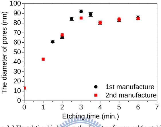
different etching time... - 53 -
Figure 3-2 FESEM images of the one-step aao thin film with different etching time. The images in left column are the top view of these thin films. The images in the right column are the side view of these thin films... - 54 -
Figure 3-2 (cont’d) FESEM images of the one-step aao thin film with different etching time. The images in left column are the top view of these thin films. The images in the right column are the side view of these thin films... - 55 -
Figure 3-2 (cont’d) FESEM images of the one-step aao thin film with different etching time. The images in left column are the top view of these thin films. The images in the right column are the side view of these thin films... - 56 -
Figure 3-6 Polarizing microscopic images of the liquid crystal cells with the etched aao thin film as the alignment layer... - 59 -
Figure 3-10 Scheme of the possible alignment mechanism... - 63 -
Figure 4-1 Spectrum of electromagnetic wave. ... - 87 -
Figure 4-2 Structure of the photoconductive dipole antenna... - 87 -
Figure 4-3 The calculated photocurrent in the emitting photoconductive antenna and the amplitude of the thz field versus time. The temporal pulse shape of the ultrashort pulse is shown as a dotted line... - 88 -
Figure 4-4 Scheme of the terahertz time-domain spectroscopy system. ... - 88 -
Figure 4-5 THz field signal measured by using thz-tds system. The red line is the atmosphere signal (r.h.~65%). The black line is the atmosphere signal with n2 purged (r.h.~3%)... - 89 -
Figure 4-6 Power spectrum of the thz signal in frequency domain. The red line is the atmosphere signal (r.h.~65%). The black line is the atmosphere signal with n2 purged (r.h.~3%)... - 89 -
Figure 4-8 Scheme of the thz wave pathway near the sample. (a) the thz wave pass through a cell with two substrates. (b) the thz wave pass through only two substrates... - 91 -
Figure 4-9 Spectrum of the water vapor absorption peak in thz region. The upper graph is the power spectrum (black line: r.h.~3%, red line: r.h.~65%). The middle and lower graph is the transmittance and the phase difference by using the n2 purged spectrum as a reference, respectively. The black line in the middle graph is the water vapor absorbance spectrum in ref. [12]. ... - 92 -
Figure 4-11 Optical constants of 3 mm fused silica substrate in thz region. The solid circles are the data in ref. [13]. The dashed line is the date in ref. [14]... - 94 -
Figure 4-13 Relationship between the refractive index and the porosity. ... - 96 -
Figure 4-14 Configuration of the FLC cell and its geometry with respect to the incident terahertz wave ... - 97 -
Figure 4-15 The thz-band real extraordinary and ordinary indices of refraction of the FLC in the SmA* phase (67.9 °C) and SmC* phase (58.1°C). ... - 97 - Figure 4-16 Frequency dependence of the thz-band extraordinary and ordinary
absorption coefficients of the FLC in the SmA* phase (67.9°C). To compare, both real and imaginary indices of refraction are also shown. The dashed lines indicate possible positions of the absorption bands. ... - 98 - Figure 4-17 Frequency dependence of the THz-band extraordinary and ordinary
absorption coefficients of the FLC in the SmC* phase (58.1°C). To compare, both real and imaginary indices of refraction are also shown. The dashed line indicates possible position of the absorption band. ... - 99 - Figure 5-1 Chemical formula and the chemical structure of PDMS (from wiki). - 109 - Figure 5-2 Schematic process of the thermo-imprinting technology and the
UV-imprinting technology ... - 110 - Figure 5-3 AFM report of the imprinted PDMS substrate with 5 μm groove. (a) the
first imprinted groove pdms substrate, (b) the second imprinted groove pdms substrate. ... - 111 - Figure 5-4 The polarizing images of the liquid crystal cell with the grooved PDMS
substrates as the alignment substrate in a pair of cross polarizers. The power of O2 plasma is 70w and 114w. The treating time is 0.1 min. and 0.3 min. ... - 112 -
Figure 5-4 (cont’d) The polarizing images of the liquid crystal cell with the grooved PDMS substrates as the alignment substrate in a pair of cross polarizers. The power of O2 plasma is 70w and 114w. The treating time is 0.1 min. and 0.3 min.
... - 113 - Figure 5-4 (cont’d) The polarizing images of the liquid crystal cell with the grooved
PDMS substrates as the alignment substrate in a pair of cross polarizers. The power of O2 plasma is 70w and 114w. The treating time is 0.1 min. and 0.3 min.
... - 114 - Figure 6-1 The setup of this new method. The incident light is monochromatic. - 127 - Figure 6-2 Photographs of the wedged samples with different spacers at the wider end:
(a) 50 μm (b) 75 μm (c) 250 μm. P: polarizer axis, A: analyzer axis, and R: rubbing direction... - 127 - Figure 6-3 Transmittance simulation of the wedge cell with ψ0=45°... - 128 -
Figure 6-4 Transmittance simulation of the wedge cell with ψ0=3°... - 128 -
Figure 6-5 Analysis of error of anchoring strength, ΔA/A, versus error in birefringence Δn. Solid curves are calculated using the true pitch value. Dashed curves are calculated using the pitch value measured with the presented method. ... - 129 - Figure 6-6 Solid curves plot the error ratio Δθ/θ versus A. Dashed lines plot ΔP/P
Figure 6-7 Relationships among twist angle θ, θcotθ and anchoring strength... - 130 - Figure 6-8 Relationship between x=(θ/d)/(2π/P-θ/d) and anchoring strength... - 130 -
Figure 7-1 FESEM images of the AAO thin film on the ito glass substrate. (a) the side view, (b) the top view. ... - 135 - Figure 7-2 The on-state and off-state of the prototypical cell with the AAO-ITO thin
films as the alignment layers... - 136 - Figure A-1 Scheme of the anodizing system. ... - 145 - Figure A-2 Processes of forming anodic aluminum oxide films: (a) the one-step
process, and (b) the two-step process. ... - 146 - Figure A-3 FESEM images of the AAO thin film. (top view) (a) one-step AAO thin
film, (b) two-step AAO thin film... - 147 - Figure A-4 FESEM images of the AAO thin film. (side view) (a) one-step AAO thin
film, (b) two-step AAO thin film... - 147 - Figure A-5 Scheme of the elementary process involved in the porous AAO thin film
growth. ... - 148 - Figure B-1 Scheme of the deviated angle in the azimuthal and polar direction. .. - 154 - Figure B-2 Scheme of the liquid crystal distribution in a vertically aligned cell. - 154 - Figure C-1 Screenshot is shown the threshold function and the dialog window.. - 159 - Figure C-2 (a) the AAO SEM image after threshold selection (b) the AAO SEM
image after 10 times smooth... - 159 - Figure C-3 Dialog window of analyze particles. ... - 160 - Figure C-4 Different layout after analyzing particles.(the documents of ImageJ)- 160 - Figure C-5 Actual AAO SEM image analysis by using the outlines layout... - 161 -
List of Tables
Table 2-1 The total charge of the one-step anodizing process for different anodizing voltage... - 31 - Table 2-2 The total charge of the two-step anodizing process for different anodizing
voltage... - 31 - Table 3-1 The diameter of pores, the thickness of the etched AAO thin film, and the
aspect ratio with different etching time. ... - 52 - Table 4-1 Characteristics of photoconductive substrates... - 86 - Table 4-2 Water vapor absorption lines in thz region. The data shown in the left
column are from reference [11]. The data shown in the middle column are from reference [12]. The data shown in the right column are read out from figure 4-9. ... - 86 - Table 5-1 Contact angles of water on the grooved PDMS substrate before O2 plasma
treatment. ... - 108 - Table 5-2 Contact angles of water on the grooved PDMS substrate after O2 plasma
Chapter 1
Introduction
1.1 Liquid crystals
In the fundamental physics, such as high school physics or university physics, everyone has been taught that substance only exists three phases: solid, liquid, and gas. In particular, some organic materials do not show a single transition from solid phase to liquid phase. The mechanical and the symmetry properties of these new phases are intermediate between those of a liquid and those of a solid. Therefore, these new phases are often called “liquid crystals”. Liquid crystals can be divided into three different phase depending on the physical properties, such as thermotropic, lyotropic and metallotropic phases. The thermotropic liquid crystals exhibit a phase transition into the liquid crystal phase as temperature is changed. The phase transition of the lyotropic liquid crystals depends on both temperature and concentration of the liquid crystal molecules in a solvent, such as water. Most of the thermotropic and lyotropic liquid crystals consist of organic molecules. The metallotropic liquid crystals are composed of not only organic but also inorganic molecules. The liquid crystal transition of the metallotropic liquid crystal depends not only on temperature and concentration, but also on the inorganic-organic composition ratio.
According to the different arrangement of liquid crystal molecules, the thermotropic liquid crystals can also be distinguished into three different types: nematic, smectic, and cholesteric. Figure 1-1 shows the schematic of liquid crystal alignment in these three different phases. In the nematic phase, the liquid crystal molecules have no positional order, but have long-range orientational order. Therefore, the center of mass positions of the liquid crystal molecules are randomly distributed as a liquid, but they all point to the same direction. The smectic phase usually forms several well-defined layers, and is usually found at
lower temperature than the nematic phase. There are many different smectic phases. All of these smectic phases are characterized by different types and degrees of positional and orientational order. [1] The cholesteric phase, also called the chiral nematic phase, exhibits chirality or handedness. The first cholesteric phase was observed for cholesterol derivatives. Most of the liquid crystals which have the cholesteric phase are chiral molecules that are without inversion symmetry.[1] In this work, nematic liquid crystal is used in most of our experiment.
The well arrangement of the anisotropic rodlike molecules directly results in the anisotropy of mechanical, electric, magnetic, and optical properties. In the liquid crystal displays applications, the most important anisotropic properties are the optical and electric properties. As a result of the orientational ordering of the nematic liquid crystals molecules, the nematic liquid crystals are uniaxial with the symmetric axis parallel to the axes of the molecules, called the director nˆ. Because of the uniaxial symmetry, the dielectric constants are different in value parallel to (ε//) and perpendicular to (ε⊥) the director. The dielectric anisotropy is defined as
⊥
− =
Δε ε// ε . (1-1)
The sign and magnitude of the dielectric anisotropy are both important in liquid crystal displays application by using the various electric fields to control the liquid crystal displays. Usually, the macroscopic dielectric constant is often proportional to the molecular polarizability. For the rodlike molecules, such as the nematic liquid crystal molecules, the longitudinal polarizability (parallel to molecular axis) is often larger than the transverse polarizability (perpendicular to axis). Most of the rodlike molecules have induced dipole in the applied electric field. Because the induced dipole is parallel to the director, the dielectric anisotropy is positive, Δε >0, and ε// >ε⊥. 4`-n-pentyl-4-cyanobiphenyl (5CB)
polar liquid crystal compounds have the permanent dipole moment. Depending on the angle between the permanent dipole moment and the molecular axis, the additional contributions increase or decrease the dielectric constant. The increase or decrease of the dielectric anisotropy Δ results in the negative value of the ε dielectric anisotropy, called the negative liquid crystals (e.g., p-Methoxybenzylidene-p`-n-butylaniline, MBBA).[1] The dielectric anisotropy also depends on the temperature. ε// and ε⊥ approaches to each other near the clearing point Tc. Beyond the clearing point, the dielectric constant becomes the mean dielectric constant
3 2 // + ⊥ =ε ε ε . (1-2)
Figure 1-2 shows the characteristic of the dielectric constants for 5CB.[3] Here, ε is calculated from the measured values of ε//, ε⊥ and Equation (1-2). The dashed line denotes the extrapolated value of the dielectric anisotropy in isotropic state, εiso.[4]
On the other hand, the nematic liquid crystals also show the anisotropic properties in optical region, called the optical anisotropy. Without proper boundaries or the applied field (magnetic field or electric field), the directors and the refractive index of liquid crystal molecules are random, and the incident light is scattered. Because of the discontinuity of the refractive indices at the domain boundaries, the nematic liquid crystals usually appear as a milky fluid. A nematic liquid crystal cell with the proper treated alignment layers exhibits the optical properties as an uniaxial crystal with two principal refractive indices no and ne. The ordinary refractive index no is for light with the polarization of the electric field perpendicular to the director. The extraordinary refractive index ne is for light with the polarization of the electric field parallel to the director. The optical anisotropy, also called the birefringence, is defined as
o
e n
n n= −
Δ . (1-3)
If Δn>0⇒ne >no, the liquid crystal has positive birefringence, whereas if
o
e n
n n< ⇒ <
Δ 0 , the liquid crystal has negative birefringence. For most liquid
crystals, the ordinary refractive index n is around 1.5, and the birefringence is o
from 0.05 to 0.45. This optical anisotropy plays an essential role in changing the polarization state of light in liquid crystals. Figure 1-3 shows the characteristic of
e
n , n and o Δn of 5CB.[5] It clearly shows the similar behavior as the dielectric constants. It is because that the refractive index is also related to the molecular polarizability at optical frequencies and the anisotropic molecular structure.
1.2 Liquid crystal display applications
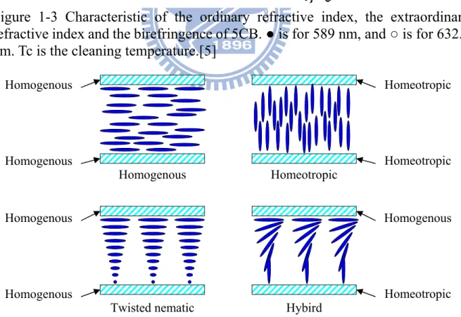
In liquid crystal display applications, the liquid crystal molecules are usually sandwiched between two substrates coating with the alignment layers. Depending on different alignment layers, the liquid crystal molecules orient homogenously or homeotropically. Figure 1-4 shows the typical orientations of liquid crystal molecules in different liquid crystal displays. The liquid crystal molecules align parallel to the substrates in the homogenous cell and perpendicular to the substrates in the homeotropic cell. For the twist nematic cell, the directors of the liquid crystal molecules near two substrates are different, one with 90° respect to another. In the hybrid cell, the liquid crystal molecules on one substrate have homogenous alignment and those on the other substrate have homeotropic alignment. The homogenous alignment can be obtained by rubbing polyimide films, photoalignment method and using the microgrooved substrates. The homeotropic alignment can be obtained by coating the substrate with hydrophobic films such as silane compounds or the ferromagnetic film. The SiO oblique evaporation method can give any of the homogenous, homeotropic and tilted alignments by controlling the evaporation angle. All of these alignment methods
will be introduced in the following sections.
1.3 Rubbing alignment method
In the 70s, the early stages of liquid crystal displays production, only the rubbing method has been adopted for alignment technologies. The rubbing alignment method is a simple, convenient, and low-cost method. A typical rubbing machine includes a rolling cylinder covered by the rubbing cloth and a substrate holding stage. The cylinder rotates 100-800 rpm, and can be controlled to move up and down relative to the substrate stage. The glass substrates with alignment layers are fixed to the stage by using air suction. By rotating the angle of the substrate on the stage, the rubbing direction on the alignment layer can be controlled. The rotating cylinder moves down to the substrate and applies pressure to the substrate. Then, the substrate stage moves forward with a constant velocity. After the entire area is rubbed, the cylinder moves away and the substrate stage returns to the initial position.[6]
However, when the production of the thin film transistors liquid crystal displays (TFT-LCDs) started in the 80s, defects of the rubbing method were highlighted. In the rubbing method, the surface of polyimide layers is rubbed with a cloth. Several problems were pointed out: (a) the TFTs are destroyed by the static electricity caused by the friction between the surfaces of the cloth and the polyimide layers, (b) the direct contact between the surfaces and the cloth causes defects and stains on the surface of alignment layer, and (c) the clean room is polluted by fiber from the cloth.
1.4 Photoalignment method
The photoalignment method is a non-contact method for liquid crystal alignment. The non-contact method can prevent a lot of problems which are produced from the rubbing process, such as the static electricity and dust. The
most common photoalignment method is the alignment method by generating the anisotropic distribution of the molecules of the alignment materials using the polarized light irradiated on the alignment layer. In 1991, W. M. Gibbons et al. presented the photoalignment method that the liquid crystal molecules were aligned by using the polarized laser light in visible range.[7] The photochemical reactions of the photoalignment method can be categorized as photoisomerization, photodimerization, photodecomposition, photocrosslinking and a combination of photodecomposition and photolinking. By using the conformational change between cisoid-type and transoid-type azobenzene functional units, the photoisomerization reaction can control the liquid crystal alignment.[8] It is a reversible change between homeotropic and homogenous alignment by controlling the wavelength or the polarization of the irradiated light.[9]
Polyvinyl cinnamate (PVCi) is a well-known material that aligns liquid crystal molecules by photodimerization process.[10][11] PVCi absorb the energy of the irradiated linear polarization light which polarization axis is parallel to the double bonds of PVCi. The double bonds are scissored and then two of the scissored bonds are reconnected and dimerized. The alignment direction of the liquid crystal molecules is perpendicular to the polarization of the light for PVCi.
The photodecomposition reaction has been applied to a various photosensitive materials compared with the other two methods, photoisomerization and photodimerization. Polyimide has been used as a photodecomposition material. The anisotropic photodecomposition of polyimide by irradiating the polarized UV light changes the anisotropic molecular length distribution. The distribution can control the alignment of liquid crystal molecules.
By irradiating the UV light, the crosslinking process connects one molecule to another molecule and generates a new structure. This new structure can be used to align the liquid crystal molecules. Some of photodecomposition material not only break bonds and create new structures, but also connect these structures and
become a new anisotropic alignment structure. This process is called the Hybird method (photocomposition and photocrosslinking). However, the photoalignment mechanisms in some material are not clearly understood because the photochemical reactions are different in each photoalignment material.
1.5 Ion beam bombardment method
The ion beam bombardment method is another novel non-contact alignment method. It is developed only in the past decade. In 1998, an IBM research group invented that the liquid crystal molecules can be aligned on the polyimide or diamond-like carbon (DLC) alignment layer which is bombarded by a low energy and neutral argon ion beam.[12][13] Recently, Stöhr et al. discovered that the ion beam bombardment changes the carbon double or triple bonds. This anisotropic change introduces the surface orientational anisotropy.[14] Any amorphous layer with directional sp2 and sp bonds, such as SiNx, SiC, SiO2, SnO2, ZnTiO2 and
InTiO2, can align the liquid crystal.
During the past few years, the most remarkable research about the ion beam bombardment is that the homeotropic alignments can be obtained by using fluorinated DLC thin films as the alignment layer. The pretilt angle can also be controlled by the different parameters of the ion beam and the concentration of fluorine doped in DLC thin films.[15] On the other hand, by using the ion beam with different energies, both homeotropic and homogenous alignment can be applied on the same organic alignment layer.[16][17]
Recently, our group has developed a novel alignment method by using ion beam bombardment on different alignment materials. We have demonstrated that both homeotropic and homogenous alignments can be obtained with the same ion beam apparatus and polyimide by varying the ion beam energy or the bombarding time.[18] Another alignment method is by using a one-step, ion beam bombardment of the glass substrates without polyimide layer. The homeotropic
alignment is achieved due to orientation of the diamagnetic nematogenic molecules by the magnetic field from the γ-Fe2O3 ferrimagnetic thin films created
on the substrates by ion beam bombardment. This is a simple, noncontact, and reliable alignment method for liquid crystal devices.[19][20]
1.6 Chemical treatment method
After chemically treating the substrates, the substrates can provide the homeotropic or homogenous alignment. The surface active agents, such as silicone compounds, are used to obtain homeotropic alignment. The silicon compounds react with the substrate surface and polymerize to form polysiloxane structures near the surface. N, N-dimethyl-N-octadecyl-3-amino-propyl -trimeth oxysilyl chloride (DMOAP) is usually used to homeotropic alignment. The surface treatments with DMOAP are carried out by dipping the substrate into a 1% aqueous solution of the silane compounds, DMOAP. There are other methods to treat the surface of substrate. By exposing the substrate to the vapor of pure silane compounds or spreading silane compounds on the surface, the surface can be treated and become the homeotropic alignment surface. In 1973, F. J. Kahn investigated the alignment properties of N-methyl-3-amino-propyl -trimethoxy-silane (MAP) and DMOAP.[32] Figure 1-5 shows the names and the chemical formulas of DMOAP and MAP. The schemes also represent the orientations of their components propyl (CH2)3 and octadecyl (C18H37). For
DMAOP with long alkyl chains, the propyl chain attaches on the substrate surface and the octadecyl chain orients out of plane. The liquid crystal molecules can align along the octadecyl chain. It is the most used vertical alignment method.
1.7 Other alignment method
Besides the rubbing method, the photoalignment method and the ion beam bombardment method, there are some other alignment method, such as the
oblique evaporation method and the microgroove surface method. SiO is the most common material used in the oblique evaporation method. After the oblique evaporation process, the micro SiO columnar structure is formed on the substrate surface. The columnar angle is dependent on the evaporation angle and changes in the nematic alignment direction and the pretilt angle.[21]
For the microgroove surface method, our group has demonstrated that the liquid crystal molecules can be aligned on the U-shaped grooves surface formed on the substrate with variable depths and spacing by using the reactive ion etching (RIE) method. [22] The periods of grooves were varied from 2 μm to 9 μm with three different depths by changing the etching time in the RIE process. The anchoring strengths are within the range of 1×10⁻⁸ ~ 2×10⁻⁶ J/m2. It can be increased by more than an order of magnitude by varying the groove depth and period.
1.8 Mechanism of liquid crystal alignment
As what we have discussed, the alignment layer is necessary for the liquid crystal displays application to align the liquid crystal molecules without any applied field. The major mechanisms for the alignment of liquid crystals on the alignment layer, such as the rubbed polymer film, are the micro-morphology of the alignment surface and the interaction force between the liquid crystal molecules and the alignment molecules. The mechanism of the micro-morphology was suggested by D. W. Berreman.[23] He mentioned that the liquid crystal molecules prefer to align parallel to the induced grooves to reduce the total surface free energy. Here we review his calculations as following. The groove surface can be approximately described by a sinusoidal wave
( )
qx Az ≈ sin where A is the depth of the groove on the surface and λ =2π q is the frequency of the groove. The anchoring energy can be calculated by using the elastic energy based on the Oseen-Frank elastic continuum theory.[24][25] The
azimuthal anchoring energy Wφ calculated as W K Aq 2q 11( ) 4 1 = φ . Here, K11 is a
splay elastic constant of the liquid crystal.
On the other hand, J. M. Geary et al. suggested that liquid crystal molecules are anchored to buffed polymer chains of the polymer surfaces. The alignment of the liquid crystal molecules follows in an epitaxial manner.[26] The reorientation of polymers which gives the anisotropic characteristics caused by rubbing have been confirmed by optical retardation, IR absorption spectra and second harmonic generation. In view of problems mentioned above, studies on both the mechanism of the rubbing process and the development of other methods for liquid crystalline alignment have been carried out. Thus, novel alignment technologies are required that not only achieve increase in production yields, but also offer additional advantages, such as the convenience of multi-domain alignment.
1.9 Overview of this work
In this work, we develop two novel alignment methods based on the micro-morphology mechanism. The first alignment method is a novel vertical alignment method which is by using the porous anodic aluminum oxide (AAO) thin film as the alignment layer. The porous AAO thin film is formatted by anodizing the aluminum thin film in the acidic electrolyte. The detailed manufacture process is described in Appendix A. The morphology of porous AAO thin film surface is a nanopores array. It offers the liquid crystal molecules an excellent vertical alignment layer. The second alignment method is a homogenous alignment method on the grooving surface by using the nanoimprinting method.
In Chapter 2 and Chapter 3, we demonstrate the strong vertical alignment of liquid crystal on porous AAO thin film and also discuss the polar anchoring strength of the AAO thin film with different pores sizes and different aspect ratio, respectively. In detail, the measuring method of the polar anchoring strength by
using the magnetic field method is described in Appendix B.
In the past few years, our group has studied the optical constants of the liquid crystals in terahertz region[27][28] and developed several terahertz devices, such as the electrically controlled quarter and full wave plate[29][30] and the magnetically controlled phase shifter[31], based on the liquid crystal devices. In order to apply the AAO thin film as an alignment layer in terahertz region, we investigate the optical properties of the AAO thin film by using the terahertz time-domain spectroscopy in Chapter 3.
In Chapter 5, we demonstrate the preliminary work about the homogenous alignment on the flexible polydimethylsiloxane (PDMS) substrate. Here we use the glass substrates with the U-shaped groove as the imprinting mode. By using the nanoimprinting technology, the U-shaped groove can be imprinted on PDMS substrate. After O2 plasma treatment, the nematic liquid crystal can be aligned homogenously on the PDMS surface and parallel to the groove direction.
In order to investigate the homogenous alignment ability in the previous chapter, the azimuthal anchoring strength is a physical parameter to indicating the ability of the alignment layer. In Chapter 6, we develop a novel method to measure the pitch of the chiral nematic liquid crystal. By using this modified pitch to calculate the azimuthal anchoring strength, the error of the azimuthal anchoring strength can be reduced and become less than 1%.
Finally, in Chapter 7, we summarize all remarkable conclusions about each novel alignment method discussed in this thesis. Furthermore, we provide some interesting research topics for future work.
References
[1] P. G. de Gennes, and J. Prost, “The Physics of Liquid Crystals,” Oxford University Press, ISBN 0-19-852024-7 (1994).
[2] L. M. Blinov, and V. G. Chigrinov, “Electrooptic Effects in Liquid Crystal Materials,” Springer-Verlag New York, ISBN 0-387-94030-8 (1994).
[3] S. Chandrasekhar, “Liquid Crystals,” 2nd Ed., Cambridge University Press, ISBN 0-521-42741-X (1992).
[4] B. R. Ratina, and R. Shashidhar, “Dielectric properties of 4`-n-alkyl-4-cyanobiphenyls in their nematic phases,” Pramana 6, 278 (1976).
[5] R. G. Horn, “Refractive indices and order parameters of two liquid crystals,” J. Phys. France 39, 105 (1978).
[6] T. Uchida, M. Hirano, and H. Sakai, “Director orientation of a ferroelectric liquid crystal on substrates with rubbing treatment: The effect of surface anchoring strength,” Liquid Crystals 5, 1127 (1989).
[7] W. M. Gibbons, P. J. Shannon, S. T. Sun, and B. J. Swetlin, “Surface-mediated alignment of nematic liquid crystals with polarized laser light,” Nature 351, 49 (1991).
[8] Y. Kawanishi, T. Tamaki, M. Sakyragi, T. Seki, Y. Suzuki, and K. Ichimura, “Photochemical induction and modulation of nematic homogenous alignment by the polarization photochromism of surface azobenzenes,” Langmuir 8, 2601 (1992).
[9] K. Ichimura, Y. Suzuki, T. Seki, A. Hosoki, and K. Aoki, “Reversible change in alignment mode of nematic liquid crystals regulated photochemically by command surfaces modified with an azobenzene monolayer,” Langmuir 4, 1214 (1988).
parallel alignment of liquid crystals by linearly polymerized photopolymers,” Jpn. J. Appl. Phys. 31, 2155 (1992).
[11] Y. Iimura, T. Saitoh, S. Kobayashi, and T. Hashimoto, “Liquid crystal alignment on photopolymer surfaces exposed by linearly polarized UV light,” J. Photopolymer Sci. and Tech. 8, 257 (1995).
[12] P. Chaudhari, J. Lacey, S. C. Alan Lien, and J. L. Speidell, “Atomic beam alignment of liquid crystals,” Jpn. J. Appl. Phys. 37, L55 (1998).
[13] P. Chaudhari, J. Lacey et al., “Atomic-beam alignment of inorganic materials for liquid-crystal displays,” Nature 411, 56 (2001).
[14] J. Stöhr, M. G. Samant, J. Lüning, A. C. Callegari, P. Chaudhari, J. P. Doyle, J. A. Lacey, S. A. Lien, S. Purushothaman, and J. L. Speidell, “Liquid crystal alignment on carbonaceous surfaces with orientational order,” Science 292, 2299 (2001).
[15] H. J. Ahn, S. J. Rho, K. C. Kim, J. B. Kim, B. H. Hwang, C. J. Park, and H. K. Baik, “Ion-beam induced liquid crystal alignment on diamond-like carbon and fluorinated diamond-like carbon thin films,” Jpn. J. Appl. Phys.
44, 4092 (2005).
[16] J. S. Gwag, K. H. Park, J. L. Lee, J. C. Kim, and T. H. Yoon, “Two-domain hybrid-aligned nematic cell fabricated by ion beam treatment of vertical alignment layer,” Jpn. J. Appl. Phys. 44, 1875 (2005).
[17] S. H. Lee, K. H. Park, J. S. Gwag, T. H. Yoon, and J. C. Kim, “A multimode-type transflective liquid crystal display using the hybrid-aligned nematic and parallel-rubbed vertically aligned modes,” Jpn. J. Appl. Phys.
42, 5127 (2003).
[18] H. Y. Wu, T. T. Tang, C. C.Wang, R. P. Pan, S. J. Chang, and J. C. Hwang, “Controllable alignment modes of nematic liquid crystals on argon ion beam bombarded polyimide films,” Mol. Cryst. Liq. Cryst. 475, 45 (2007).
[19] H. Y. Wu, and R. P. Pan, “Liquid crystal surface alignments by using ion beam sputtered magnetic thin films,” Appl. Phys. Lett. 91, 074102 (2007).
[20] R. P. Pan, H. Y. Wu, and C. F. Hsieh, “Liquid crystal surface alignment by using films composed of magnetic nanoparticles,” Proc. SPIE 6911, 691104 (2008).
[21] J. L. Janning, “Thin film surface orientation for liquid crystals,” Appl. Phys. Lett. 21, 173 (1972).
[22] Y. F. Lin, M. C. Tsou, and R. P. Pan, “Alignment of liquid crystals by ion etched grooved glass surfaces,” Chinese J. Phys. 43, 1066 (2005).
[23] D. W. Berreman, “Solid surface shape and the alignment of an adjacent nematic liquid crystal,” Phys. Rev. Lett. 28, 1683 (1972).
[24] C. W. Oseen, “The theory of liquid crystals,” Trans. Faraday Soc. 29, 883 (1933).
[25] F. C. Frank, “I. Liquid crystals. On the theory of liquid crystals,” Discuss. Faraday Soc. 25, 19 (1958).
[26] J. M. Geary, J. W. Goodby, A. R. Kmetz, and J. S. Patel, “The mechanism of polymer alignment of liquid-crystal materials,” J. Appl. Phys. 62, 4100 (1987).
[27] T. R. Tsai, C. Y. Chen, C. L. Pan, R. P. Pan, and X. C. Zhang, “Terahertz Time-Domain Spectroscopy Studies of the Optical Constants of the Nematic Liquid Crystal 5CB,” Appl. Opt. 42, 2372 (2003).
[28] R. P. Pan, T. R. Tsai, C. Y. Chen, and C. L. Pan, “Optical constants of two typical liquid crystals 5CB and PCH5 in the THz frequency range”, J. Bio. Phys. 29, 335 (2003).
[29] C. F. Hsieh, R. P. Pan, T. T. Tang, H. L. Chen, and C. L. Pan, “Voltage-controlled liquid-crystal terahertz phase shifter and quarter-wave plate,” Opt. Lett. 31, 1112 (2006).
[30] H. Y. Wu, C. F. Hsieh, T. T. Tang, R. P. Pan, and C. L. Pan, “Electrically tunable room-temperature 2π liquid crystal terahertz phase shifter”, IEEE Phtonics Tech. Lett. 18, 1488 (2006).
terahertz phase shifter based on magnetically controlled birefringence in liquid crystals,” Appl. Phys. Lett. 83, 4497 (2003).
[32] F. J. Kahn, “Orientation of liquid crystals by surface coupling agents,” Appl. Phys. Lett. 22, 386 (1973).
Figures
Figure 1-1 Scheme of different type of liquid crystal.
Figure 1-2 Characteristic of the dielectric constant of 5CB. [3]
Figure 1-3 Characteristic of the ordinary refractive index, the extraordinary refractive index and the birefringence of 5CB. ● is for 589 nm, and ○ is for 632.8 nm. Tc is the cleaning temperature.[5]
Figure 1-4 Typical orientations of liquid crystal molecules in different liquid crystal displays.
Homogenous Homeotropic
Twisted nematic Hybird
Homogenous Homogenous Homeotropic Homeotropic Homogenous Homogenous Homogenous Homeotropic
Figure 1-5 Chemical formulas of DMOAP and MAP and the surfaces which result from their application to a substrate.[32]
Chapter 2
Strong vertical alignment of liquid crystal
on anodic aluminum oxide film
with different pore size
2.1 Overview
Anodic Alumina Oxide (AAO) is an inorganic and porous material. It is almost transparent and colorless in visible region. Because of these properties, AAO film is a good candidate as the alignment layer of liquid crystal displays.
Appendix A.2 shows how to manufacture the porous AAO thin film. The
mechanism of AAO formation is also discussed in Appendix A.4. Recently, T. Maeda and K. Hiroshima had demonstrated the vertical alignment of liquid crystal molecules on AAO films. [1][2] In their work, the depth and the diameter of the nanopores in the AAO film are 100-150nm and 5-20nm, respectively. The measured pretilt angle and the observed conoscopic pattern of the liquid crystal cells indicate that the liquid crystal molecules are aligned vertically on AAO films. They also showed that the pretilt angle can be changed by anodizing the pre-rubbing aluminum film. In this work, we use both one-step and two-step process to produce non-uniform and uniform porous AAO thin film, respectively. By using different anodizing voltages, we can control the pore sizes of the AAO films. We examined the relationship between the polar anchoring strength and the anodizing voltage. All these different AAO films are good vertical alignment layers. It is shown, however, that the anchoring strength depends on anodizing condition. This is due to the voltage-dependent pore sizes of the AAO films.
2.2 Experimental procedures
foil in acid electrolytes. By using one-step process or two-step process, it is easy to form crack-like or hexagonal porous AAO structure. The pore sizes are controllable by varying the anodizing voltage. For the two-step process, the thickness of AAO thin film can be controlled by changing the anodizing time of the first step. The remaining curved aluminum thin film can form the uniform porous AAO thin film. The more detail manufacture description is shown in
Appendix A.2.
By using the field emission scanning electron microscope (FESEM: HITACHI S-4700i), we can observe the morphology and the nanostructure of the porous AAO thin film. All AAO thin films are evaporated thin platinum or gold layer to reduce charging effects. The thickness of AAO thin film can be measured by examining the cross-view of the AAO FESEM image. By using the image processing program, ImageJ, we can analysis the FESEM image to determine the average pore size, the average AAO wall area, and the density of pores. The software introduction and the analysis algorithm of ImageJ are shown in Appendix C.
In order to use the AAO thin film as the alignment layer, the transmittance of AAO thin films in visible region are very important. The transmittance of AAO thin films are taken by using a UV-Visible spectrometer (Oceanoptics, model ISS-UV-VIS and USB2000) with air as the reference.
Finally, we need to investigate the alignment characterization of the AAO thin film. The investigative cell is made by putting together a pair of glass substrates with the AAO film face to face. The nematic liquid crystal, 5CB (Merck) was filled into the cell in the isotropic phase (above 36°C). The thickness of liquid crystal layers is 23 μm. The liquid crystal alignment in the cell is examined with a polarizing microscope. The cell is put between a pair of crossed polarizers. By using the polarizing microscope, we can examine the transmitted image and the conoscopic image. The conoscopy is a useful optical method to analyze the alignment of the uniaxial crystals by observing the interference
image.[3]
By applying the magnetic field on the vertical alignment cell, the polar anchoring strength can be determined from the transmittance, which is a function of applied magnetic field above the threshold magnetic field. The polar anchoring strength characterizes the surface energy ability out of the substrate plane. The theory and analysis method of the polar anchoring strength are discussed in Appendix B.
2.3 Results and discussions
2.3.1 Anodizing current characterization
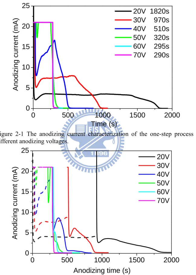
By using the function of the power supply (Keithley Instruments Inc. Model 2410 General-Purpose SourceMeter), we can record the anodizing current during the anodizing process. For the anodizing current characterization analysis, the thickness of the aluminum thin film is 500 nm. The anodizing current characterization is shown in Figure 2-1 and Figure 2-2 for one-step and two-step process, respectively. For both one-step and two-step process, the anodizing process with lower anodizing voltage has lower anodizing current and longer anodizing time. According to the manual of 2410 SourceMeter, the maximum power is 22W. The range of operation is 21V at 1.05A or 1100V at 21mA.[4] Because the range of operation is 21V for 20V, the capability of anodizing current can be 1.05A. When the anodizing voltage is larger than 20V, the range of operation is 1100V, the capability of anodizing current can only be 21mA. In Figure 2-1 and Figure 2-2, it is obviously that the anodizing current is saturated at 21mA for V≥50V. In Figure 2-2, the dash and solid line are the anodizing current characterization of the first and second step process of two-step process, respectively.
For more investigations, we can integrate the anodizing current by the anodizing time. The integrated result is the total charge of the anodizing process.
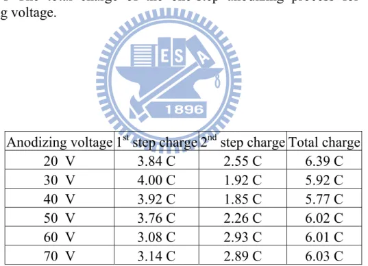
Table 2-1 shows the total charge of the one-step anodizing process for different anodizing voltage. It clearly shows the total charge is around 6 Coulomb regardless the anodizing voltage. According to the mechanism, the total charge is proportional to the thickness and the anodized area of the aluminum thin film. Table 2-2 shows the charge of first step and second step in the two-step process for different anodizing voltage. The total charges are also around 6 Coulomb for different anodizing voltage, even the first step or the second step is different anodizing duration.
2.3.2 Morphology of the anodic aluminum oxide surface
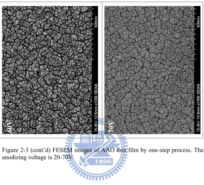
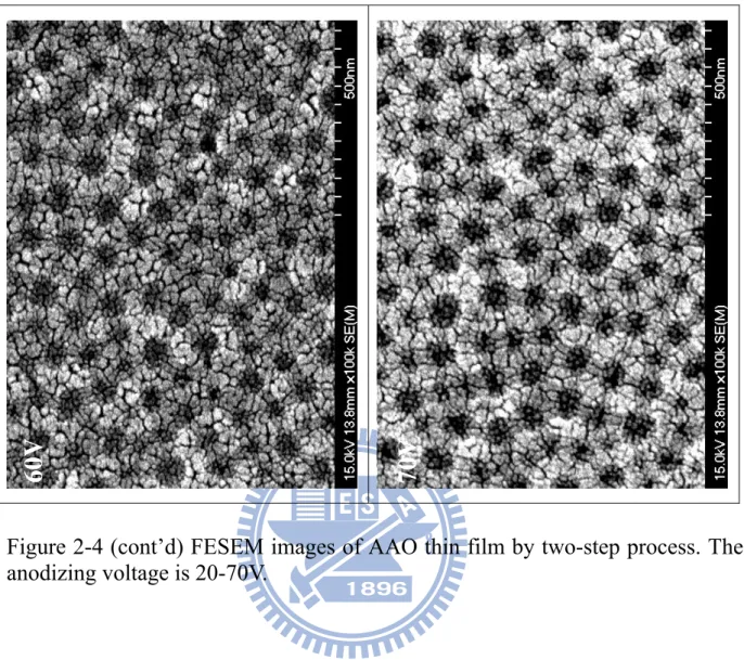
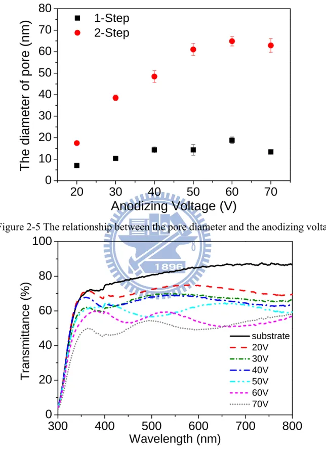
Figure 2-3 shows the FESEM image of the AAO film formed by using the one-step process. There were only fine crack-like structures connecting irregular small pores on the surface of the AAO film. When the anodized voltage was varied from 20 to 70V, the widths of the pores remained almost the same, about 5-15nm. By using the two-step process, the surface of the AAO film had regular pores as shown in Figure 2-4. These pores were self-assembled into hexagons. According to cross-sectional observation by the FESEM, the actual thicknesses of AAO films prepared by the one-step process were 415±15 nm, while those by the two-step process were 210±30nm. In Figure 2-5, we show the relationship between the diameter of pores and the anodizing voltage. The pore size is determined by measuring some pores in the SEM image directly. The data dots in Figure 2-5 are the average size of these pores and the error bars are the standard deviation of these pores.
The diameters of pores for the two-step process increased linearly from 15 to 50nm as the anodizing voltage was increased from 20V to 50V. For V > 50V, the diameter of pore was saturated at a value around 65nm. The saturated values for pore diameters were observed for both cases, nonetheless. According to the anodizing current characterizations, we note that the anodizing current was saturated at 21mA, the current limit of the power supply, when V > 50V. If the
anodizing current is saturated at the current limitation, the power supply will operate in constant current mode, and the anodizing voltage will be limited by the maximum current, 21mA for Model 2410, when V > 50V. In contrast, the diameters of pores for AAO prepared by the one-step process were small and did not exhibit apparent trend when the anodizing voltage was varied in this range.
2.3.3 Transmittance of the anodic aluminum oxide layer
Figure 2-6 shows the transmittance of the AAO films on the ITO glass substrate as a function of wavelength from 300 to 800 nm. The cut off wavelength at 350nm is due to absorption of the ITO glass substrate. For the AAO films anodized at a bias voltage from 20V to 40V, the transmittance is about 65% over this spectral range. In comparison, the transmittance of the substrates with the ITO thin film on the back side is around 80%. For AAO films anodized at a bias voltage from 50V to 70V, the transmittance reduces to about 55%. Ripples in the spectral transmittance for the AAO films, for which the thickness varies from 300 to 500 nm, are attributed to the interference effects of the films. The spectral transmittance of the substrate is relatively smooth, because the ITO-film is very thin, 50-100 nm in thickness. Our data showed that the AAO film is highly transparent in the visible region and is a very good candidate of alignment layer in LCD applications.
2.3.4 Alignment characterization
In this section, the alignment characterizations are investigated by using the liquid crystal cell. By putting together a pair of glass substrates with the AAO alignment layer face to face, the cell with cell gap of 23μm was made. The nematic liquid crystal, 5CB (Merck) was filled into the cell in the isotropic phase (above 36°C). The liquid crystal alignment in the cell was examined with a polarizing microscope in microscopic mode and conoscopic mode.
In Figure 2-7, we show the polarizing microscopic images of the liquid crystal cells with the AAO alignment thin film manufactured by using one-step process. The liquid crystal cells are observed in a pair of crossed polarizers. The micrographs are taken in two orientations of the cell, 45° with respect to each other. Regardless of the anodizing voltages, all of the liquid crystal cells show the dark state in both 0° and 45°. The dark state observed for both cases indicates that vertical alignment of liquid crystal was achieved. Figure 2-8 shows the polarizing microscopic images of the liquid crystal cells with the AAO alignment thin film manufactured by using two-step process. No matter what the anodizing voltage is, all of these images in Figure 2-8 are the dark state. That is mean all of the AAO thin film with two-step process are good vertical alignment.
Figure 2-9 shows the conoscopic image of the same liquid crystal cells with both one-step and two-step AAO alignment layers. It obviously shows that all conoscopic images are the cross texture. The cross texture also shows that the liquid crystal cell was vertically aligned.[3] Further, in order to confirm the vertical alignment, the pretilt angles of the liquid crystal cells were measured by using the crystal rotation method [5]. Figure 2-10 shows the pretilt angle of the liquid crystal cell with the AAO alignment layer. For all of these cells with anodizing voltage between 20 and 70V, the pretilt angles were between 89.5° and 90.0°. There is no significant difference between the samples prepared with one-step or two-step processes.
2.3.5 Polar anchoring strength analysis
According to the previous section, we already knew that the AAO thin film can vertically align nematic liquid crystal. In order to know the alignment ability of the AAO thin film and compare to the other traditional vertical alignment layer, N, N-dimethyl-N-octadecyl-3-amino-propyl-trimeth oxysilyl chloride (DMOAP) , we made a few liquid crystal cells with the same AAO alignment layer, and
measured the polar anchoring strength of these samples by using the magnetic field method [6]. The polar anchoring strengths of the liquid crystal cells are plotted versus the anodizing voltages from 20V to 60V as shown in Figure 2-10. The data dots in Figure 2-11 are the average anchoring strength, and the error is the standard deviation. For AAO films anodized at different voltages, the uniformities of the films are different. The error bars in anchoring strengths of AAO films with non-uniform pore sizes are larger than those of uniform ones.
As a reference, we have determined the polar anchoring strength of N,N-dimethyl-N-octadecyl-3-amino-propyl-trimeth oxysilyl chloride (DMOAP) to be 38±6×10⁻⁶ J/m2. Notably, AAO films prepared by these two methods show similar polar anchoring strengths, comparable but still somewhat smaller than that of the traditional vertical alignment film (DMOAP). Figure 2-11 also indicates clearly that the uniformity of the pore array is not a key parameter in effective alignment. In this sense, the one-step process for preparing AAO films is advantageous over the two-step process.
By the way, it is possible to reduce the anodizing voltage to 5 or 10 Volts. We expect such AAO films will have higher anchoring strength. Unfortunately, this will increase the anodizing time appreciably. According to our experimental data, the anodizing time for 20V is around 30 minutes. If we use lower anodizing voltage (5 or 10 V), it maybe take more than 1 hour.
According to Figure 2-5 and Figure 2-11, it is easy to show the relationship between the polar anchoring strength and pore diameter in Figure 2-12. Regardless of whether the AAO films were prepared by the one-step or two-step processes (the solid circles and squares, respectively), the polar anchoring strengths of AAO film with smaller pore diameters are stronger. The maximum polar anchoring strength for 5CB on the uniformly porous AAO film is 15×10-6 J/m2. Because 5CB is a rod-like nematic liquid crystal, the long axis of 5CB will tend to align parallel to the long axis of AAO cylindrical pore. In AAO films with small–pores, most of liquid crystal molecules would be confined by the pore wall.
In large–pore AOO films, the liquid crystal molecules near the pore wall would still be well-confined, but the liquid crystal molecules in the central part of the pores would just tend to align parallel to the adjacent liquid crystal and not strongly affected by the walls. As a result, large-core AOO films exhibit less anchoring strength. On the other hand, AAO films with smaller pore diameters would have more surface area for effective alignment.
2.3.6 Possible alignment mechanism
According to the relationship between the polar anchoring strength and the pore sizes, the possible mechanism of liquid crystal alignment on porous AAO thin film is discussed as follows. The alignment of liquid crystal molecules depend on the surface morphology and the surface tension energy. Depending on the surface tension energy of the AAO material, the liquid crystal molecules tend to align parallel to the AAO surface. Figure 2-13 shows the scheme of the possible alignment mechanism. Considering the same thickness of the AAO thin films, those with smaller pore sizes have higher anisotropy out of plane. Therefore, more liquid crystal molecules are aligned by the AAO surface perpendicular to the substrate surface, the AAO thin films have stronger alignment abilities and higher polar anchoring strength. On the other hand, the AAO thin films with larger pore sizes have lower polar anchoring strength.
2.4 Summaries
We investigated the alignment properties of AAO films prepared by two types of anodizing processes. In contrast to those anodized by the one-step process, the AAO films prepared by the two-step process exhibit regular hexagonal pore arrays. The diameter of pores of AAO films can be controlled easily by adjusting the anodizing voltage. For the two-step process, the diameter of pore is controlled from 17nm to 65nm. Using the nanoporous AAO film as the
alignment layer, excellent vertical alignment for the LC cell can be achieved. The pretilt angle of the LC cell by using AAO film as an alignment layer is very close to 90°. The polar anchoring strength for this LC cell is about 15×10-6 J/m2 which is just a little weaker than DMOAP, commonly used vertical alignment layer. The AAO films, on the other hand, can be used without rubbing and easily scalable for industrial applications. Our studies further indicates that AAO films prepared by the one-step process, even though do not exhibit uniform array of pore, are as effective in alignment as those prepared by the two-step process. We also demonstrated that AAO films with smaller pore diameters exhibit higher anchoring strengths.
References
[1] T. Maeda and K. Hiroshima, “Vertically aligned nematic liquid crystal on anodic porous alumina,” Jpn. J. Appl. Phys. 43, L1004 (2004).
[2] T. Maeda and K. Hiroshima, “Tilted liquid crystal alignment on asymmertrically grooved porous alumina film,” Jpn. J. Appl. Phys. 44, L845 (2005).
[3] B. L. Van Horn, and H. H. Winter, “Analysis of the conoscopic measurement for uniaxial liquid-crystal tilt angles,” Applied Optics 40, 2089 (2001).
[4] Keithley Model 2400 Series SourceMeter® User’s Manual, Chapter 3 Basic Souce-Measure Operation, 3-3.
[5] T. J. Scheffer, and J. Nehring,” Accurate determination of liquid-crystal tilt bias angles,” J. Appl. Phys. 48, 1783 (1977).
[6] K. H. Yang, and C. Rosenblatt, “Determination of the anisotropic potential at the nematic liquid crystal-to-wall interface,” Appl. Phys. Lett. 43, 62 (1983).