A Polar Modulated CMOS Class-E Amplifier with a Class-F Driver Stage
Wen-An Tsou, Wen-Shen Wuen, and Kuei-Ann Wen
Department of Electronics Engineering
National Chiao Tung University
Hsinchu, Taiwan, R.O.C.
e-mail: watsou.ee93g@nctu.edu.tw
Abstract
This work presents a fully integrated polar modulated CMOS class-E amplifier in a 0.18 μm CMOS process. The amplifier using the device-stacking topology is implemented with a self-biased control circuit, which allows the stacked device operating as a resistance, for linearizing the AM-AM and AM-PM distortion. The simulation result shows that the AM-PM distortion is reduced from 18 degrees to 3 degrees. The linearized class-E amplifier with the class-F driver stage can provide the maximum power gain of 21 dB, the maximum output power of 17 dBm, and the peak power-added efficiency (PAE) of 30% from the supply voltage of 2 V.
1. Introduction
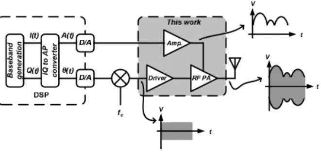
To increasing the data rate, recent wireless communication systems allow the carried information encoded in both amplitude and phase of the RF signal and therefore a linear power amplifier (PA) is required. The linearity achieved in such amplifiers by operating below their maximum output power has the drawback of low efficiency and hence reduced battery lifetime. Polar transmitter architecture, as depicted in Figure 1, can be used to overcome the trade-off between linearity and efficiency and to cope with the deficiency of CMOS technology. Therefore, the switching mode power amplifier is preferred selection for its high efficiency, where the voltage and the current waveforms are basically out of the phase, and the dc power consumption can therefore be reduced. The decomposed signal in polar coordinates, the envelope and phase signal, is recovered at the amplifier output, if the supply voltage is modulated by A(t), as clarified in Figure 1. Baseb an d ge ne ra ti on IQ t o A P co n verter
Figure 1. Block diagram of a polar modulated power amplifier.
In this paper, a fully integrated CMOS nonlinear cascode class-E amplifier is linearized based upon a polar modulation scheme. The introduced AM-AM and AM-PM distortion as supply modulation of the PA, where the AM-AM and AM-PM distortion means the amplitude and phase error on the output signal, is linearized by using a self-biased control circuit. As the control circuit modulates the stacked transistor gate voltage, the cascode transistor is degenerated into a resistance so that the distortion can be linearized. Since the class-E amplifier is performed in a switching mode operation, it is an important issue to shape the input waveform for tuning the transistor on and off. To obtain the shortest transition time from one switching state to the other, a square waveform should be applied into the class-E amplifier. This function can be realized by using the class-F amplifier as a driver stage, which can generate appropriate harmonics of the input signal and combining then into a square waveform. Moreover, for polar applications, the AM modulator is designed to modulate the supply voltage of the class-E amplifier.
For these proposed high efficiency amplifiers [1-3], implemented by CMOS technologies have used the off-chip external components to reduce the signal loss in the Si substrates. In this study, we used the CMOS 0.18 μm process technology to fabricate and 2009 Third International Symposium on Intelligent Information Technology Application
978-0-7695-3859-4/09 $26.00 © 2009 IEEE DOI 10.1109/IITA.2009.403
658
2009 Third International Symposium on Intelligent Information Technology Application
978-0-7695-3859-4/09 $26.00 © 2009 IEEE DOI 10.1109/IITA.2009.403
characterize a fully integrated, where no external components are required, 2.6 GHz polar modulated CMOS amplifier.
2. Class-E power amplifier design
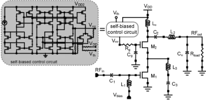
The polar modulated class-E amplifier, which consists of a class-E amplifier and a self-biased control circuit, operating at 2.6 GHz frequency band is shown in Figure 2. For reliability issues, the device-stacking topology is used. The inductor L3 and the capacitor C3
in series is used to tune out the transistor parasitic capacitance at the carrier frequency for improving the efficiency. The capacitor C2, Co and the inductor L2 are
tuned to resonance at the carrier frequency and transfer the equivalent output impedance to 50 Ω. For fully integration, the RF choke Lc is implemented by a
dc-feed with small inductance.
In a conventional class-E amplifier, the gate voltage of the transistor M2 is generally biased by a fixed point.
However, as modulating the supply voltage, the nonlinear capacitance and transconductance would be introduced and hence the AM-AM and AM-PM distortion is caused on the output signal. Furthermore, the distortion will severely degrade the system emission performance.
For compensating this distortion, we propose a self-biased control circuit, which behaves as a voltage adder. It can output a voltage of the supply VDD plus
the voltage Vth, where Vth is the threshold voltage of
the transistor. When the transistor M2 gate voltage is
modulated by the control circuit, the transistor M2 is
degenerated into a resistance and therefore the impact of the distortion can be reduced. The simulation result of the AM-AM and AM-PM distortion of the PA with and without linearization has been shown in Figure 3, in which the vertical axes represent the output signal amplitude and phase, respectively, and the horizontal axis represents the amplifier supply voltage. The result shows that when the amplifier with linearization the linear voltage relationship is achieved and the phase error is decreased from 18 degrees to 3 degrees within the supply operating range of 0.2 V to 1.8 V. As presented in [4], the phase error should be less than 5 degrees on OFDM-based signal transmission.
The characteristics of the amplifier, output power and drain efficiency, have also been simulated and shown in Figure 4. With linearization, the output power has no apparent improvement. However, the drain efficiency can be improved from 0.1 V to 1.4 V and has the maximum improvement of 15 % on the supply voltage of 0.7 V, where the improvement of drain efficiency is due to the required less power dissipation.
Figure 2. The polar modulated class-E amplifier and the detailed of self-biased control circuit.
0.0 0.5 1.0 1.5 2.0 2.5 0.0 0.2 0.4 0.6 0.8 1.0 1.2 1.4 1.6 1.8 Supply voltage (V) A m p li tude ( V ) 0 20 40 60 80 100 120 140 160 180 Ph a se ( d e g rees )
Figure 3. The comparison of the AM-AM and AM-PM distortion for the class-E amplifier.
-25 -20 -15 -10 -5 0 5 10 15 20 25 0.0 0.2 0.4 0.6 0.8 1.0 1.2 1.4 1.6 1.8 Supply voltage (V) O ut put p ow er ( d B m ) 0 5 10 15 20 25 30 35 40 D ra in ef fici enc y ( % )
Figure 4. The comparison of output power and drain efficiency of the class-E amplifier.
3. Class-F power amplifier design
A class-F amplifier uses a output filter to control the harmonic content of its drain-voltage or drain-current waveforms, thereby shaping them to reduce power dissipation by the transistor and thus to increase efficiency [5]. To accomplish this behavior, the active device has a bias point at the cutoff region for
659 659
switching operation. Also, it is known that the voltage square waveform only has the fundamental and odd harmonics.
The schematic of a class-F amplifier is shown in Figure 5. In the class-F amplifier, the output loading network consists of two parallel-tuned LC tanks, which are tuned to resonance at the fundamental and third harmonic frequency, respectively. These values of the inductors and capacitors on the tanks can be determined by F F F F C L nd C L st f harmonic f harmonic _ 3 _ 3 _ 2 _ 2 1 1 2 : 3 2 : 1 = = π π
where f is the carrier frequency.
( )s f
Figure 5. The class-F amplifier driver stage.
4. The polar modulated CMOS amplifier
and simulation result
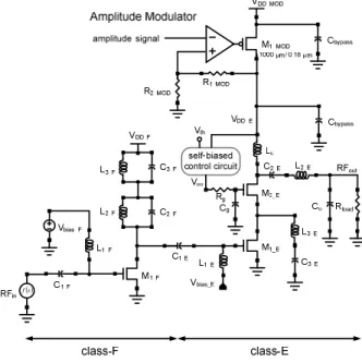
A polar modulated CMOS amplifier, which includes a polar modulated class-E output stage, a class-F driver and an amplitude modulator for modulating the class-E amplifier supply voltage, has been shown in Figure 6.
The cascode class-E amplifier with the self-biased control circuit can linearize the AM-AM and AM-PM distortion and thereby it is allowed for polar transmitter. For system-on-a-chip integration, the output matching network of the class-E amplifier is fully integrated without external passive components. Using the internal components can have the advantages of low cost and small system board area. However, the decreased efficiency can not be avoided owing to the low quality factor of the internal passive components.
The class-F is designed to output an approximately square waveform to drive the class-E amplifier with effectively switching. To perform an ideal square waveform, the effect of the transistor parasitic
capacitors has been considered on determining the component values of LC tanks. The interstage matching network was realized by using few components to achieve low loss on signal transmission.
When supply modulation, the equivalent dc load resistance of the class-E amplifier is variant. Therefore, an amplitude modulator is required to perform the constant input impedance on its input terminal and the low output load impedance. Moreover, the PMOS has large size, the width of 1000 μm, for the large dc current of the class-E amplifier.
The polar modulated CMOS amplifier has been implemented in 0.18 μm CMOS process as shown in Figure 7 and its cost area is 2x2 mm². In this work the supply voltage of the class-F driver is 1.8 V, of self-biased control circuit is 3.3 V and of the amplitude modulator is 2 V. The required driving input power of the class-F amplifier is -4 dBm.
( )s f
Figure 6. The polar modulated CMOS amplifier.
Figure 7. Layout of polar modulated CMOS amplifier.
660 660
The post-layout extraction and simulation have been done and the results are shown as follows. All of results are simulated versus the supply voltage VDD_E of
the class-E amplifier. These results are obtained by applying a DC voltage at the input voltage of the amplitude modulator. Figure 8 shows that the output signal magnitude has a linear relationship to the voltage VDD_E and the output phase error has been
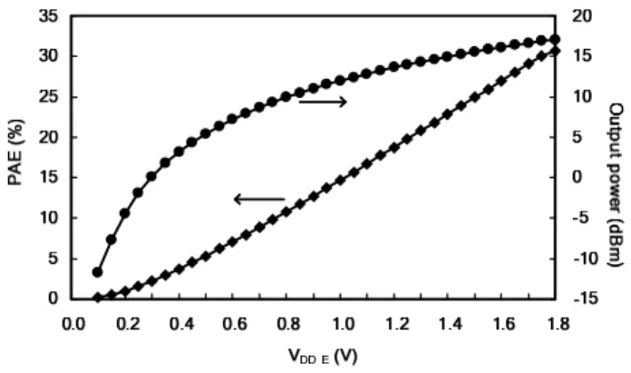
decreased down to 4 degrees within the supply operating range of 0.6 V to 1.8 V. Therefore, a CMOS class-E amplifier for polar transmitter has been demonstrated and can be achieved. Moreover, the efficiency and output power are also the important properties of the polar modulated amplifier. In Figure 9, it shows that the class-E amplifier has the maximum efficiency of 38.5 %. However, the maximum efficiency of the polar modulated amplifier is decreased to 35 %. In Figure 10, the polar modulated amplifier has the maximum output power of 17 dBm and, at the same time, it has the maximum power added efficiency (PAE) of 30%. Also, the overall power gain is 21 dB.
Figure 8. Simulation result of AM-AM and AM-PM.
Figure 9. The comparison of drain efficiency.
Figure 10. PAE and output power.
5. Conclusions
An integration of the polar modulated class-E amplifier with a class-F driver in 0.18 μm CMOS process has been presented. The AM-AM and AM-PM distortion of the class-E output stage is compensated by using the proposed self-biased control circuit. The linear relationship of the output signal magnitude versus the class-E supply voltage is obtained and the AM-PM is reduced down to only 4 degrees. The maximum output power is 17 dBm while having the maximum PAE of 30 %. And it has the maximum power gain of 21 dB.
References
[1] K. L .R. Mertens and M. S. J. Steyaert, “A 700-MHz 1-W Fully Differential CMOS Class-E Power Amplifier”, IEEE
Journal of Solid-State Circuit, Vol. 37, 2002, pp. 137-141.
[2] C. Yoo and Q. Huang, “A Common-Gate Switched 0.9-W Class-E Power Amplifier with 41% PAE in 0.25-μm CMOS”, IEEE Journal of Solid-State Circuit, Vol. 36, 2001, pp. 823-830.
[3] K. C. Tsai and P. R. Gray, “A 1.9-GHz 1-W CMOS Class-E Power Amplifier for Wireless Communications”,
IEEE Journal of Solid-State Circuit, Vol. 34, July 1999, pp.
962-970.
[4] M. Tolonen and S. Lindfors, “System Requirements for OFDM Polar Transmitter”, Proceedings of the 2005
European Conference on Circuit Theory and Design, Vol. 3,
August 2005, pp. 69-72.
[5] F .H. Raab, “An Introduction to Class-F Power Amplifiers”, RF Design, Vol. 19, No. 5, May 1996, pp. 79-84.
661 661