Nitrogen Effects on the Integrity of Silicon Dioxide Grown on
Polycrystalline Silicon
Chao Sung Lai,aChyuan Haur Kao,a,zChung Len Lee,band Tan Fu Leib a
Department of Electronics Engineering, Chang Gung University, Tao Yuan, Taiwan b
Department of Electronics Engineering, National Chiao Tung University, Hsinchu, Taiwan
In this paper, we describe a simple technique to achieve a thin nitrided polyoxide film, only requiring an extra nitrogen implan-tation to be compatible with the floating gate nonvolatile memory process. The integrity of polyoxides is improved by using the through-silicon-gate nitrogen implantation. Nitridation can be achieved by implanting nitrogen into polysilicon gate followed by a high temperature annealing to drive the nitrogen atoms across the polysilicon, through the polyoxide, and to incorporate nitrogen at the polyoxide/polysilicon interface. The nitrogen-rich layer formed during the driven-in process not only strengthens the polyoxide structure but also improves the polyoxide quality. Improvements of electrical characteristics such as a low leakage current, a low electron trapping, and a high breakdown field for both positive and negative biases have been observed. © 2007 The Electrochemical Society. 关DOI: 10.1149/1.2767854兴 All rights reserved.
Manuscript submitted March 1, 2007; revised manuscript received June 11, 2007. Available electronically August 15, 2007.
In order to obtain good data retention characteristics for nonvola-tile memory devices, the interpolysilicon oxides共polyoxides兲 with low conductivity, high breakdown fields and high charge to break-down are required.1-7The polyoxides grown on polysilicon have a higher leakage current and a lower dielectric strength than those of oxides with comparable thickness grown on single crystal silicon, especially when a positive bias is applied to the top electrode. This is attributed to the rough asperities at the polyoxide/polysilicon in-terface and nonuniformities in polyoxide film thickness, and en-hanced localized electric field due to the enen-hanced oxidation rate at polysilicon grain boundaries. Also, the integrity of polyoxide mainly depends on growth oxidants or postoxidation annealing.8,9
Previous studies showed that the polyoxides grown in N2O am-bient have good oxide integrity and excellent electrical characteris-tics. This improvement is largely owing to the incorporation of ni-trogen in N2O ambient.10-13It is also well known that the oxynitride films grown in NO or N2O ambient with nitrogen incorporation as gate dielectrics of metal-oxide-semiconductor field effect transistors have been reported to exhibit good electrical and reliability characteristics.14-17This is due to the nitrogen incorporation at gate oxide/silicon interface, which can avoid hot-carrier damages, pre-vent boron penetration and improve interface endurance to Fowler-Nordheim共FN兲 stress.18-23But normal nitridation with NO or N2O ambient introduces a small amount of nitrogen at Si/SiO2interface, which is insufficient to prevent boron penetration when the oxide is thinner than 3.0 nm. Increasing the temperature or time to increase the nitrogen concentration in oxides will result in a thicker oxide and redistribution of channel doping profile.24,25So, the direct im-plantation of nitrogen into the silicon substrates has been proposed as a nitridation technique for ultrathin gate oxides.26-30Some studies have also been reported that gate oxides grown on nitrogen im-planted silicon substrates exhibit superior electrical properties, ef-fectively prevent boron penetration and improve the hot-carrier resistance.31-36
To achieve a thin nitrided polyoxide film, a simple technique has been described in this study. An extra nitrogen implantation process has been used for the floating gate nonvolatile memory device ap-plications. The integrity of polyoxide films has been improved by nitrogen implantation process. Due to the nitrogen incorporation into polyoxide films, the improved electrical properties such as low leakage current, low electron trapping, and high breakdown field have been observed for both positive and negative bias conditions.
Experimental
In this study, n+-polysilicon/polyoxide/n+-polysilicon capacitor structures were fabricated by following process sequence. p-Type Si
wafers were thermally oxidized with a thickness of 100 nm. Then, the polysilicon film共poly-1兲 with a thickness of 300 nm was depos-ited by low-pressure chemical vapor deposition at a substrate tem-perature of 625°C. The poly-1 as a bottom electrode was doped by POCl3diffusion process. To activate the dopant, a 1 h drive-in pro-cess was performed in N2ambient at a temperature of 900°C. The sheet resistance of polysilicon film was⬃22 ⍀/䊐.
Polyoxides with a thickness of about 13 nm were grown in a pure O2 ambient at 850°C. Then, the second layer of polysilicon 共poly-2兲 with a thickness of 300 nm for the top electrode was de-posited and also doped with POCl3. The sheet resistance of poly-2 was ⬃22 ⍀/䊐. After 15 nm pad oxide was grown in a pure O2 ambient at 850°C, samples were implanted at 25 keV with nitrogen of various doses from 1⫻ 1013, 1⫻ 1014, 1⫻ 1015to 5 ⫻ 1015ions/cm2, and followed by N
2ambient annealing for 1 h at 850°C. Then, the poly-2 was defined and on all samples a 100 nm thick oxide was grown via wet oxidation as a passivation layer. Contact holes were opened, and Al was deposited and patterned to form capacitors. Finally, all devices were sintered at 350°C for 40 min in N2ambient, which can improve metallurgy between poly-silicon and metal film, and it can be further reduced contact resis-tance.
The thickness of polyoxide film was determined by high-frequency共100 kHz or 1 MHz兲 capacitance-voltage 共C-V兲 measure-ment. The current-voltage characteristics of all samples were mea-sured using HP4156 semiconductor parameter analyzer.
Results and Discussion
The secondary ion mass spectrometry共SIMS兲 depth profiles of nitrogen for those devices implanted with 0, 1⫻ 1013, 1⫻ 1014, 1⫻ 1015, and 5⫻ 1015ions/cm2followed by annealing at 850°C for 1 h in N2ambient are shown in Fig. 1. For the highest implanted nitrogen sample共5 ⫻ 1015ions/cm2兲 in the figure, it can be seen that a highest nitrogen peak is located inside the top polysilicon 共poly-2兲 layer near the as-implanted peak, and nitrogen concentra-tion is gradually lowered down along the polysilicon layer and piled up in the polyoxide/polysilicon interfaces. When the implanted ni-trogen dose is reduced, the nini-trogen peak located inside the poly-2 film is also lowered, even down to base level as the nonimplanted sample. But it can be found that most of the nitrogen doses of the lighter implanted samples such as 1⫻ 1013, 1⫻ 1014共ions/cm2兲 have been diffused toward the polyoxide/polysilicon interfaces and piled up at the interfaces to incorporate into the polyoxide. For higher nitrogen dose samples, the nitrogen can be incorporated more at the polyoxide/polysilicon interfaces. This is due to the postim-plantation high temperature annealing process 共850°C for 1 h兲 to drive and diffuse the implanted nitrogen deeper toward the polysili-con layer and accumulated nitrogen to pile up in the polyoxide/ polysilicon interfaces.
z
E-mail: [email protected]
Journal of The Electrochemical Society, 154共10兲 H883-H886 共2007兲
0013-4651/2007/154共10兲/H883/4/$20.00 © The Electrochemical Society H883
) unless CC License in place (see abstract).
ecsdl.org/site/terms_use
address. Redistribution subject to ECS terms of use (see
140.113.38.11
Final thicknesses of all samples determined by C-V measure-ments are shown in Fig. 2. The thickness of nonimplanted sample is about 13.2 nm and the thickness of polyoxide film is gradually de-creased with increasing the nitrogen implantation doses. The thick-ness of highest nitrogen-implanted共5 ⫻ 1015ions/cm2兲 sample is 15% thinner than that of the nonimplanted sample. It may be due to the nitrogen-rich layer formation. The dielectric constant is in-creased when nitrogen piled up in the polyoxide/polysilicon inter-faces.
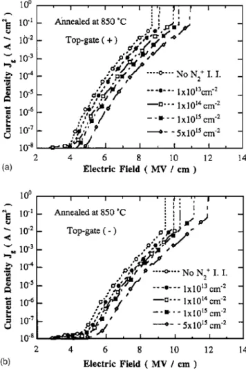
Figure 3a and b shows the J-E characteristics of polyoxide films implanted with various doses of nitrogen for positive gate bias 共elec-tron injection from the bottom poly-1 electrode兲 and negative gate bias共electron injection from the top poly-2 electrode兲, respectively. It can be seen that the nitrogen-implanted polyoxide films exhibit lower leakage currents and higher breakdown electric fields than that of the nonimplanted sample for both positive and negative bi-ases. The improvements of J-E characteristics are believed due to the nitrogen implantation in polyoxide films. The nitrogen can pas-sivate the dangling bonds and break the strained Si–O bonds to form more strong Si–N bonds in the polysilicon/polyoxide interfaces. So,
the local stress can be relaxed in the oxide network and made the polysilicon/polyoxide interface morphology smoother. It is indicated that the stress between polyoxide and polysilicon films affects the polyoxide breakdown strength, decreasing the oxide stress increases the breakdown strength.37 In this experiment, the leakage current and breakdown field for both positive and negative biases are im-proved with increasing the dose of nitrogen.
It has been reported that the effective barrier height and leakage current of polyoxide were mainly determined by polyoxide/ polysilicon interface roughness.5The above J-E data in the form of FN plot共J/E2vs 1/E兲 is shown in Fig. 4a and b for the top gate with positive and negative biases, respectively. The effective barrier height extracted from FN plot was shown in Fig. 5. For the positive top-gate bias, the calculated effective barrier heights can be in-creased from 1.51 eV共for the nonimplanted polyoxide兲 to 1.76 eV 共for the highest nitrogen-implanted polyoxide兲. For both positive and negative top-gate biases, the effective barrier heights can be gradually increased with increasing the nitrogen implantation doses. The effective barrier height is related to polyoxide/polysilicon inter-face texture, increasing the barrier height reduces the roughness of the polyoxide/polysilicon interface. This implies that the nitrogen implantation in polyoxide samples can form a nitrogen-rich layer in the polyoxide/polysilicon interfaces after high temperature anneal-ing treatment. It can further improve the polyoxide interface rough-ness and increase the barrier height. The barrier heights of all samples with negative top-gate bias共electron injection from the top
Figure 1. The SIMS depth profiles of nitrogen for the devices implanted
with 1⫻ 1013, 1⫻ 1014, 1⫻ 1015and 5⫻ 1015ions/cm2and without
ni-trogen implantation followed by annealing at 850°C in N2ambient.
Figure 2. The polyoxide thicknesses of the devices implanted with various
doses of nitrogen.
Figure 3. The J-E characteristics of polyoxides implanted with various
doses of nitrogen for共a兲 positive gate bias 共electron injection from the bot-tom poly-1 gate兲, and 共b兲 negative gate bias 共electron injection from the top poly-2 gate兲.
H884 Journal of The Electrochemical Society, 154共10兲 H883-H886 共2007兲
H884
) unless CC License in place (see abstract).
ecsdl.org/site/terms_use
address. Redistribution subject to ECS terms of use (see
140.113.38.11
poly-2 electrode兲 are larger as compared with positive top-gate bias 共electron injection from the bottom poly-1 electrode兲. This also
im-plies that the top poly-2/polyoxide interface may be smoother than that of bottom poly-1/polyoxide interface in spite of the sample with or without nitrogen implantation.
The histogram of breakdown electric field for all samples is shown in Fig. 6a and b for positive and negative biases, respectively. It can be seen that the breakdown electric field is increased with increasing nitrogen doses. All samples with positive top-gate bias exhibit a higher conductance and lower dielectric breakdown fields than those of negative top-gate bias. This is due to the enhanced oxidation at the bottom polysilicon grain boundaries, which induces a rougher bottom poly-1/polyoxide interface as compared to the top poly-2/polyoxide interface.8,9
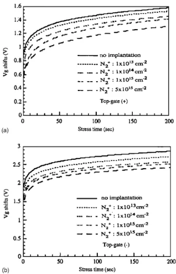
The charge trapping characteristics of all nitrogen implanted samples have been investigated. Figure 7a and b shows the gate voltage shift vs time under a constant current stressing of 100A/cm2for both top-gate positive and negative biases, respec-tively. The gate voltage increases due to the electron trapping. It is observed that the nitrogen implanted samples show lower electron trapping rates than that of the nonimplanted sample. The electron trapping rates are decreased with increasing the nitrogen implanta-tion for both positive and negative biases. Due to the local high stress in polyoxide films, there are many strained bonds within polyoxides.2These strained bonds can easily broken by high energy electrons, resulting in a dielectric breakdown when a field is applied to the polyoxide films. When nitrogen was implanted into the
poly-Figure 4. Fowler-Nordheim plots共J/E2vs 1/E兲 for the polyoxides implanted
with various doses of nitrogen for共a兲 positive gate bias and 共b兲 negative gate bias.
Figure 5. The effective barrier heights have been extracted from
Fower-Nordheim plot for the polyoxides implanted with various doses of nitrogen under both positive and negative top-gate biases.
Figure 6. The histogram of breakdown electric field for the polyoxide
im-planted with various doses of nitrogen for共a兲 positive gate bias and 共b兲 negative gate bias.
H885
Journal of The Electrochemical Society, 154共10兲 H883-H886 共2007兲 H885
) unless CC License in place (see abstract).
ecsdl.org/site/terms_use
address. Redistribution subject to ECS terms of use (see
140.113.38.11
silicon layer, the nitrogen-rich layer could be formed after the high temperature annealing process. The nitrogen-rich layer not only strengthens polyoxide structure but also improves the polyoxide quality.
Conclusion
In conclusion, it is found that polyoxide with incorporated nitro-gen had a lower leakage current and a higher breakdown field for both positive and negative biases. The implanted nitrogen followed by a high temperature annealing drive the nitrogen across the poly-silicon, through the polyoxide, and incorporate nitrogen at the polyoxide/polysilicon interface. These improvements have been ob-served due to the nitrogen incorporation in the polyoxide films. The nitrogen can passivate the dangling bonds and break the strained Si–O bonds to form strong Si–N bonds in the polysilicon/polyoxide interfaces. Both the strength and quality of polyoxide films can be improved, due to the nitrogen-rich layer formation after high tem-perature annealing process.
Chang Gung University assisted in meeting the publication costs of this article.
References
1. T. C. Hamada, Y. Saito, M. Hirayama, H. Aharoni, and T. Ohmi, IEEE Electron
Device Lett., 22, 423共2001兲.
2. L. Faraone, R. D. Vibronek, and J. T. Mcginn, IEEE Trans. Electron Devices,
ED-32, 577共1985兲.
3. L. Faraone and G. Harbeke, J. Electrochem. Soc., 133, 1410共1986兲.
4. C. Cobianu, O. Popa, and D. Dascalu, IEEE Electron Device Lett., 14, 213共1993兲. 5. J. C. Lee and C. Hu, IEEE Trans. Electron Devices, ED-35, 1063共1988兲. 6. P. Candelier, F. Mondon, B. Guillaumont, G. Reimbold, and F. Martin, IEEE
Elec-tron Device Lett., 18, 306共1997兲.
7. T. One, T. Mori, T. Ajioka, and T. Takayashiki, Tech. Dig. - Int. Electron Devices
Meet., 1985, 380.
8. L. Faraone, IEEE Trans. Electron Devices, ED-33, 1785共1986兲.
9. S. L. Wu, T. Y. Lin, C. L. Lee, and T. F. Lei, IEEE Electron Device Lett., 14, 113 共1994兲.
10. C. S. Lai, T. F. Lei, and C. L. Lee, IEEE Trans. Electron Devices, 43, 1共1996兲. 11. C. H. Kao, C. S. Lai, and C. L. Lee, IEEE Trans. Electron Devices, 45, 1927
共1998兲.
12. C. H. Kao, C. S. Lai, and C. L. Lee, IEEE Electron Device Lett., 18, 526共1997兲. 13. C. H. Kao, C. S. Lai, and C. L. Lee, J. Electrochem. Soc., 153, 128共2006兲. 14. T. Sasaki, K. Kuwazawa, K. Tanaka, J. Kato, and Dim-Lee Kwong, IEEE Electron
Device Lett., 24, 150共2003兲.
15. H. Hwang, W. Ting, D.-L. Kwong, and J. Lee, IEEE Electron Device Lett., 12, 495 共1991兲.
16. W.-C. Yang, C.-F. Chen, and K.-M. Chang, Electron Devices Solid-State Circuits,
2003 IEEE Conference, p. 349共2003兲.
17. Y. Okayama, K. Kasai, T. Yamaguchi, A. Ooishi, M. Takayanagi-Takagi, F. Mat-suoka, and M. Kinugawa, VLSI Technology, Digest of Technical Papers
Sympo-sium, p. 220共1998兲.
18. B. S. Doyle and A. Philipossian, IEEE Electron Device Lett., 18, 267共1997兲. 19. V. P. Gopinath, V. Hornback, Y. Le, A. Kamath, L. Duong, J. Lin, M. R.
Mirabe-dini, and W. C. Yeh, Gate Insulator, 2003.IWGI, Extended Abstracts of
Interna-tional Workshop, November, p. 50共2003兲.
20. Y. Y. Chen, M. Gardner, J. Fulford, D. Wristers, A. B. Joshi, L. Chung, and D. L. Kwong, VLSI Technology, Systems, and Applications, International Symposium, p. 86共1999兲.
21. Y. Okada, P. J. Tobin, K. G. Reid, R. I. Hegde, B. Maiti, and S. A. Ajuria, IEEE
Trans. Electron Devices, 41, 608共1994兲.
22. M. Bhat, D. J. Wristers, L.-Kai Han, J. Yan, H. J. Fulford, and D.-L. Kwong, IEEE
Trans. Electron Devices, 42, 907共1995兲.
23. M.-S. Joo, I.-S. Yeo, C.-H. Lee, H.-J. Cho, S.-A. Jang, and S.-K. Lee, IEEE
Elec-tron Device Lett., 20, 445共1999兲.
24. M. Bhat, D. J. Wristers, L.-K. Han, J. Yan, H. J. Fulford, and D.-L. Kwong,
International Electron Devices Meeting, p. 329共1994兲.
25. M. K. Mazumder, A. Teramoto, J. Komori, and Y. Mashiko, ICMTS Proceedings of
Microelectronic Test Structures, p. 103共2001兲.
26. S. Hadda and M. S. Liang, IEEE Electron Device Lett., 8, 58共1987兲. 27. A. J. Bauer, P. Mayer, L. Frey, V. Haublein, and H. Ryssel, Ion Implantation
Technology Proceedings, 1, p. 26共1998兲.
28. L. K. Han, S. Crowder, M. Hargrove, E. Wu, S. H. Lo, F. Guarin, E. Crabbe, and L. Su, Tech. Dig. - Int. Electron Devices Meet., 1997, 643.
29. B. Yu, D.-H. Ju, W.-C. Lee, N. Kepler, T.-J. King, and C. Hu, IEEE Trans. Electron
Devices, 45, 1253共1998兲.
30. A. I. Chou, C. Lin, K. Kumar, P. Chowdhury, M. Gardner, M. Gilmer, J. Fulford, and J. C. Lee, IEEE International Reliability Physics Symposium, 35th Annual
Proceedings, p. 174共1997兲.
31. I.-H. Nam, J. S. Sim, S. I. Hong, B.-G. Park, J. D. Lee, S.-W. Lee, M.-S. Kang, Y.-W. Kim, K.-P. Suh, and W. S. Lee, IEEE Trans. Electron Devices, 48, 2310 共2001兲.
32. C. T. Liu, Y. Ma, H. Luftman, and S. J. Hillenius, IEEE Electron Device Lett., 18, 212共1997兲.
33. C. T. Liu, Y. Ma, J. Becerro, S. Nakahara, D. J. Eaglesham, and S. J. Hillenius,
IEEE Electron Device Lett., 18, 105共1997兲.
34. Y. Y. Chen, D. L. Kwong, M. Gardner, and J. Fulford, Solid-State Device Research
Conference, p. 292共1998兲.
35. C.-C. Chen, H.-C. Lin, C.-Y. Chang, C.-C. Huang, C.-H. Chien, T.-Y. Huang, and M.-S. Liang, Plasma Process-Induced Damage, 5th International Symposium, p. 121共2000兲.
36. A. J. Bauer, P. Mayer, L. Frey, V. Haublein, and H. Ryssel, Ion Implantation
Technology Proceedings, 1998 International Conference, Vol. 1, p. 30共1998兲.
37. H. N. Chern, C. L. Lee, and T. F. Lei, IEEE Electron Device Lett., 15, 181共1994兲.
Figure 7. The gate voltage shifts共⌬Vg兲 vs time of the polyoxides implanted with various doses of nitrogen under共a兲 +Vgand共b兲 −Vgconstant current 共100 A/cm2兲 stressing, respectively.
H886 Journal of The Electrochemical Society, 154共10兲 H883-H886 共2007兲
H886
) unless CC License in place (see abstract).
ecsdl.org/site/terms_use
address. Redistribution subject to ECS terms of use (see
140.113.38.11