This content has been downloaded from IOPscience. Please scroll down to see the full text.
Download details:
IP Address: 140.113.38.11
This content was downloaded on 28/04/2014 at 18:27
Please note that terms and conditions apply.
Nonvolatile floating gate memory containing AgInSbTe–SiO2 nanocomposite layer and
capping the HfO2/SiO2 composite blocking oxide layer
View the table of contents for this issue, or go to the journal homepage for more 2012 Nanotechnology 23 225703
(http://iopscience.iop.org/0957-4484/23/22/225703)
Nanotechnology 23 (2012) 225703 (8pp) doi:10.1088/0957-4484/23/22/225703
Nonvolatile floating gate memory
containing AgInSbTe–SiO
2
nanocomposite layer and capping the
HfO
2
/SiO
2
composite blocking oxide layer
Kuo-Chang Chiang and Tsung-Eong Hsieh
Department of Materials Science and Engineering, National Chiao Tung University, 1001 Ta-Hsueh Road, Hsinchu 30010, Taiwan, Republic of China
E-mail:[email protected]
Received 12 January 2012, in final form 3 April 2012 Published 10 May 2012
Online atstacks.iop.org/Nano/23/225703 Abstract
An extremely large memory window shift of about 30.7 V and high charge storage density = 2.3 × 1013cm−2at ±23 V gate voltage sweep were achieved in the nonvolatile floating gate memory (NFGM) device containing the AgInSbTe (AIST)–SiO2nanocomposite
as the charge trap layer and HfO2/SiO2as the blocking oxide layer. Due to the deep trap sites
formed by high-density AIST nanocrystals (NCs) in the nanocomposite matrix and the high-barrier-height feature of the composite blocking oxide layer, a good retention property of the device with a charge loss of about 16.1% at ±15 V gate voltage stress for 104s at the test temperature of 85◦C was observed. In addition to inhibiting the Hf diffusion into the programming layer, incorporation of the SiO2layer prepared by plasma-enhanced chemical
vapor deposition in the sample provided a good Coulomb blockade effect and allowed significant charge storage in AIST NCs. Analytical results demonstrated the feasibility of an AIST-SiO2nanocomposite layer in memory device fabrication with a simplified processing
method and post-annealing at a comparatively low temperature of 400◦C in comparison with
previous NC-based NFGM studies.
(Some figures may appear in colour only in the online journal)
1. Introduction
Nonvolatile floating gate memory (NFGM) is the key component of portable electronic products in the present day. With the progress of device scale-down and demand of high storage capacity, relevant studies have been performed in order to overcome the difficulties encountered in conventional memory devices containing poly-silicon (poly-Si) as the programming layer [1–3]. Recently, NFGM devices utilizing either semiconductor or metallic nanocrystals (NCs) as the discrete charge storage traps have attracted considerable attention due to their advantages of low lateral leakage current, low power consumption, high operative efficiency and better endurance [4–6]. Tiwari et al first implanted
the Si NCs in NFGM [7] and, afterwards, various NFGMs containing semiconductor NCs such as germanium (Ge) [8] and SiGe [9] or transition metal NCs such as silver (Ag) [1], ruthenium (Ru) [10], tungsten (W) [11], cobalt (Co) [12], platinum (Pt) [13], gold (Au) [14], nickel (Ni) [15], molybdenum (Mo) [16], chromium (Cr) [17] and iridium (Ir) [18] were reported. Among these, the transition metal NCs provided better memory performance and retention characteristics due to their high thermal stability and suitable physical properties [10–18]. The maximum memory window (1VFB) shift = 15 V at ±17 V gate voltage sweep was
achieved in NFGM by containing Cr NCs as the charge storage traps [17]. However, complicated processing methods such as pulsed-laser deposition (PLD) [3], atomic layer
Nanotechnology 23 (2012) 225703 K-C Chiang and T-E Hsieh
deposition (ALD) [10] and ion implantation [15] are usually required to deposit the thin metal layers for subsequent NC formation. Another difficulty encountered in NC-based NFGMs is that post-annealing at relatively high temperatures (above 600◦C) is usually required to accomplish high-density NCs with uniform dispersion. Inadequate thermal processing might cause either oxidization of NCs or the interdiffusion in between NCs and the surrounding oxide, leading to the degradation of charge-capture efficiency of NCs [19]. Moreover, the charge trapping layers have to be capped by appropriate dielectric layers in order to reduce the leakage current and alleviate the charge injection in between the gate and programming layer for reliable data retention in NC-based NFGM [20]. HfO2 is the most promising
material for such purposes due to its relatively high dielectric constant (k = 25) and large bandgap (Eg =
5.68 eV) properties [21]. Nevertheless, the relatively low recrystallization temperature (about 500◦C) and high oxygen diffusivity of HfO2 might lead to high leakage current
and poor device performance [21–23]. Nitrogen (N2) [22]
or alumina (Al2O3) [23] have been incorporated in HfO2
to eliminate those deficiencies; however, it might interrupt the stoichiometry of the deposited layer and escalate the complication of fabrication processes.
Chalcogenides are well-known recording media for optical data storage due to their ultrafast phase-transition rates and comparatively low recrystallization temperatures [24]. When the chalcogenides are implanted in NCs, these unique characteristics enable a low-temperature post-annealing with short time duration that may suppress the undesired oxidation and interdiffusion mentioned previously. Moreover, chalcogenides possess the Egand electron affinities similar to
those of Si and their charge trapping effects are suitable for NFGM applications [25]. The feasibility of chalcogenides to NFGM has been demonstrated by the study which reports the 1VFBshift = 6.6 V at ±8 V gate voltage sweep and charge
storage density = 5.2 × 1012 cm−2in the device containing a sole AgInSbTe (AIST)–SiO2nanocomposite programming
layer [26]. In this study, the AIST-SiO2nanocomposite-based
NFGM capped by the HfO2/SiO2 composite blocking
oxide layer is prepared and the correlations of electrical performance to microstructures of such a memory device are evaluated accordingly. In particular, the effects of barrier-height configuration on the charge trapping and transport behaviors of samples are discussed in terms of the analytical results presented as follows.
2. Experiments
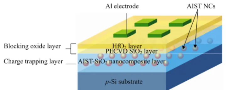
Figure1schematically illustrates the NFGM device structure prepared in this study. Such a metal–insulator–semiconductor (MIS) structure was fabricated on p-type Si(100) substrates (resistivity = 1–20 cm) pre-cleaned by a standard RCA process and immersed in a diluted HF solution to remove native oxides. First, the AIST (doped Sb2Te
alloy with a stoichiometry of Ag0.1In0.2Sb2Te supplied by
Solar Applied Materials Technology Co., Taiwan, ROC) powder was pressed into disc pellets 12 mm in diameter.
Figure 1. Schematic illustration of NFGM device structure.
After mounting an appropriate number of AIST pellets on a 3 inch quartz sputtering target, the deposition of the AIST-SiO2nanocomposite layer was carried out in a vacuum
system with background pressure better than 2 × 10⁻⁶Torr. About a 30 nm thick AIST-SiO2 nanocomposite layer was
deposited on the Si substrate via the target-attachment sputtering method [26,27] under the conditions of working pressure = 3 mTorr, rf gun power = 100 W and argon (Ar)/N2 inlet gas flow ratio = 10:2 (in units of sccm).
The purpose of N2 incorporation during sputtering is to
suppress the oxygen defects in the nanocomposite layer [28] and enhance the surface polarization effect [29] so as to improve the leakage current property. Subsequently, the HfO2/SiO2 /AIST-SiO2 NFGM sample was prepared by
depositing a 7 nm thick PECVD SiO2 layer on the
AIST-SiO2 nanocomposite layer using tetraethoxysilane (TEOS)
as the precursor at a temperature of 250◦C followed by the sputtering deposition of a 7 nm thick HfO2 layer at
working pressure = 3 mTorr, rf gun power = 100 W and Ar inlet gas flow = 10 sccm. Afterwards, the sample was annealed by using an infrared convey furnace at 400◦C for 90 s in atmospheric ambient in order to induce the recrystallization of the AIST phase in the nanocomposite layer. Finally, a 300 nm thick aluminum (Al) electrode 0.2 mm in diameter was deposited by e-beam evaporation to complete the sample preparation. Notably, the post-annealing condition delineated above has been optimized for achieving the best device performance. It was found that inadequate annealing would cause either insufficient recrystallization or excessive oxidation of the AIST phase, leading to undesired NFGM properties.
Transmission electron microscopy (TEM, FEI TECNAI G2 F20 S-TWIN) equipped with an energy dispersive spectroscopy (EDX, Link ISIS 300) was adopted to characterize the microstructures of the NFGM samples. Evolutions of composition and chemical status of elements in nanocomposite layers were analyzed by an x-ray photoelectron spectroscopy (XPS, PHI Quantera SXM). Capacitance–voltage (C–V) and charge retention properties of NFGM devices were evaluated by an HP 4284A precision LCR meter at a frequency of 1 MHz. The current–voltage (I–V) profiles were measured by an HP 4156B semiconductor parameter analyzer in conjunction with a probe tester (SANWA, WM-365A-1) in order to explore the conduction mechanisms of the sample.
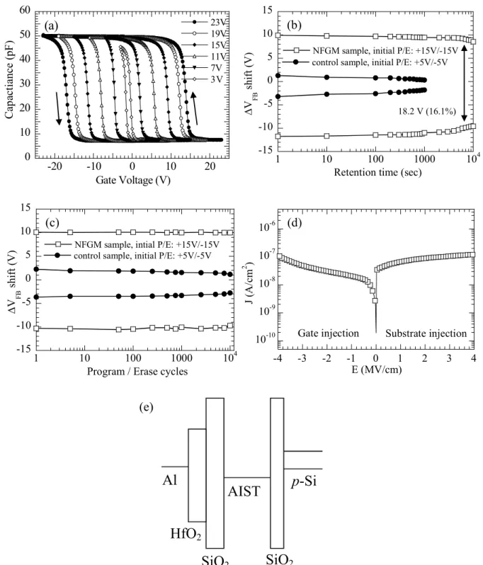
Figure 2. (a) C–V profiles for the NFGM device subjected to gate voltage sweep ranging from ±3 to ±23 V. (b) Charge retention characteristics at 85◦
C and (c) endurance characteristics of NFGM and controlled samples subjected to ±15 V and ±5 V gate voltage stress, respectively. (d) J–E profiles and (e) schematic illustration of band diagram for NFGM sample.
3. Results and discussions
Figure 2(a) shows the C–V profiles of the NFGM sample subjected to the gate voltage sweep ranging from ±3 to ±23 V. A counterclockwise hysteresis with extremely large 1VFBshift = 30.7 V at ±23 V voltage sweep can be readily
seen, implying the saturated substrate injection of charges into the AIST NCs which serve as the charge storage traps.
The counterclockwise hysteresis is known to correlate with the electron transport mechanism [5]. Namely, by applying the positive bias on the gate to form the program state, the electrons injected from the Si substrate would be trapped in the AIST NCs. An increase of bias is required for further incoming electrons to overcome the repulsive electric field built by the trapped electrons, consequently resulting in the positive 1VFB shift. On the other hand, when a negative
Nanotechnology 23 (2012) 225703 K-C Chiang and T-E Hsieh
bias is applied on the gate to form the erase state, the electrons would escape from the AIST NCs to the Si substrate. Sufficiently high bias would be required to remove the charges trapped in AIST NCs and hence induce the negative 1VFBshift. The maximum charge storage density was found
to be 2.3 × 1013 cm−2 according to the formula [23], N = (Cacc1VFB)/(qA), where Cacc is the accumulation
capacitance, q is the electron charge and A is the electrode area. In comparison with the C–V properties of NFGM containing a sole AIST-SiO2 nanocomposite layer [26], the
capping of the HfO2/SiO2 composite blocking oxide layer
indeed improved the electrical performance of the NFGM device.
The highly symmetrical 1VFB shifts reveal an
equi-librium of saturated electron trapping and hole trapping in the AIST NCs with excellent charge retention during the forward and reverse bias sweeps in the NFGM sample. In particular, the enlargement of 1VFB shift in the positive
bias side indicates an increase of electron storage in AIST NCs under positive bias [13]. Our experiment also observed that the electrical properties of the NFGM sample barely changes with storage time whereas that of the sole-layer AIST-SiO2 NFGM device degrades moderately with the
increase of sample storage time. It is believed that the PECVD SiO2layer may effectively passivate the device and
terminate the environmental attacks. The enhancement of charge-capture efficiency in the sample will be discussed in terms of the microstructure and composition analyses presented as follows.
In order to illustrate the operational reliability of the NFGM sample, the charge retention and endurance charac-teristics were investigated and compared with the measured results of the sample without the HfO2/SiO2 composite
blocking oxide layer (i.e. the controlled device containing a sole AIST-SiO2 nanocomposite layer). Figure 2(b) presents
the charge retention characteristics of the NFGM samples in which the 1VFB shifts subjected to alternating electron
(program) and hole (erase) injections were measured up to 104 s under the gate voltage stress for 10 s. We note that severe deterioration of the 1VFB shift is observed in the
controlled sample when gate voltage stress exceeds ±8 V. As a result, the gate voltage stress conditions varied for various samples, i.e. the NFGMs with the HfO2/SiO2capping layer
were measured at ±15 V voltage stress whereas the controlled sample without the HfO2/SiO2 capping layer was measured
at ±5 V voltage stress. At the test temperature of 85◦C, a large 1VFB shift of about 18.2 V and the charge loss of
about 16.1% were observed in the NFGM sample capped by the HfO2/SiO2 oxide layer. As to the controlled sample, it
exhibited poor device durability since the retention property diminished after 103s. The large amount of charges sustained for data storage is attributed to the deep trap sites in the AIST-SiO2 nanocomposite layer, which suppress the direct
tunneling from the trapping layer into the substrate [30]. In addition, it is known that the increase of the 1VFB shift is
correlated to the reduction of charge injection from the gate through the blocking oxides [31] and a high-quality blocking oxide layer with appropriate thickness is essential to the satisfied charge storage capability of the NFGM [17].
Figure 2(c) depicts the endurance characteristics of NFGM samples, with and without the HfO2/SiO2 capping
layer, measured at the pulse gate voltage stress of ±15 V and ±5 V for 10 ms duration, respectively. For the sample containing HfO2/SiO2capping layer, the 1VFBshift
remained stable without significant decay after 104 pulse cycle operations. This is ascribed to the high-barrier feature of the HfO2/SiO2 oxide layer which effectively inhibits the
injection of charge trapped in AIST NCs to the gate electrode so as to yield a stable 1VFB shift property during the
cycle operation. In comparison with previous studies utilizing at least 20 nm thick blocking oxide layers [12–19], the HfO2/SiO2 composite oxide layer with thickness less than
15 nm is able to suppress the charge injection in the NFGM and implies the good retention property. This is ascribed to the insertion of a PECVD SiO2layer with relatively large Eg
(=9 eV) which renders a sufficiently high barrier to alleviate the charge tunneling.
Figure 2(d) presents the profiles of leakage current density versus applied bias field (J–E) of NFGM samples deduced by the I–V measurement. A relatively low leakage current and highly symmetrical J–E profile can be readily seen. The symmetry in the J–E profiles resulted from the similarity in material properties and conduction mechanisms across the Al gate/nanocomposite and nanocomposite/Si substrate interfaces [32–34]. This is illustrated by the plot of band diagrams for the sample in the cases of gate and substrate injections depicted in figure2(e). We note that the presence of material species in figure2(e) is plotted in accord with the results of TEM and XPS analyses. As shown in this plot, the charge trapping layer is, in fact, enclosed in between two SiO2layers and thus a symmetrical J–E profile
could be achieved. Moreover, the high-barrier-height PECVD SiO2 layer in the composite blocking oxide layer is able to
suppress the charge injection from the gate to AIST NCs. It consequently enhances the Coulomb blockade effect and drastically reduces the leakage current density of the sample to a value as low as 150 nA cm−2in the gate injection case. As revealed by subsequent XPS analysis, the low leakage current property is also ascribed to the strong surface polarization effect [29] at the AIST/SiO2interface induced by the N2gas
incorporation during sputtering.
Bersuker et al reported the escalation of oxygen vacancy concentration in the underlying SiO2 matrix due to the
interdiffusion of HfO2 [35]. When the oxygen deficiency
occurs in the vicinity of the Si substrate, the reduction of effective barrier height of the SiO2 layer would promote
the charge injection. Such deterioration was nevertheless inhibited by the insertion of a PECVD SiO2 layer in our
NFGM sample and, with the high-barrier-height feature of SiO2, a leakage current property could thus be achieved.
The conduction mechanisms of NFGM samples were analyzed by the linear curve fittings of J–E data and the results are shown in figure 3 which indicates a similar conduction mechanism for the sample in the cases of substrate injection (figure 3(a)) and gate injection (figure 3(b)). The Schottky emission was found to dominate at low applied bias whereas the transport mechanism switches to space–charge-limited
Figure 3. Conduction mechanisms deduced by the linear curve fitting results of the sample in the cases of (a) substrate injection (positive bias on Al electrode) and (b) gate injection (negative bias on Al electrode).
conduction (SCLC) at high applied bias [10]. Moreover, the same threshold field (Eth) = 2.5 MV cm−1 was found for
the sample in the substrate injection and gate injection cases. This is in agreement with its symmetrical J–E profile shown in figure 2(d) and the similar barrier heights for charges tunneling under forward bias and reverse bias as depicted in figure2(e).
Moreover, the linear curve fitting analysis observed a switch from the J–E2to the J–E4relationship for the sample in the gate injection case when the voltage bias is high. The J ∝ Empower law relation indicates the SCLC characteristic with deep traps [36]. Shi et al suggested that the large1VFB
shift is correlated with the NCs containing sufficiently deep traps [37]. Hence, the J–E4 relationship might indicate that the high-barrier-height HfO2/SiO2oxide layer results in such
a deep trap configuration in the sample and, hence, the charges stored in AIST NCs can barely tunnel back to the gate under the gate injection. It is also known that the AIST phase possesses a high work function of about 4.61 eV [38–40]. This implies a deep potential wall for efficient charge retention and a sufficient amount of charges could thus be trapped in AIST NCs [10,41].
A cross-sectional TEM micrograph of the NFGM sample is presented in figure 4(a). A large amount of AIST NCs with sizes of about 4–6 nm can be observed in the samples as illustrated by the enlarged image shown in figure 4(b). Previous studies demonstrated that the nanocomposite layers containing uniformly dispersed AIST NCs can be prepared via the target-attachment sputtering process [26, 27] or the composite target sputtering method [42]. In comparison with other NC-based NFGM systems utilizing complicated methods for the charge trapping layer fabrication [10–19], it would be a great advantage for chalcogenide nanocomposites applied to NFGM since the high-density charge trapping layer can be easily prepared via a one-step, conventional sputtering process.
TEM characterization also revealed an about 3 nm thick SiO2 layer lying in between the nanocomposite layer and
the Si substrate as illustrated by the enlarged micrograph in figure 4(b). It might result from the interactions of the Si substrate with the oxygen atoms diffusing through the oxide matrix of the nanocomposite layer [43]. Such a SiO2 layer
formed in the sample in an inherent manner and might serve well as the tunneling layer during charge injections. Note that
Nanotechnology 23 (2012) 225703 K-C Chiang and T-E Hsieh
Figure 4. (a) Cross-sectional TEM micrographs of NFGM sample. An enlargement of (a) at the nanocomposite layer/Si substrate interface is shown in (b).
we also prepared the NFGM device using the Si substrate intentionally coated with a thin SiO2 layer grown by the
dry oxidization process; however, its electrical performance is similar to the results presented above. No additional deposition process for the tunneling oxide layer would be another advantage of chalcogenide nanocomposites applied to NFGM.
The Si 2p and Sb 4d XPS spectra and corresponding deconvoluted profiles obtained by the Gaussian curve fitting method [44] for the samples are separately presented in figures5(a) and (b). Prior to the XPS analysis, the blocking oxide layer and an about 30 nm thick nanocomposite layer were removed by in situ Ar ion sputtering in order to expose the region enriched with AIST NCs. As shown by the Si 2p XPS spectra of figure 5(a), the SiOx component is low
while the SiO2 component is high in the interior of the
nanocomposite layer. The decrease of the SiOxcomponent is
in agreement with the enhanced NFGM performance of the sample since the suboxide component is known to correlate with the oxide defects which led to the interface traps and insufficient barrier height during programming duration. Suppression of oxygen defects in the nanocomposite layer by
inserting the PECVD SiO2layer to inhibit the interdiffusion
of HfO2 as well as an extra annealing provided by the
250◦C-heating process of PECVD should be responsible for the decrease of SiOx in the sample. Moreover, the Si
2p XPS spectra revealed the presence of a Si–N bond (Si3N4; 101.8 eV) in the samples. This resulted from the
introduction of N2 flow during sputtering and the formation
of nitride bonds in the nanocomposite layer might induce the carrier-trapping configuration and strong surface polarization at the AIST NC/matrix interfaces to impede the carrier hopping process [29], leading to the suppression of leakage current in the samples.
As shown by the Sb 4d XPS spectra in figure 5(b), the metallic Sb bonding (32.57 eV) and Sb/Si complex (33.4 eV) are simultaneously present in the nanocomposite layer. The negligible amount of antimony oxides, e.g. Sb2O3and Sb2O5,
in the sample indicates the thermal processes employed in this study do not cause severe oxidization in AIST NCs so that a satisfied charge trapping capability could be preserved. This benefit is ascribed to the ultrafast phase-change property of chalcogenides as mentioned previously. Te 3d5/2 XPS
depth profiles shown in figure 5(c) reveal the Te element in the nanocomposite layer remains in metallic form (metallic Te; 573 eV), implying the charge trapping capability is mainly correlated to the AIST NCs without the disturbance caused by the oxide phases and dopants in the AIST phase. The Te 3d5/2 XPS depth profiles also reveal the presence
of a small amount of TeO2 in the nanocomposite layer.
Such an oxide phase resulted from the oxidization of the AIST phase when the nanocomposite layer was exposed to air atmosphere during the transfer of the sample from the sputtering chamber to the PECVD system. Interestingly, the reduction of TeO2 to metallic Te seemed to occur during
subsequent thermal processing of PECVD since the amount of TeO2in the sample was comparatively less than that observed
in the sample containing a sole AIST-SiO2 nanocomposite
layer [26]. This promotes the metallic content of AIST NCs in the nanocomposite layer and enhances the charge trapping capability of the NFGM sample.
The Hf 4f XPS depth profiles of the sample are presented in figure5(d) in which the doublet in the Hf 4f XPS spectra is attributed to the Hf 4f7/2and Hf 4f5/2peaks [45]. Though
the PECVD SiO2 layer might react with HfO2 to form the
HfSiOx phase in the sample, as revealed by figure 5(d), it
effectively impeded the Hf diffusion into the nanocomposite layer and suppressed the oxygen-deficiency reactions. Such a high-barrier-height oxide also provided a well-defined interface to prevent the leakage current and thus enhance the NFGM performance.
4. Conclusions
This study demonstrates the enhanced performance of the NFGM containing the AIST-SiO2 nanocomposite as the
charge trapping layer and HfO2/SiO2as the blocking oxide
layer. In such an NFGM device, C–V measurement revealed an extremely large 1VFB shift of 30.7 V and charge
storage density of 2.3 × 1013 cm−2 at ±23 V gate voltage sweep whereas the retention test at 85◦C yielded a 1VFB 6
Figure 5. (a) Si 2p and (b) Sb 4d XPS spectra deduced from the interior of the nanocomposite layer of NFGM sample. The solid black curves with open diamond symbols correspond to raw XPS data while the black curves correspond to Gaussian curve fitting of raw XPS profiles. (c) Te 3d5/2and (d) Hf 4f XPS depth profiles of the nanocomposite layer in NFGM sample.
shift of about 18.2 V and a charge loss of about 16.1% at ±15 V gate voltage stress for 104 s. The I–V test observed a symmetrical J–E profile with the leakage current density as low as 150 nA cm−2 in the cases of gate and substrate injections. Electrical analyses indicated not only an enhanced Coulomb blockade effect for significant charge storage in AIST NCs, but also similar tunneling barriers for charge transport under forward and reverse bias conditions in the NFGM sample containing the composite blocking oxide layer. TEM and XPS characterizations revealed the PECVD SiO2 layer inserted in between the
HfO2and nanocomposite layers and the SiO2layer inherently
formed at the nanocomposite/Si substrate interface comprised of the symmetrical tunneling barrier configuration. The PECVD SiO2 layer might also inhibit the interdiffusion
of HfO2 to suppress the oxygen-deficiency reactions in
the matrix of the nanocomposite layer and thus improve the NFGM performance. Analytical results indicated the film quality and barrier-height feature of the blocking and tunneling layers are essential to the memory performance of NC-based NFGM. The feasibility of chalcogenide nanocomposites as the programming layer of the NFGM with satisfied memory characteristics, simplified device fabrication and low-temperature post-annealing processes is also demonstrated in this study.
Acknowledgments
This work is supported by the National Science Council (NSC), Taiwan, ROC, under contract no. NSC100-2221-E009-054-MY2. The post-annealing apparatus was supported
by Gigastorage Co., TEM analysis was supported by Materials Analysis Technology Inc. and XPS analysis was supported by the Instrument Center at the National Tsing Hua University, Hsinchu, Taiwan, ROC: these are also gratefully acknowledged.
References
[1] Ryu S-W, Choi Y-K, Mo C B, Hong S H, Park P K and Kang S-W 2007 J. Appl. Phys.101 026109
[2] Choi S, Park B, Kim H, Cho K and Kim S 2006 Semicond. Sci. Technol.21 378
[3] Yuan C-L, Daramawan P, Setawan P and Lee P-S 2006 Electrochem. Solid-State Lett.9 F53
[4] Tan Z, Samanta S K, Yoo W J and Lee S 2005 Appl. Phys. Lett.86 013107
[5] Lee J-S, Kim Y-M, Kwon J-H, Shin H, Sohn B-Y and Lee J 2009 Adv. Mater.21 178
[6] Dufourcq J, Mur P, Gordon M J, Minoret S, Coppard R and Baron T 2007 Mater. Sci. Eng. C27 1496
[7] Tiwari S, Rana F, Hanafi H, Hartstein A, Crabbe E F and Chan K 1996 Appl. Phys. Lett.68 1377
[8] Duguay S, Grob J J, Slaoui A, Le Gall Y and Amann-Liess M 2005 J. Appl. Phys. Lett. 97 10433 [9] Kim D-W, Kim T and Banerjee S K 2003 IEEE Trans.
Electron Devices50 1823
[10] Farmer D B and Gordon R G 2007 J. Appl. Phys.101 124503
[11] Samanta S K, Yoo W J, Samudra G, Tok E S, Bera L K and Balasubramanian N 2005 Appl. Phys. Lett.87 113110
[12] Pei Y, Yin C, Nishjima M, Kojima T, Fukushima T, Tanaka T and Koyanagi M 2009 Appl. Phys. Lett.
95 033118
[13] Novak S, Lee B, Yang X and Misra V 2010 J. Electrochem. Soc.157 H589
Nanotechnology 23 (2012) 225703 K-C Chiang and T-E Hsieh [14] Mikhelashvili V, Meyler B, Yofis S, Salzman J, Garbrecht M,
Cohen-Hyams T, Kaplan W D and Eisenstein G 2010 J. Electrochem. Soc.157 H463
[15] Hu C-W, Chang T-C, Tu C-H, Huang Y-H, Lin C C, Chen M-C, Huang F S, Sze S M and Tseng T-Y 2010 Electrochem. Solid-State Lett.13 H49
[16] Lin C-C, Chang T-C, Tu C-H, Chen W-R, Hu C-W, Sze S M, Tseng T-Y, Chen S C and Lin J Y 2008 Appl. Phys. Lett.
93 222101
[17] Hong A J, Liu C-C, Wang Y, Kim J, Xiu F, Ji S, Zou J, Nealey P F and Wang K L 2010 Nano Lett.10 224
[18] Wang T-J, Chu C-L, Hsieh I-J and Tseng W-S 2010 Appl. Phys. Lett.97 143507
[19] Kim J H, Yang J P, Lee J S and Hong J P 2008 Appl. Phys. Lett.92 013512
[20] Singh P W, Bisht G, Hofmann R, Singh K, Krishna N and Mahapatra S 2008 IEEE Electron Device Lett.29 1389
[21] Mikhelashvili V, Brener R, Kreninin O, Meyler B,
Shneider J and Eisenstein G 2004 Appl. Phys. Lett.85 5950
[22] Wang S J, Chai J W, Dong Y F, Feng Y P, Sutanto N, Pan J S and Huan A C H 2006 Appl. Phys. Lett.88 192103
[23] Curreem K K S, Lee P F, Wong K S, Dai J Y, Zhou M J, Wang J and Li Q 2006 Appl. Phys. Lett.88 182905
[24] Chou C-C, Hung F-Y and Lui T-S 2007 Scr. Mater.56 1107
[25] Eom T, Choi B J, Choi S, Park T J, Kim J H, Seo M, Rha S H and Hwang C S 2009 Electrochem. Solid-State Lett.12 H378
[26] Chiang K-C and Hsieh T-E 2010 Nanotechnology21 425204
[27] Mai H-C and Hsieh T-E 2007 Japan. J. Appl. Phys.46 5834
[28] Umezawa N, Shirashi K, Ohno T, Watanabe H, Chikyow T, Tori K, Yamabe K, Yamada K, Kitajima H and
Arikado T 2005 Appl. Phys. Lett.86 143507
[29] Peng Y-Y, Hsieh T-H and Hsu C-H 2009 J. Nanosci. Nanotechnol.9 4892
[30] Chen L-C, Wu Y-C, Lin T-C, Huang J-Y, Hung M-F, Chen J-H and Chang C Y 2010 IEEE Electron Device Lett.
30 1407
[31] Wang Y Q, Chen J H, Yoo W J, Yeo Y C, Chen A and Du A Y 2005 J. Appl. Phys.98 013536
[32] Wilk G D, Wallace R M and Anthony J M 2000 J. Appl. Phys.
87 484
[33] Huang A. P and Chu P K 2005 J. Appl. Phys.97 114106
[34] Puthenkovilakam R, Sawkar M and Chang J P 2005 Appl. Phys. Lett.86 202902
[35] Bersuker G et al 2006 J. Appl. Phys.100 094108
[36] Qi X, Dho J, Tomov R, Blamire M G and
MacManus-Driscoll J L 2005 Appl. Phys. Lett.86 062903
[37] Shi Y, Saito K, Ishikuro H and Hiramoto T 1998 J. Appl. Phys.84 2358
[38] Agafonov V, Rodier N, Ceolin R, Bellissent R,
Bergman C and Gaspard J P 1991 Acta Crystallogr. C
47 1141
[39] Grais K I and Bastawros A M 2000 J. Appl. Phys.53 5239
[40] Zuev Y M, Lee J S, Galloy C, Park H and Kim P 2010 Nano Lett.10 3037
[41] Ma X 2008 Nanotechnology19 275706
[42] Mai H-C, Hsieh T-E, Huang S-H, Lin S S and Lee T S 2008 Japan. J. Appl. Phys.47 6029
[43] Stemmer S 2004 J. Vac. Technol. B22 791
[44] Moulder J F, Stickle W F, Sobol P E and Bombem K D 1992 Handbook of X-ray Photoelectron Spectroscopy2nd edn (Eden Prairie, MN: Physical Electronics)
[45] Toyoda S, Kamada H, Kumigashira H, Oshima M, Liu G L, Liu Z and Ikeda K 2008 Appl. Phys. Lett.93 182906