Anisotropic magnetoresistance and magnetic properties in
La
0.67
Ca
0.33
MnO
3
thin film by sputtering
H. Chou
a,⁎
, S.J. Sun
b, M.N. Ou
a, T.C. Wu
a, H.L. Kao
c, G.L. Huang
c, L. Horng
d,
C.C. Chi
e, D.C. Yan
e, M.T. Hong
f, Y.C. Yu
gaDepartment of Physics and Center for Nanoscience and Nanotechnology, National Sun Yat-Sen University, Kaohsiung 804, Taiwan, R.O.C. bDepartment of Applied Physics, National Kaohsiung University, Kaohiung, Taiwan 600, R.O.C.
cDepartment of Electronic Engineering, Chung Yuan Christian University, Chung-Li, Taiwan 320, R.O.C. dDepartment of Physics, Changhua University of Education, Changhua, Taiwan 500, R.O.C.
e
Department of Physics, National Tsing-Hua University, Hsinchu, Taiwan 300, R.O.C.
f
Department of Electrical Engineering, Cheng Shiu Institute of Technology, Kaohsiung, Taiwan
g
Institute of Physics, Acadamia Sinica, Taipei, Taiwan, R.O.C.
Received 15 August 2005; received in revised form 23 March 2006; accepted 26 July 2006 Available online 30 August 2006
Abstract
La0.7Ca0.3MnO3thin films grown on SrTiO3(100) substrates by off-axis sputtering technique exhibit a fully strained film when the thickness
of films is thinner than 25 nm. Transport and magnetic properties of the films for the magnetic field applied parallel to the surface of the films were consistent and could be easily explained by the domain-rotation model. However, these properties were not consistent when the field applied perpendicular to the substrate. The critical field for which peak resistivity was observed in the magnetoresistance measurement, Hc′(⊥)∼79,500 A
m− 1, one order of magnitude higher than the coercive field, Hc(⊥)∼7950 A m− 1. The peak width of the in-plane X-ray diffraction peak (200) of
the films as measured by a five-axis X-ray diffractometer showed an exponential decrease to the thickness of films. This broadening cannot be explained by the strain effect alone. We found that nanostructures, such as the ferromagnetic phase segregation in the paramagnetic matrix or the columnar structure in films that introduced excess domain walls, could be responsible for the inconsistency between Hc′(⊥) and Hc(⊥).
© 2006 Elsevier B.V. All rights reserved.
Keywords: Sputtering; Ferroelectric materials; Magnetoresistance; Magnetic properties and measurements; Nanostructures
1. Introduction
Colossal magnetoresistance (CMR) has been assumed to be described mainly by double exchange (DE) interaction and Jahn-Teller (JT) effect[1–4]. The lattice distortion, i.e., strain due to lattice mismatch, is one of the major effects that alter both the JT effect and CMR. Strains have been observed to modify the crystal structure, the electric transport and the magnetic transition temperature [4–11]. When La0.67Ca0.33MnO3
(LCMO) films were grown on SrTiO3(STO) (001) substrates,
the larger lattice spacing of the substrate strained the film in the in-plane direction and results in shrinking along the out-plane axis[5,7–9,11,12]. However, when the thickness of the film is
smaller than a certain value, a fully strained film in the tetragonal structure grown by molecular beam epitaxy has been
reported [7,13]. In addition, the magnetic symmetry was
reported to change to biaxial anisotropy while the magnetic axis lies on the ab-plane[7], so that the enhancement of the low field magnetoresistance (MR) and the anisotropic MR depended on the angle of bias current with respect to the in-plane magnetic field. Basically, both the magnetoresistance and the magnetic measurements are consistent and can be explained by the conventional magnetic domain rotation model.
However, when the same films were grown by an off-axis radio frequency sputtering technique, the results of measure-ments with an external field applied perpendicular to the sub-strate are essentially different. The MR anisotropy is strongly dependent on the angle of the applied fields relative to the substrate surface. The conventional domain rotational model was
⁎ Corresponding author.
E-mail address:[email protected](H. Chou).
0040-6090/$ - see front matter © 2006 Elsevier B.V. All rights reserved. doi:10.1016/j.tsf.2006.07.087
successful in describing the consistency in magnetic and trans-port measurements, and predicted that both the critical field Hc′ at
the resistivity peak of a MR scan and the coercive field Hcshould
have the same magnitude [7,13,14]. However, the domain
rotational model fails to describe the inconsistent properties observed in the present study, where the Hc′(⊥)∼79,500 A m− 1
is approximately one order higher than Hc(⊥)∼7950 A m− 1.
The full width at half maximum (FWHM) of X-ray (200) peaks is found to be exponentially broadened for thinner films. This strongly implies the existence of nanostructures which may cause the failure of the domain rotational model. The detail of the nanostructure is unclear at the present stage, and many possible candidates may be involved such as structure defects, columnar growth features or the magnetic phase segregations.
2. Experimental
For the current research, La0.67Ca0.33MnO3(00l) thin films
were grown on the SrTiO3(001) substrate from a stoichiometric
target by a conventional off-axis radio frequency magnetron sputtering technique. To ensure a clean environment, the chamber was evacuated at room temperature down to 5 × 10− 5Pa and an outgassing process was carried out at 550 °C until the chamber pressure was below 3 × 10− 4 Pa. All films were grown at the heater temperature of 750 °C with an argon and oxygen mixture of 2:1 and total pressure of 13.3 Pa. Film thicknesses of 21 to 190 nm
were controlled by growth time with a growth rate of 2 nm/s. The substrate temperature was measured by infrared thermometer and was found to be 50 °C lower than the heater's temperature. To ensure that films were not affected by oxygen depletion, the as-grown films were in-situ annealed in 6.7 × 10⁴Pa pure oxygen at 850 °C for 1 to 2 h.
The composition and the crystal structure of these films were examined by Rutherford backscattering spectrum (RBS) at 3.0 MeV with an incident angle of 170°, X-ray diffraction with Cu target capable of five-axis configuration and the cross-section transmission electron microscopy (TEM) analyses at 200 keV. The surface morphology was examined by an atomic force microscope (AFM) with a silicon nitrite tip at tapping mode across an area of 25 × 25μm2. The transport and the magnetic property measurements were carried out with a standard four-point technique and a Superconducting Quantum Interference Device (SQUID), in which the voltage and temperature stability were kept within 40 nV and ±0.01 K, respectively.
3. Results and discussion
The composition of films were measured mainly by RBS and were found to be the same as the target, La0.67Ca0.33MnO3−δ
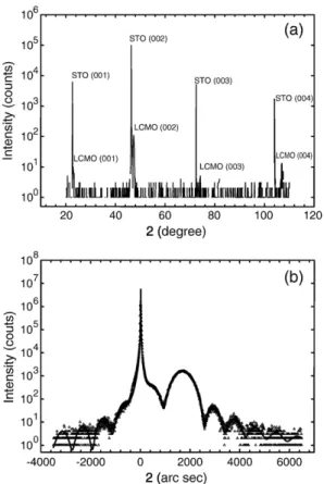
Fig. 1. The X-ray spectra, (a) and (b), of a 21 nm thick La0.67Ca0.3MnO3film.
The c-oriented textured-film exhibits a contracted c-axis due to the strong in-plane strain. The composition and the thickness analysis by the rocking curve analysis dynamical simulation, as shown in (b), give the thickness of the film of 21.3 nm, which is the same as the value of 21 nm estimated by RBS.
Fig. 2. Reciprocal mapping of the (303) peak of the 21 nm La0.67Ca0.3MnO3
within the resolution of equipment accuracy. The thickness was doubly confirmed by RBS and X-ray diffraction spectrum. The possible oxygen depletion for thinner films during growth– which usually causes a lower transition temperature, a higher resistivity [15–17] and an elongating of the c-axis [15]–was
removed by additional in-situ annealing at 850 °C under 6.7 × 10⁴ Pa pure oxygen for 1 to 2 h. With this annealing process, the resistivities of films were lowered dramatically and the c-axes were shortened systematically due to the strong strain effect at the substrate–film interface.
The X-ray diffraction ω–2θ scan, as shown in Fig. 1(a), indicates a texture growth of films with the c-axis perpendicular to the substrate surface. The peak-split analysis of the ω–2θ scan, as shown in Fig. 1(b), gives the c lattice parameter of 0.382 nm, which indicates a strong in-plane strain on the film, resulting in a shortening of the c-axis. The rocking curve anal-ysis dynamical simulation estimates the thickness of the film to be 21.3 nm, which is very close to 21 nm, the value measured by RBS. The epitaxial and strained properties of this film were confirmed by the reciprocal mapping of the (303) peak, as shown inFig. 2. The in-plane lattices for films with various thickness were measured and exhibited similar characteristics as reported previously[10,18]. This in-plane strain makes the a and b lattices expand to 0.391(2) nm and the c lattices contract to 0.382(2) nm. When films become thicker than 25 nm, strain relaxation starts to take place, so that the in-plane and out-plane lattices are gradually restored to the bulk values.
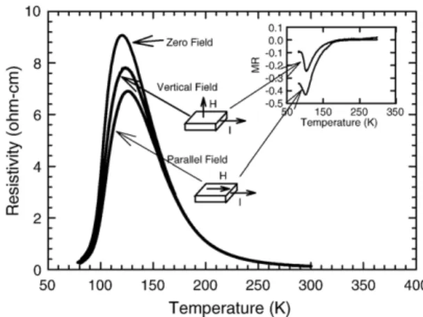
The resistance versus temperature curves for a 21 nm film, as shown inFig. 3, were measured in 0 and 159,000 A m− 1fields along the ab-plane and c-axis. Here the zero-field curve shows a typical metal-insulator like transition at Tpof approximately
121 K. The resistivity at 300 K, 119 mΩ cm, is one order higher than the resistivity, 27 mΩ cm, of a thick film with a transition temperature of 265 K, and is similar to those of the impurity-implanted films [19,20]. The zero-field cooled magnetization measurements at 318,000 A m− 1were investigated by SQUID, as plotted inFig. 4. The ferromagnetic transition temperature Tc
at 318,000 A m− 1is generally higher than Tpat zero-field; for
instance, for the 21 nm film, the Tc(163 K) is higher than Tp
(121 K). This reduction of Tpand Tc, and the increase of
resis-tivity are believed to be due to the in-plane tension in films and to the thickness of films. The thinner the film, the stronger the in-plane strain [5–10] and the more closely it approaches a 2D system. The former factor increases the angle of the Mn–O–Mn bond [21], while the latter one reduces the magnetic coupling indicated by the gradually increasing magnetization to temper-ature curve for the 21 nm film, as shown in the insert ofFig. 4. The combination of these two effects lowers the Tc and Tp.
Furthermore, the TcNTp phenomenon was also observed in
granular samples [14,22], in which the surface phenomenon in the grain-boundary affected the spin tunneling (SPT) effect
[23,24]. However, the SPT effect often produces a low-field MR (LFMR) along a wider temperature range[25,26]. In the inset of
Fig. 3 are the MR curves when the 159,000 A m− 1 file was applied perpendicular or parallel to the surface of the substrate. The MR shows peak configurations that are not consistent with those predicted by SPT; therefore, the existence of the granular effect is less likely in our films.
The LFMR of the 21 nm film at various temperatures, as shown inFig. 5, were measured by applying fields which were vertical or parallel to the substrate surface. They can be divided into two categories: the wide-hysteresis group and the narrow-hysteresis group. According to the conventional domain rota-tion effect and the DE coupling, the magnetic moments of the magnetic domains in films should follow the direction of the high field, while the film should exhibit a low resistivity. When the field decreases to zero, the number of oppositely aligned domains starts to increase, which in turn increases the resis-tivity. When the field is reversed and increases negatively to a critical field, Hc′, the number of oppositely aligned domains
reaches a maximum value and the film exhibits a resistivity peak. Once the applied field is larger than Hc′, domains are
increasing align to the applied field and the resistivity decreases
Fig. 4. The thickness dependence of Tcand Tp. The thinner the film, the stronger
the in-plane strain and the more closely it approaches a 2D system. The Tcis
estimated from the magnetization to temperature (M–T) curves with an applying field of 318,000 A m− 1after cooling at zero magnetic field. The Tpis the
metal-insulator transition temperature measured at zero magnetic field. All M–T curves are plotted in the insert with●, ■, ▴ and ♦ for films with thicknesses of 21, 51, 135 and 190 nm.
Fig. 3. Resistivity to temperature curves of the 21 nm La0.67Ca0.3MnO3film on
the SrTiO3(001) substrate. Curves are measured in zero and in 159,000 A m- 1
magnetic fields that are applied parallel or perpendicular to the substrate. The MRs are calculated from the R–T curves, as shown in the inset. The maximum MR at TMR are −24% and −43% for the parallel and perpendicular
again. It is clear fromFig. 5that, at 77 K, Hc′ is approximately
79,500 A m− 1for the vertical configuration and 7950 A m− 1for the parallel-field configuration. The difference in Hc′ between
these configurations implies the possible anisotropy of the magnetic easy-axis along the c-axis. Therefore, a stronger reverse field is required to flip the magnetic moment. The anisotropic MR is decreasing with the thickness of the films and eventually disappears for the 190 nm film. Intuitively, the critical field, Hc′, in the MR measurement should be the same as
the coercive field, Hc, in the magnetization measurement.
At the critical field, Hc′, both vertical and parallel
configura-tions have a positive MR of approximately + 4.5% and + 3%, respectively. When the applied field is larger than 2Hc′, the
hysteresis loop merges into symmetrically saturated curves. When the field was set at 159,000 A m− 1, a large negative MR was measured. The MR in the parallel configuration, MR(//), is larger than in the vertical configuration, MR(⊥). Surprisingly, the anisotropic constrain along c-axis does not contribute large MR(⊥), as would be expected from the wider hysteresis.
The hysteresis loop of the 21 nm films in vertical and parallel configurations was measured at 77 K as shown in Fig. 6. The magnetization in both configurations exhibits the same initial ramp slope and the saturated magnetization, Ms, which indicates that the
magnetic moment orients itself approximately 45° from the
ab-plane and c-axis. That the coercive fields, Hc∼7950 A m− 1, are
the same in both configurations is consistent with that predicted by the conventional magnetic domain rotation model. Howev-er, at 77 K, the magnetic measurement does not agree with the
MR measurement. As can be clearly seen in Fig. 7(a), by
superimposing the MR and magnetization curves of the vertical configuration at the low field region, the coercivity, Hc(⊥) ∼
7950 A m− 1, and the critical field, Hc′(⊥) ∼ 79,500 A m− 1,
differ by one order of magnitude. Strikingly, this discrepancy is observed only when the applied field is in the vertical
Fig. 6. Magnetization curves at 77 K for fields applied perpendicular and parallel to the substrate.
Fig. 7. Superimposing the magnetoresistance and magnetization curves of the vertical configuration at 77 K. The coercivity field, Hc(⊥)∼7950 A m− 1, and
the critical field, Hc′(⊥)∼79,500 A m− 1where the resistivity peak appears,
differ by one order of magnitude. In the parallel configuration, the coercivity field and the critical field are similar, Hc(//)∼Hc′(//)∼7950 A m− 1.
Fig. 5. Resistivity response to the applied field of the 21 nm film at temperatures above TP(150 K, the metal-insulator transition temperature), at TP(123 K and
126 K for⊥ and // fields), at TM(102 K and 100 K for⊥ and // fields, where the
maximum MR occurred in the R–T measurement when the field was applied at 159,000 A m− 1) and at 77 K.
configuration but not in the parallel configuration, as shown in
Fig. 7(b), where Hc(//)∼ Hc′(//) ∼ 7950 A m− 1. Therefore, the
conventional magnetic domain rotation model does not satisfactorily explain the present results.
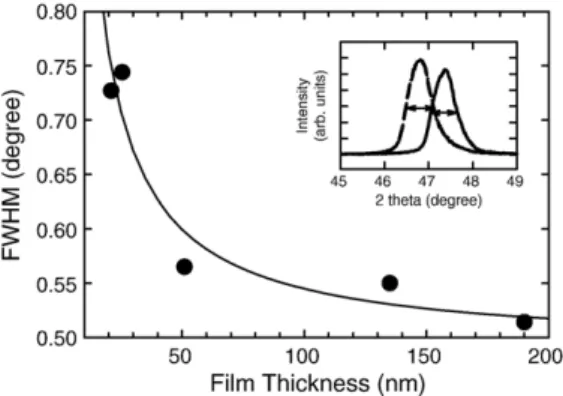
The notably wide FWHM of (200) peaks, taken by a five-axis X-ray diffractometer, for all films, as shown inFig. 8, may be a clue to this discrepancy. Since the lattice distortion in the ab-plane and the c-axis has only a limited effect in peak broadening, the Scherrer formula [27] can act as a semi-quantitative scale for understanding the mechanisms of the peak broadening. Accord-ing to the Scherrer formula, the FWHM along out-plane direction for the 21 nm thick film should be 0.41°. Considering the in-plane direction, roughness might be assumed to have an effect in the FWHM. Yet, due to the fact that the room temperature atomic force microscopy over an area of 25 × 25μm2has shown a very smooth surface with an rms roughness value of 0.679 nm, the FWHM of the in-plane peak should not be affected by the surface roughness and should be much smaller than 0.41°. However, the FWHM of the (200) peak of the 21 nm thick film is 0.73°, which is much wider than that predicted by the Scherrer formula. This implies the existence of some physical nanostructures that divide the film into numerous nano-size domains which stop the con-tinuity of long range crystal lattices. The FWHM for the 21 nm film is large, 0.73°, and then decreases exponentially until it reaches a saturated value of 0.52° for the 190 nm film. The strong similarity between the lattice evolution and the FWHM of the (200) peak versus film thickness indicates that the nanostructure coalesces in thicker films. However, the four-fold symmetry in the phi-scan of the (200) peak of this film indicates that the matrix of the film is basically an epitaxial single crystal film. Therefore, either the matrix may be divided by some physical areas that limit the Bragg construction diffraction, or the matrix has the same phase throughout the entire film with some percentage of the dispersed second phase having lattice constant very similar to the matrix itself.
Possible physical structures such as the columnar morphology in the films may divide the films into different domains or grains that broaden the in-plane peaks. It has been observed that the columnar structure normally appears in thicker films [28], as shown inFig. 9. If the existence of the second phase is responsible
for this inconsistency, then it should have the same composition and very similar crystal structure. The segregation of ferromag-netic clusters in a paramagferromag-netic matrix for CMR materials at temperatures below 1.8Tcis well known in bulk CMR materials
[29,30]. Thus, the ferromagnetic phase could either be segregated in nano- or micron-scale, or in stable or dynamic state, depending on the environment that interacts with it[31]. Because the X-ray diffraction was taken at room temperature nearly 1.8 times the Tc
(163 K) of the 21 nm film, it is highly possible that some nano-scale ferromagnetic clusters are segregated from the paramagnetic matrix. The segregation phase could be stabilized by the strong substrate/film tensile strain at the nano-scale in thinner films. When the film becomes thicker, and the room temperature cor-responds to a temperature closer to Tc, the ferromagnetic clusters
coalesce, therefore growing in size and becoming less in number, thus providing larger physical domains which sharpen the in-plane (200) peak.
With the nanostructures in these films, the boundary effects may alter the direction of whichever Mn moments are close to it and thereby introduce an extra degree of fluctuation to the system. Compared with the bulk grains, this fluctuation has only a limited effect that will not change the total moment. However, it does affect the hopping of carriers across the boundaries. Because the boundaries are all perpendicular to the surface of the film, they cause different transport behaviors for vertical and parallel configurations.
4. Conclusion
Here we have reported inconsistent MR and magnetic properties of LCMO thin films grown on STO (001) substrate by off-axis radio frequency sputtering, properties which cannot be understood by the conventional domain rotation model alone. Nanostructures in the film may be responsible for the discrepancy between the magnetic and transport measurements under a vertical magnetic field.
Acknowledgment
We would like to acknowledge Professor H.D. Yang and M.-H. Tsai for their advice. This study was supported by the National
Fig. 9. The cross-section TEM image of the 300 nm film indicates a high density of columnar structure.
Fig. 8. The FWHM of X-ray (200) diffraction peaks as a function of the film thickness. The standardω–2θ scan of (200) peaks for 21 and 190 nm thick films are plotted as the solid and dashed lines, respectively, in the insert where the change of peak width and position are obvious.
Science Council of Taiwan under Grant No. NSC-93-2112-M110-017.
References
[1] C. Zener, Phys. Rev. 82 (1951) 403.
[2] P.W. Anderson, H. Hasegawa, Phys. Rev. 100 (1955) 675. [3] P.G. deGennes, Phys. Rev. 118 (1960) 141.
[4] A.J. Millis, P.B. Littlewood, B.I. Shraiman, Phys. Rev. Lett. 74 (1995) 5144.
[5] S. Jin, T.H. Tiefel, M. McCormack, H.M. O'Bryan, L.H. Chen, R. Ramesh, D. Schurig, Appl. Phys. Lett. 67 (1995) 557.
[6] Y. Suzuki, H.Y. Hwang, S.-.W. Cheong, R.B. VanDover, Appl. Phys. Lett. 71 (1997) 140.
[7] J. O'Donnell, M.S. Rzchowske, J.N. Eckstein, I. Bozovic, Appl. Phys. Lett. 72 (1998) 1775.
[8] S. Freisem, A. Brockhoff, D.G. de Groot, B. Dam, J. Arats, J. Magn. Magn. Mater. 165 (1997) 380.
[9] E. Gommert, H. Cerva, J. Wecker, K. Samwer, J. Appl. Phys. 85 (1999) 5417.
[10] R.A. Rao, D. Lavric, T.K. Nath, C.B. Eom, L. Wu, F. Tsui, J. Appl. Phys. 85 (1999) 4744.
[11] F. Tsui, M.C. Smoak, T.K. Nath, C.B. Eom, Appl. Phys. Lett. 76 (2000) 2421.
[12] B. Vengalis, A. Maneikis, F. Anisimovas, R. Butkute, L. Dapkus, A. Kindurys, J. Magn. Magn. Mater. 211 (2000) 35.
[13] J. O'Donnell, M. Onellion, M.S. Rzchowski, J.N. Eckstein, I. Bozovic, Phys. Rev., B 54 (1996) R6841.
[14] Y. Fu, Appl. Phys. Lett. 77 (2000) 118.
[15] M. Rajeswari, R. Shreekala, A. Goyal, S.E. Lofland, S.M. Bhagat, K. Ghosh, R.P. Sharma, R.L. Greene, R. Ramesh, T. Venkatesan, Appl. Phys. Lett. 73 (1998) 2672.
[16] A. Goyal, M. Rajeswari, R. Shreekala, S.E. Lofland, S.M. Bhagat, T. Boettcher, C. Kwon, R. Ramesh, T. Venkatesan, Appl. Phys. Lett. 71 (1997) 2535.
[17] H.L. Ju, J. Gopalakrishnan, J.L. Peng, Q. Li, G.C. Xiong, T. Venkatesan, R.L. Greene, Phys. Rev., B 51 (1995) 6143.
[18] M. Ziese, H.C. Semmelhack, K.H. Han, S.P. Sena, H.J. Blythe, Appl. Phys. 91 (2002) 9930.
[19] C.-H. Chen, V. Talyansky, C. Kwon, M. Rajeswari, P. Sharma, R. Ramesh, T. Venkatesan, J. Melngailis, Z. Zhang, W.K. Chu, Appl. Phys. Lett. 69 (1996) 3089.
[20] V.M. Browning, R.M. Stroud, W.W. Fuller-Mora, J.M. Byers, M.S. Ososfsky, D.L. Knies, K.S. Grabowski, D. Koller, J. Kim, D.B. Chrisey, J.S. Horwitz, J. Appl. Phys. 83 (1998) 7070.
[21] A. Miniotas, A. Vailionis, E.B. Svedberg, U.O. Karlsson, J. Appl. Phys. 89 (2001) 2134.
[22] L. Zheng, K. Li, Y. Zhang, Phys. Rev., B 58 (1998) 8613. [23] J. Inoue, J. Phys. D. Appl. Phys. 31 (1998) 643. [24] F. Guinea, Phys. Rev., B 58 (1998) 9212.
[25] Y. Lu, X.W. Li, G.Q. Gong, G. Xiao, A. Gupta, P. Lecoeur, J.Z. Sun, Y.Y. Wang, V.P. Dravid, Phys. Rev., B 54 (1996) 8357.
[26] N.D. Mathur, G. Burnell, S.P. Isaac, T.J. Jackson, B.S. Teo, J.L. Mac Manus-Driscoll, L.F. Cohen, J.E. Evetts, M.G. Blamire, Nature 387 (1996) 266.
[27] B.D. Cullity, Elements of X-ray Diffraction, Mass, 2nd edition, Addison-Wesley, 1978, p. 102.
[28] E. Gommert, H. Cerva, A. Rucki, R.V. Helmolt, J. Wecker, C. Kuhrt, K. Samwer, J. Appl. Phys. 81 (1997) 5496.
[29] J. Goodenough, J.-S. Zhou, Nature 386 (1997) 229.
[30] J.M. De Tereasa, M.R. Ibarra, P.A. Algarabel, C. Ritter, C. Marquina, J. Blasco, J. Garcia, A. del Moral, Z. Arnold, Nature 386 (1997) 256. [31] T. Kanki, R.W. Li, Y. Naitoh, H. Tanaka, T. Matsumoto, T. Kawai, Appl.