Room-temperature-operated sensitive hybrid gas sensor based on amorphous
indium gallium zinc oxide thin-film transistors
Hsiao-Wen Zan, Chang-Hung Li, Chun-Cheng Yeh, Ming-Zhi Dai, Hsin-Fei Meng, and Chuang-Chuang Tsai
Citation: Applied Physics Letters 98, 253503 (2011); doi: 10.1063/1.3601488
View online: http://dx.doi.org/10.1063/1.3601488
View Table of Contents: http://scitation.aip.org/content/aip/journal/apl/98/25?ver=pdfcov Published by the AIP Publishing
Articles you may be interested in
Threshold voltage dependence on channel length in amorphous-indium-gallium-zinc-oxide thin-film transistors Appl. Phys. Lett. 102, 083508 (2013); 10.1063/1.4793996
Environment-dependent thermal instability of sol-gel derived amorphous indium-gallium-zinc-oxide thin film transistors
Appl. Phys. Lett. 98, 152109 (2011); 10.1063/1.3580614
Light induced instabilities in amorphous indium–gallium–zinc–oxide thin-film transistors Appl. Phys. Lett. 97, 173506 (2010); 10.1063/1.3503971
Organic/inorganic hybrid complementary circuits based on pentacene and amorphous indium gallium zinc oxide transistors
Appl. Phys. Lett. 93, 213505 (2008); 10.1063/1.3039779
High-performance amorphous gallium indium zinc oxide thin-film transistors through N 2 O plasma passivation
Appl. Phys. Lett. 93, 053505 (2008); 10.1063/1.2962985
This article is copyrighted as indicated in the article. Reuse of AIP content is subject to the terms at: http://scitation.aip.org/termsconditions. Downloaded to IP: 140.113.38.11 On: Wed, 30 Apr 2014 09:04:33
Room-temperature-operated sensitive hybrid gas sensor based
on amorphous indium gallium zinc oxide thin-film transistors
Hsiao-Wen Zan,1,a兲 Chang-Hung Li,1Chun-Cheng Yeh,1Ming-Zhi Dai,2Hsin-Fei Meng,2 and Chuang-Chuang Tsai1
1
Department of Photonic, Institute of Electro-Optical Engineering, National Chiao Tung University, Hsinchu 300, Taiwan
2
Institute of Physics, National Chiao Tung University, 1001, Ta Hsueh Road, Hsinchu 300, Taiwan
共Received 18 April 2011; accepted 28 May 2011; published online 22 June 2011兲
An organic sensing layer is capped onto an amorphous indium gallium zinc oxide 共a-IGZO兲 thin-film transistor共TFT兲 to form a hybrid sensor. The organic layer, served as a second gate, forms a p-n junction with the a-IGZO film. Oxidizing or reducing vapor molecules act like electron acceptors or electron donors to change the potential of the organic layer and the current of a-IGZO TFT. A sensitive and reversible response to 100 ppb ammonia and 100 ppb acetone is obtained at room temperature. This letter opens a route to develop low-cost large-area bio/chemical sensor arrays based on the emerging a-IGZO TFT technology. © 2011 American Institute of Physics. 关doi:10.1063/1.3601488兴
With a high mobility 共⬎10 cm2/V s兲, a low threshold voltage 共⬍5 V兲, a high on/off ratio, high uniformity over large area, and process availability at room temperature, amorphous indium gallium zinc oxide thin-film transistors 共a-IGZO TFTs兲 have attracted much attention since they were first reported by Hosono and co-workers.1 Recently, a-IGZO TFTs have been used as the pixel switching or driv-ing circuits in active-matrix liquid crystal displays and active-matrix organic-light-emitting-diode displays.2,3In this letter, we propose a sensitive vapor sensor based on conven-tional a-IGZO TFT. Sensitive vapor sensors are important for the development of noninvasive diagnostic breath analy-sis system.4–6 For example, the breath NH3 concentration is
higher in patients with liver diseases or disturbed urea bal-ance 共⬃0.7 ppm兲 than that in normal person 共⬍0.3 ppm兲.4 Patients with diabetes exhale higher concentration of acetone than normal persons.5Nitric oxide共NO兲 gas sensor is impor-tant for asthma attack prevention.6
However, high sensitivity 共⬍1 ppm兲 is obtained only when nanostructure is used to increase the surface to volume ratio and the sensors are operated at an elevated temperature 共e.g., ⬎200 °C兲.7,8
In this letter, instead of utilizing the re-action between the vapor molecules and the metal-oxide semiconductor material, an organic sensing layer 共OSL兲 is capped onto a conventional bottom-gate top-contact a-IGZO TFT to form a hybrid sensor. The organic layer and the a-IGZO film form a p-n junction. Oxidizing or reducing va-por molecules act like electron acceptors or electron donors to change the potential of the OSL and thus change the en-ergy band equilibrium of the p-n junction. As a result, the current of a-IGZO TFT is significantly changed. The pro-posed mechanism has been utilized to form a sensitive vis-ible light sensor in our previous report.9In that work, visible light absorbed by the organic capping layer produces electron–hole pair, injects electrons into a-IGZO film, and changes the TFT threshold voltage. In another work, we capped various kinds of metals onto the back interface of a-IGZO TFT. The built-in potential between the floating
cap-ping metal and a-IGZO is utilized to adjust the device threshold voltage. The capping layer is served as a floating second gate to influence the characteristics of a-IGZO TFT.10 In this letter, two kinds of organic materials 关poly共3-hexylthiophene兲 共P3HT兲 and copper phthalocyanine 共CuPc兲兴 are used as the gas sensing layers. The P3HT-capped hybrid sensor and CuPC-capped hybrid sensor exhibit a fast and reversible response to 100 ppb ammonia and 100 ppb ac-etone, respectively. A gate bias modulated sensitivity is in-vestigated. Opposite responses to electron donors 共ammonia and acetone兲 and electron acceptor 共NO兲 are clearly ob-served.
First, standard共STD兲 a-IGZO TFTs were fabricated with experimental conditions described in our previous report9 while the channel length and width were changed to be 200 m and 1000 m, respectively. For P3HT-capped de-vices, P3HT共RR⬎98.5%, Rieke Metals Inc.兲 derived from chlorobenzene 共1.5 wt %兲 was coated on some STD devices in 7000 rpm; the coated devices were then annealed at 200 ° C for 10 min. The thickness of the P3HT film was 20 nm. For CuPC-capped devices, a 50-nm-thick CuPc 共purity ⬎99%, Lumtec兲 was deposited on the STD device by ther-mal evaporation at room temperature with a deposition rate as 0.5 Å/s under 2⫻10−6 torr. The threshold voltage and
mobility were determined from the slope and the x-axis in-tercept of the transfer characteristics measured under satura-tion condisatura-tion共VDS=20 V; VGSwas varied from⫺15 to 20
V兲. To investigate the gas sensing response, devices were put in a microfluid sensing chamber and the background ambient is kept as high purity 99.9999%兲 nitrogen 共N2兲. We used the
electrical syringe pump system to inject the test gas共acetone with a purity as 99.999% and NH3 with a purity as 99.9999%兲 into a tube to blend with N2completely and then
the mixed gas enters the microfluid system. The amount of N2was controlled by a mass-flow controller and the specific
concentration of test gas was attained by adjusting the injec-tion speed of electrical syringe pump. The concentrainjec-tion of NO gas was controlled by a mass-flow controller.
The schematic diagram of organic-capped a-IGZO TFT is shown in Fig.1共a兲. When the OSL is exposed to oxidizing or reducing gases, the potential of the OSL is changed. Since a兲Author to whom correspondence should be addressed. Electronic mail:
APPLIED PHYSICS LETTERS 98, 253503共2011兲
0003-6951/2011/98共25兲/253503/3/$30.00 98, 253503-1 © 2011 American Institute of Physics
This article is copyrighted as indicated in the article. Reuse of AIP content is subject to the terms at: http://scitation.aip.org/termsconditions. Downloaded to IP: 140.113.38.11 On: Wed, 30 Apr 2014 09:04:33
the OSL is treated as a floating second gate, the potential variation in the OSL significantly influences the current of the a-IGZO TFT.
Initial transfer characteristics of STD device, P3HT-capped device, and CuPC-P3HT-capped device are shown in Fig. 1共b兲. The field-effect mobilities 共FE兲, threshold
volt-ages 共VTH兲, subthreshold swings 共S.S.兲, and on/off ratio of
STD device are 13.8 cm2/V s, 0.72 V, 0.19 V/dec, and 2.9
⫻106, respectively. For P3HT-capped device, they are
10.7 cm2/V s, 1.4 V, 0.28 V/dec, and 2.2⫻106. For CuPC-capped device, they are 13.3 cm2/V s, 1.33 V, 0.27 V/dec,
and 1.0⫻107. Obviously, capping organic semiconductor
onto a-IGZO TFTs does not cause significant influences on basic device characteristics.
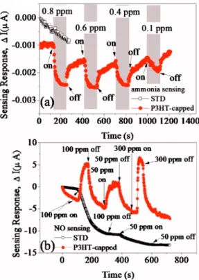
Then, the responses of STD a-IGZO TFT and P3HT-capped a-IGZO TFT to ammonia are investigated. Drain cur-rent variations 共⌬I兲 in these two devices are plotted as a function of time exposed to different ammonia concentration in Fig. 2共a兲. Devices are biased at VGS− VTH= 0.3 V and
VDS= 1 V. For STD device, no significant response can be
observed when ammonia concentration is 10 or 0.8 ppm. For P3HT-capped device, an obvious current drop is obtained when device is exposed to ammonia. After the removal of ammonia, the current drop is recovered. The ammonia sens-ing response of a P3HT-based organic TFT has been reported with ammonia concentration ranging from 10 to 100 ppm.11 In that report, ammonia molecules behave as acceptorlike deep trap states共or as electron donors兲 to trap the holes at the P3HT/dielectric interface, shift the threshold voltage to be more negative and cause a current drop. In our study, a posi-tive threshold voltage shift is observed when device is ex-posed to ammonia 共not shown兲. Ammonia molecules ab-sorbed onto P3HT act like reducing agents to inject electrons into P3HT. The negative potential on P3HT layer, the second gate, shifts the threshold voltage to be more positive and
produces a current drop in a-IGZO TFT. The sensing sensi-tivity is high because the threshold voltage is sensitive to the body potential. In our letter, a clear response to 0.1 ppm ammonia is observed. The sensing sensitivity is also strongly influenced by the thickness of P3HT.
To further verify the aforementioned mechanism, a typi-cal oxidizing gas, NO, is used to stimulate the P3HT-capped device. Drain current variations 共⌬I兲 in STD device and of P3HT-capped device are plotted as a function of time ex-posed to different NO concentration in Fig.2共b兲. Devices are biased at VGS− VTH= 8.6 V and VDS= 20 V. When STD
de-vice is exposed to NO gas, a slow current drop is observed. The current drop is not able to be recovered even when NO is removed. The slow and irreversible response is due to the slow adsorption and desorption of NO molecules on the ox-ide semiconductor thin film.6 When P3HT-capped a-IGZO TFT is exposed to NO, on the contrary, a fast current in-crease is observed. A fast recovery behavior is also obtained when NO is removed. The P3HT capping blocks the reaction between NO and a-IGZO film. The sensing behavior is dominated by the reaction between NO and P3HT in which NO molecules act as oxidizing agents to withdraw electrons from P3HT.12 The positive potential on P3HT film helps to turn on the transistor and thus increase the current of a-IGZO TFT.
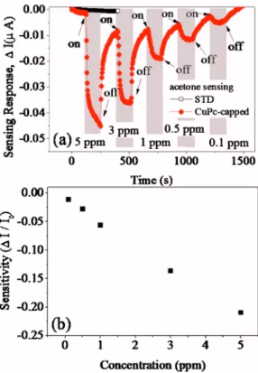
Metal phthalocyanine thin films are also known to be good gas sensors because their electronic properties are af-fected by the adsorption of oxidization or reducing gas.13In the following section, CuPc is capped onto the back channel of a-IGZO TFT to detect a kind of reducing gas, acetone, which is an index gas in the breath of patients with metabolic disease such as diabetes mellitus.5 Drain current variations 共⌬I兲 in STD device and CuPC-capped device are plotted as a function of time exposed to different acetone concentration FIG. 1. 共Color online兲 共a兲 Schematic diagram of organic-capped a-IGZO
TFT and 共b兲 transfer characteristics of STD, P3HT-capped, and CuPC-capped device measured at VDS= 20 V.
FIG. 2. 共Color online兲 Drain current variation 共⌬I兲 in STD and P3HT-capped device as a function of time exposed to different concentration of 共a兲 ammonia at VGS− VTH= 0.3 V, VDS= 1 V and 共b兲 NO at VGS− VTH
= 8.6 V, VDS= 20 V.
253503-2 Zan et al. Appl. Phys. Lett. 98, 253503共2011兲
This article is copyrighted as indicated in the article. Reuse of AIP content is subject to the terms at: http://scitation.aip.org/termsconditions. Downloaded to IP: 140.113.38.11 On: Wed, 30 Apr 2014 09:04:33
in Fig. 3共a兲. Devices are biased at VGS− VTH= 0.5 V and
VDS= 1 V. For STD device, no clear response to acetone can
be observed, indicating a weak charge transfer interaction between the a-IGZO and acetone at room temperature. For CuPC-capped a-IGZO TFT, on the contrary, a fast, sensitive, and reversible response to acetone is obtained. The sensitiv-ity 共i.e., the response current variation ratio, ⌬I/I0, when sensing time is fixed as 120 s兲 is plotted as a function of acetone concentration in Fig. 3共b兲. A linear relationship is observed. The sensing sensitivity is as high as 100 ppb and is promising to be used to distinguish healthy humans 共ⱕ900 ppb兲 and diabetes patients 共ⱖ1800 ppb兲. For P3HT-capped device, a linear relationship is also observed when the response current variation ratio is plotted as a function of ammonia concentration共not shown兲.
An interesting gate-bias-dependent sensing sensitivity is also found. As shown in Fig. 4, the current variation ratio 共⌬I/I0兲 is plotted as a function of time when devices are
exposed to 5 ppm acetone and recovered in pure nitrogen under different bias condition. When VGS− VTH= 5 V and
VDS= 1 V, ⌬I/I0 is less than 0.04 and is similar to⌬I/I0of
the floating gate condition, implying that the sensing mecha-nism is similar to a chemical resistor rather than a chemical transistor. When VGS− VTH= 0.5 V and VDS= 1 V, ⌬I/I0 is
improved 5.5 times and reaches 0.22. The gate-bias-dependent sensitivity can be explained as follows. When VGS
is large, the channel carriers are mostly induced and con-trolled by VGS. The potential variation in the OSL共i.e., the
second gate兲 caused by the charge transfer between acetone and the OSL is much smaller than VGS. Thus, the channel
current has only a weak response to the acetone molecules. When VGS− VTH= 0.5 V, the potential variation in the OSL
is comparable to VGS− VTH. The channel current is then
sig-nificantly influenced by the charge transfer between the OSL and gas molecules.
In this letter, we demonstrated a sensitive gas sensor based on a hybrid organic/inorganic TFT. The OSL is capped onto the back channel of a conventional bottom-gate top-contact a-IGZO TFT. When the sensing layer top-contacts with oxidizing or reducing gas molecules, charge transfer between the sensing layer and the gas molecules changes the potential of the sensing layer. The variation in the sensing layer po-tential can be detected by the underlying a-IGZO TFT since the sensing layer is served as a floating second gate. The organic semiconductor material easily reacts with bio/ chemical molecules to cause the charge transfer. The charge transfer is then amplified by the underlying transistor and the sensing current is delivered by the channel in a-IGZO film with high electron mobility. The demonstrated sensitivity to 100 ppb acetone and 100 ppb ammonia enables the device to be developed for noninvasive diagnostic of patients with dia-betes or liver diseases.
This work was supported in part by the National Science Council under Grant NSC-99–2627–B-009–006 and in part by Veterans General Hospitals University System of Taiwan Joint Research Program under Grant VGHUST100–G5–1–3. 1K. Nomura, H. Ohta, A. Takagi, T. Kamiya, M. Hirano, and H. Hosono,
Nature共London兲 432, 488共2004兲.
2H. H. Hsieh, H. H. Lu, H. C. Ting, C. S. Chuang, C. Y. Chen, and Y. Lin, J. Soc. Inf. Disp. 11, 160共2010兲.
3J. S. Park, T. W. Kim, D. Stryakhilev, J. S. Lee, S. G. An, Y. S. Pyo, D. B. Lee, Y. G. Mo, D. U. Jin, and H. K. Chung,Appl. Phys. Lett. 95, 013503
共2009兲.
4C. Shimamoto, I. Hirata, and K. Katsu, Hepato-Gastroenterology 47, 443 共2000兲.
5M. Righettoni, A. Tricoli, and S. E. Pratsinis, Anal. Chem. 82, 3581 共2010兲.
6C. C. Liu, J. H. Li, C. C. Chang, Y. C. Chao, H. F. Meng, S. F. Horng, C. H. Hung, and T. C. Meng,J. Phys. D: Appl. Phys. 42, 155105共2009兲.
7Q. Qi, T. Zhang, L. Liu, X. Zheng, Q. Yu, Y. Zeng, and H. Yang,Sens. Actuators B 134, 166共2008兲.
8J. Shi, G. Hu, Y. Sun, M. Geng, J. Wu, Y. Liu, M. Ge, J. Tao, M. Cao, and N. Dai,Sens. Actuators B 156, 820共2011兲.
9H. W. Zan, W. T. Chen, H. W. Hsueh, S. C. Kao, M. C. Ku, C. C. Tsai, and H. F. Meng,Appl. Phys. Lett. 97, 203506共2010兲.
10H. W. Zan, W. T. Chen, C. C. Yeh, H. W. Hsueh, C. C. Tsai, and H. F. Meng,Appl. Phys. Lett. 98, 153506共2011兲.
11J. W. Jeong, Y. D. Leea, Y. M. Kima, Y. W. Parka, J. H. Choia, T. H. Parka, C. D. Soob, S. M. Wonb, I. K. Hanc, and B. K. Jua,Sens. Actuators B 146, 40共2010兲.
12V. Saxena, D. K. Aswal, M. Kaur, S. P. Koiry, S. K. Gupta, J. V. Yakhmi, R. J. Kshirsagar, and S. K. Deshpande, Appl. Phys. Lett. 90, 043516
共2007兲.
13G. Guillaud, J. Simon, and J. P. Germain,Coord. Chem. Rev. 178–180, 1433共1998兲.
FIG. 3. 共Color online兲 共a兲 Drain current variations 共⌬I兲 in STD and CuPc-capped device as a function of time exposed to acetone with different con-centration at VGS− VTH= 0.5 V and VDS= 1 V,共b兲 the sensitivity 共i.e., the
current variation ratio,⌬I/I0兲 of CuPc-capped device as a function of ac-etone concentration. Bias conditions: VGS− VTH= 0.5 V and VDS= 1 V.
FIG. 4. 共Color online兲 The sensitivity of CuPc-capped device as a function of time exposed to 5 ppm acetone at VDS= 1 V with different VGS− VTH.
253503-3 Zan et al. Appl. Phys. Lett. 98, 253503共2011兲
This article is copyrighted as indicated in the article. Reuse of AIP content is subject to the terms at: http://scitation.aip.org/termsconditions. Downloaded to IP: 140.113.38.11 On: Wed, 30 Apr 2014 09:04:33