Ultrathin Oriented BiFeO
3
Films from Deposition of Atomic Layers
with Greatly Improved Leakage and Ferroelectric Properties
Yen-Ting Liu,
†Ching-Shun Ku,*
,‡Shang-Jui Chiu,
‡Hsin-Yi Lee,*
,‡,§and San-Yuan Chen
§‡National Synchrotron Radiation Research Center, Hsinchu 30076, Taiwan
†Program for Science and Technology of Accelerator Light Source and§Department of Materials Science and Engineering, National
Chiao Tung University, Hsinchu 30010, Taiwan
ABSTRACT: Highly (001)-oriented BiFeO3ultrathinfilms of total thickness of less than
10 nm were deposited on Si(001) substrates via deposition of atomic layers (ALD) with a LaNiO3 buffer. A radio-frequency (RF)-sputtered sample of the same thickness was
prepared for comparison. The ALD combined with interrupted flow and an exchange reaction between Bi and Fe precursors provides a superior method to grow ternary compounds. According to X-ray diffraction, upon deposition at a temperature of less than 550°C, the only phase in the film was BiFeO3. Anomalousfine structure from synchrotron
X-ray diffraction certified the valence bonding through the BiFeO3(001) diffraction signal. The stoichiometric ratio of BiFeO3 obtained from X-ray photoelectron spectroscopy
indicated that ALD has a proportion much improved over the RF preparation, and this is also in agreement with the results for diffraction anomalous fine structure. The use of high-resolution transmission electron and atomic force microscopes showed that the layer structure and morphology from ALD presented a satisfactory coverage, more conformal than that with the RF method. The BiFeO3thinfilm deposited with ALD shows excellent
leakage, improved at least 1000 times with respect to the RF preparation, making this method suitable for the fabrication of ferroelectric random-access memory devices. From the hysteresis loop, the largest remanent polarization was observed as 2Pr= 2.0μC cm−2.
KEYWORDS: BiFeO3, atomic layer deposition
■
INTRODUCTIONMultiferroic oxide BiFeO3 (BFO) has been investigated for many years. Since Wang et al.1reported a major discovery of heterostructure epitaxial BFO, many publications have appeared that demonstrate diverse techniques for the growth of BFO thin films, such as pulsed-laser deposition (PLD), radio-frequency magnetron sputtering (RF-sputtering), sol−gel, chemical vapor deposition (CVD), and electrophoretic deposition.2Their authors illustrated and dissected the physical properties and crystal quality.3−8The reasons that BFO attracts so much attention are its superior ferroelectric properties as a thin film and the coexistence of ferroelectric and magnetic ordering.8Both the Curie (TC∼ 1100 K) and Neel (TN∼ 673
K) temperatures are well above room temperature (RT), and BFO exhibits a long-range coupling of the electric and magnetic degrees of freedom at RT3,9−11 that enables it to be used reliably in a real environment. BFO shows advantages as a medium for information storage, which could simplify operation of the present device structures or provide a new architecture.12,13 Moreover, BFO shows an environmental convenience better than that of other lead-based perovskite compounds.
In commercial devices, ferroelectric random-access memories (FRAMs) represent the current state of the art of electro-ceramics, but many other future designs of integrated circuits (ICs) might benefit from electroceramics. To fulfill the
requirements of the semiconductor industry and to introduce a multiferroic material into this field for a new generation of FRAM,9growing a thin layer onto a wafer scale and conformal coverage with small leakage properties for devices are urgent requirements. The development of new and improved methods to process thin films such as atomic-layer deposition (ALD) supports these kinds of applications.
In this report, we introduce ALD for the growth of a BFO thinfilm. ALD is a self-limiting process to grow thin films that possess several practical advantages, including simple and accurate control of thefilm thickness, large area and large batch capability, effective conformality, and reproducibility.14 The conventional ALD process is highly suitable for the growth of binary compounds; only a few reports are published about ternary compounds with ALD,15−17 among which BFO is absent. The most straightforward approach for ALD of multicomponent oxides is to use separate binary deposition cycles and to adjust the composition with variation of the cycle ratio.18All cation precursors must be compatible, i.e., volatile, thermally stable, and reactive at the same process temperature. These requirements yield a fairly narrow process window, which is just below the decomposition temperature of the least
Received: October 12, 2013 Accepted: December 2, 2013 Published: December 2, 2013
stable precursor. The bilayer structure of two binary compounds that are not true ternary compounds is due to poor valence bonding between two cation atoms when the bilayer ratio is large.18 For the purpose of preparing a real ternary BFO, an ultrarapid ALD diaphragm valve installed between the reactor and pump was implemented in a novel ALD process, with interruption of the flow rate. To retain a precursor in the reactor chamber, the valve is closedfirst for a small interval before a precursor is introduced into the reactor.19The main influences of this step are to enhance the precursor density in the reactor and to extend the duration of the reaction at the sample surface, which provides a satisfactory condition to grow a thinfilm.
In this work, we report for the first time a highly (001)-oriented BFO thinfilm grown with ALD on a Si(100) substrate with a LaNiO3 (LNO) buffer layer and a deposition
temperature in the range 480−550 °C, which shows satisfactory results for the crystal structure and ferroelectric properties. We used a LNO buffer layer because it is metallic and can serve both as the bottom electrode in fabricating integrated ferroelectric capacitors on silicon and as an effective interface for the growth of highly textured ferroelectric thinfilms.20−22
■
EXPERIMENTSALD involves a self-limiting vapor-phase chemisorption that relies on consecutive surface reactions and utilizes critical purging steps to prevent interactions between reactive precursors.23 The BFO thin films were grown on a LNO-coated Si(001) substrate using ALD; trimethylbismuth [(CH3)3Bi; purity 95% min; Nanjing Chemlin Chemical Industry Co., Ltd.], cyclohexadieneiron tricarbonyl [C6H8Fe(CO)3; purity 97% min; Alfa Aesar], and deionized water (H2O) served as precursors for atoms of Bi, Fe, and O, respectively. Thinfilms of BFO were deposited to a desired thickness of ∼10 nm. A LNO buffer layer of thickness 50−70 nm was deposited on a Si(001) substrate at 500°C with a RF-sputtering system, which provided a satisfactory condition for the growth of BFO.24
The crystal structure and rate of growth of BFO were determined with standard two-circle X-ray diffraction (XRD) and X-ray reflectometry (XRR). Diffraction anomalous fine structure (DAFS) was measured with a synchrotron source at wiggler beamline BL-17B1 with an eight-circle diffractometer in the National Synchrotron Radiation Research Center in Taiwan. The chemical composition of the BiFeO3 thin film was measured with X-ray photoelectron spectroscopy (XPS; PHI 1600) at a pressure of 10−10Torr and an X-ray energy of 1253.6 eV.
The layer structure and interface roughness of the thin film were investigated with cross-sectional images from high-resolution trans-mission electron microscopy (HRTEM; JEOL JEM2010). The surface morphology was measured by atomic force microscopy (AFM; NT-MDT solver P47H) operating in tapping mode; the scan rate of the tip was kept constant at 0.5 Hz, the scanning lines were numbered 512, and the scan size was set at 2× 2 μm2. The polarization−electric field hysteresis loop and the current density−electric field curve were measured at RT with a ferroelectric test system (TF Analyzer 2000 FE-Module, axiACCT Co.).
■
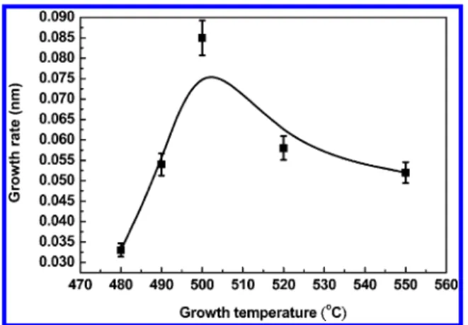
RESULTS AND DISCUSSIONThe rate of deposition of our BFO thinfilms was determined with XRR as a function of the growth temperature, as shown in Figure 1. The rate of growth of BFO increases with the substrate temperature, attaining a maximum value at 500 °C and decreasing with further increased temperature. The phase of BFO is classified as a rhombohedral, distorted, simple-perovskite structure belonging to space group R3c at RT; the perovskite-type unit cell has a pseudocubic lattice parameter a = 0.396 nm.25,26For ALD growth in practice, a water precursor is
introduced into the chamber to form hydroxyl groups in the same plane. From a point of view along the (111) direction of BFO, four O atom planes form a unit cell, and ion or Bi atoms fill in between the two planes of O atoms, but the direction of growth of BFO along the surface was (001) because of a substrate effect. The theoretical rate of deposition of one unit cell would be a quarter of the lattice parameter (0.099 nm cycle−1), which was near our experimental measurement at 0.087 nm cycle−1at 500°C. The growth window of a BFO thin film with the ALD system was narrow, from 490 to 520 °C. Herein, a unique ALD process was adopted to grow a thinfilm of BFO as a truly ternary compound in terms of precursors O, Fe, and Bi to form one ALD cycle; the durations of pulses for O, Fe, and Bi were 100, 400, and 15 ms, respectively. Between the precursor pulse and evacuation of the chamber, the ALD valve was closed to maintain the precursor at a constant vapor pressure in the chamber to increase the duration of the reaction, which we call the“stock time”;14,19for O, Fe, and Bi, these durations were 2, 4, and 0.5 s, respectively. After the stock time, highly pure N2(99.9995 %) gas was employed to purge
the chamber for 5 s at 1.1 Torr and evacuated with a rotary pump for 7 s to a base pressure of 3× 10⁻²Torr before the next precursor was admitted to the chamber, as shown in Figure 2.
Figure 3 shows XRD patterns measured in a radial scan (θ− 2θ scan) along the surface normal of Si(001) at varied temperatures of growth of BFO. At afirst glance, the position of the reflection of BFO (001) is near that of LNO (001), but the integrated intensity of that reflection increased and shifted
Figure 1.Timetable of modified ALD processes for BFO thin film growth.
Figure 2. Rate of ALD growth as a function of the substrate temperature for BFO thinfilms deposited on a LNO-coated silicon substrate.
to a smaller angle, with the deposition temperature increasing from 480 to 500°C, and shows the BFO phase with a preferred orientation along (001). The rocking-curve measurement of the BFO (001) reflection is shown in the inset of Figure 3; the full width at half-maximum of the rocking curve of the BFO (001) reflection is about 5°. A BiFeO3(111) reflection contributes the
diffraction feature observed of about 38−39° for 490−520 °C; this orientation of the thin film is minor. The integrated intensity ratio of the reflections for BFO (111)/(001) was 0.04%, which indicates that the properties of the thinfilm were mostly contributed from the BFO (001) grains. When the temperature was increased to 520 °C, the Bi2O3 (111)
reflection appeared and was accompanied with a decreased intensity of BFO (001). The reason is that a higher temperature of deposition might cause decomposition or degradation of the least stable precursor, cyclohexadieneiron tricarbonyl, so that it no longer becomes reactive with hydroxyl for the formation of BFO. Furthermore, a lower temperature cannot provide sufficient energy to grow a BFO crystal of high quality. With higher or lower temperatures of deposition, the intensity of the diffraction decreased rapidly; these results signify an optimum temperature for growth with the nearest rate of growth of BFO of about 500°C.
In general, X-ray scattering provides information about only the long-range ordering of an atomic structure, but measure-ments of X-ray absorption fine structure (XAFS) provide information about the short-range chemical structure. DAFS combines all capabilities of XRD and XAFS into a single technique: it provides the advantages of information about short-range order above a set or subset of long-range-ordered atoms selected with the diffraction condition.27 DAFS is chemically and valence specific and is sensitive to the positions of neighboring atoms; atoms can be separated by measuring the DAFS intensities of the Bragg peaks with varied contributions to the diffraction structure factor. DAFS provides the same structural and spectral sensitivities as X-ray absorption near-edge structure: the valence, empty-orbital, and bonding information for the resonant atoms.28,29 To indicate the valence states of the Fe and Bi elements, we present the DAFS results of a BFO thinfilm deposited at 500 °C and made on a BFO (001) diffraction line, as shown in Figure 4a,b. The theoretical values of the absorption edges were located at 7.112 keV (K-edge) for Fe atoms and 13.419 keV (L3-edge) for Bi atoms. The experimental results show strong absorption signals of both Fe and Bi atoms at the maxima of the signal energies, 7.115 and 13.422 keV, respectively. This shift is due to Fe and
Bi being present as trivalent ions forming ionic bonds with each other and with oxygen ions in BFO and causing a shift of 3.0 eV of the absorption edge from the atomic state. Because the signals were selected from the BFO ordering peak, the shift phenomenon is strong evidence to indicate that the stoichiometry and bonding were precise and accurate inside the crystal BFO grain.
To understand further the composition of the entire BFO thinfilm, we utilized XPS to identify the global stoichiometry of BFO deposited with ALD and RF-sputtering, as shown in Figure 5a−c representing ALD and in Figure 5d−f for
RF-sputtering. The fits of the XPS spectra were analyzed with software (XPSPEAK 4.1); the background was subtracted with a linear method, and the peaks werefitted with a Gaussian− Lorentzian distribution. The atomic fraction of each element in the BiFeO3films was calculated from the integrated intensity of
the signals divided by the relative sensitivity factors: 9.14 for Bi 4f, 2.957 for Fe 2p, and 0.71 for O 1s. The integrated intensities of the Bi 4f, Fe 2p, and O 1s features were calculated to obtain the contents of Bi, Fe, and O with the following equation:
= + + × C I I I I 100% i i Bi Fe O
Figure 3. Surface normal radial XRD scans of a BFO thin film
deposited at varied substrate temperatures. Figure 4.DAFS results of a BFO thinfilm deposited at 500 °C: (a) Fe3+K-edge; (b) Bi3+L
3-edge.
Figure 5. XPS of a BFO thin film by (a−c) ALD and (d−f) RF-sputtering.
in which i denotes Bi, Fe, or O and Ciis the content of element i in the thinfilm. Table 1 shows the calculated results of atomic fractions for specimens obtained from both ALD and RF-sputtering.
The stoichiometry of the BFO thinfilm from ALD is much nearer the theoretical value than that from RF-sputtering; ALD greatly facilitates control of the atomic fractions of compounds because of the advantage of the self-limiting surface reaction. Once a strong ionic bond is formed between the cation and anion, it becomes stable, under the decomposition temperature (proportional to the melting temperature of the compounds). Although the Fe atoms are still missing about 5% in the BFO thin film grown with ALD because of insufficient reaction energy, only the BiFeO3phase is present according to the XRD
results.
To verify the issues from XPS, we measured the leakage using a TF analyzer (2000 FE-Module ferroelectric station). Figure 6 shows logarithmic plots of the leakage current density
J as a function of the applied field E.13 These results clearly show that the leakage current of all BFOfilms grown with ALD was formed in one group with a value (∼10−4A cm−2with 10 nm) as small as the results from of an epitaxial BFO film of thickness of 200 nm grown by PLD.30 The leakage property improved in recent years down to 10−6A cm−2for an epitaxial BFOfilm of thickness of up to 450 nm.31A comparison of the BFO thinfilm grown with ALD with the one grown with RF-sputtering of the same thickness shows that the leakage current of the BFO thinfilm grown with RF-sputtering was 1000 times that grown with ALD. Accordingly, the BFO thinfilms grown with ALD are suitable for applications in the industrialfield, combined with other advantages of ALD.
The ALD method demonstrates also highly conformal growth for a thin-film system. To deduce the interfacial joint of perovskite materials of these two kinds, we recorded images of both the ALD and RF systems by HRTEM. Figure 7a shows
HRTEM cross-sectional images of an ALD system; we observed that the BFO thin film fully covered the LNO and maintained the morphology of the LNO surface; the thickness was uniform, but the BFO surface at the top was rough. This condition is also a key advantage for ALD mentioned above. Figure 7b shows the cross-sectional image of a BFO thinfilm grown with RF-sputtering; the surface was less rough than that for the BFO thin film grown with the ALD system. The thickness of the BFO from RF-sputtering was also clearly inhomogeneous: some parts of thefilm were much less thick than the desired value, as little as only∼3 nm.
To examine the surface roughness from the HRTEM results, we employed AFM. The surface morphology of BFO thinfilms deposited with ALD and RF-sputtering, as examined with AFM, is shown in Figure 8a,b. The calculated root-mean-square
surface roughness of BFO was 1.27 nm for ALD and 0.63 nm for RF-sputtering; the surface roughness of the ALD system was thus twice that of the RF-sputtered sample. The results obtained by TEM analysis indicate a relationship between the film thickness and surface morphology. The thin region of the BFOfilm deposited with RF-sputtering also contributes to the measured leakage current, which is due to quantum tunneling. In general, the electron wave form propagates in materials with a length of about 10−20 nm and has a greater probability to tunnel through a barrier of length of less than that of the wave form. The leakage current increases with electron tunneling in the thin area, and electrons readily leak from the short path of the thin film,32 which is the reason for the great difference between the leakage currents of the ALD and RF systems.
We characterized the ferroelectric properties by measuring the polarization hysteresis; to remove the effect of leakage, we measured the P−E hysteresis loops of the BFO thin films at 5 V Table 1. Parameters Obtained from the Best-Fit Results of
XPS of BFO Thin Films Deposited on a LNO-Coated Silicon Substrate with (a) ALD and (b) RF-Sputtering
Bi (atom %) Fe (atom %) O (atom %) (a) ALD 24± 3 15± 3 61± 3 (b) RF-sputtering 26± 3 5± 3 69± 3 theoretical value 20 20 60
Figure 6. J−E curves of BFO thin films with varied substrate temperatures.
Figure 7.Cross-sectional views of HRTEM for BFO thinfilms grown on a LNO buffer layer with (a) ALD and (b) RF-sputtering.
Figure 8.AFM images of a BFO thinfilm grown by (a) ALD and (b) RF-sputtering.
and 5 kHz, which yielded saturated loops.33To decrease the concentration of the H+ state remaining in the BFO thinfilms after finishing the ALD process,34we annealed the BFO thin film for 2 h at 250 °C. Figure 9 shows the ferroelectric
properties of BFO thin films; from measurements of the hysteresis loop at RT, the largest remanent polarization 2Pr near 2μC cm−2was observed for the BFO thinfilm deposited at 500 °C. This behavior of the polarization value was as satisfactory as that in our previous work with BFO thinfilms of thickness of about 60 nm fabricated with RF-sputtering, but just one-sixth of the thickness of ALD.24 The polarization values decrease rapidly because of the crystal quality, and a foreign phase appeared in BFO upon deposition at lower and higher temperatures. For comparison, the hysteresis loop of a BFO thinfilm of thickness of 10 nm, grown with RF-sputtering, is shown in Figure 9; to obtain a saturated P−E loop is difficult, and the polarization shows nearly no ferroelectric property because of the large leakage current.
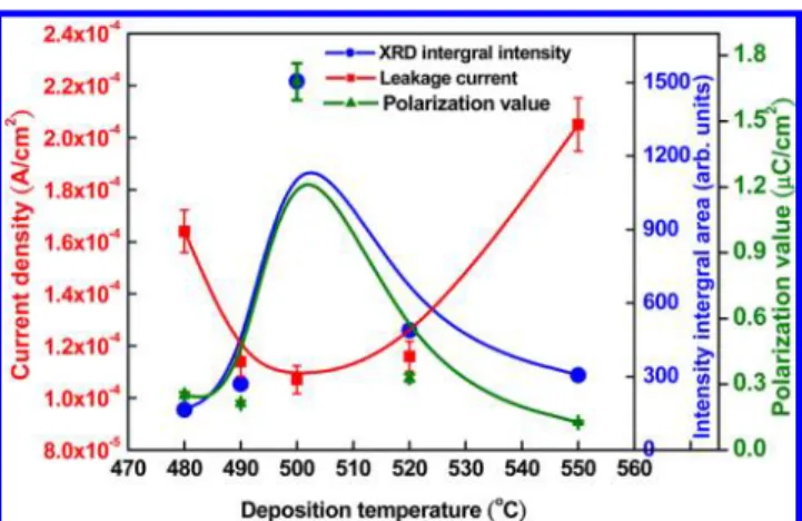
Although the leakage plays an important role in the polarization measurement, the leakage behavior affected only the saturation feature of the P−E loop because of the capacitance effect and the value of polarization. In this case, we can measure an intrinsic polarization at a condition of smaller leakage. The value of polarization was dominated by the crystalline quality, which was contributed from a large displacement of the central atom in the unit cell. In this work, the crystal structure varies greatly with the substrate temperature, as shown in Figure 10. The crystalline quality increased upon increasing growth temperature to 500 °C and decreased at greater temperature in excess of the optimal condition. The leakage current density shows a trend opposite to that of the crystalline quality, according to XRD at varied substrate temperatures.
Considering the relationship between the thickness and polarization, we collected experimental data for BFO (001) with thickness as a function of the polarization normalized with thickness shown in Figure 11. Besides ALD, all results from PLD,1,3,30 CVD,8 sol-gel,7 and RF-sputtering22,35−37 yield a statistical linear regression curve with a point of intersection of about 30 nm. A review of the literature reveals that authors also mention that it becomes difficult to measure quantitatively the ferroelectric and piezoelectric properties in a capacitor geometry below 50 nm because of a progressively larger contribution from leakage.38Our report is thus the first of a credible remanent polarization with thickness of less than 30
nm and a leakage parameter satisfactory for a FRAM application at the state of the art. Because FRAM has a cell structure similar to that of dynamic random access memory (DRAM) in a contemporary design, the growth of BFO must face the same problem as that in current DRAM devices. DRAM capacitor technology is at present more seriously challenged than that in any previous period because of the accelerated scaling of the cell size. For stacked-capacitor or vertical-transistor technology, as the dimension decreases to 20 nm, the most difficult situation faced is the insufficient space for deposition of the dielectric layers and the plate electrode because of an extremely limited area. In this case, the aspect ratio between the cap and device generally exceeds 1:50, which is a large barrier for PVD and CVD processes. ALD is a technique suitable for depositing a dielectric film and an electrode into a deep trench with improving performance of the process such as with step coverage and large throughput. As the trench narrows to 13 nm, the industry needs ALD growth for multicomponent films such as BaSrTiO3 or SrRuO3, while
maintaining both the stoichiometry and step coverage using precursors with poor reactivity (poor rate of growth). BFO currently gains much attention as a new candidate material for FRAM, but it requires a larger switching voltage, which means that the film needs to be thinner, or possibly doped, to accommodate operation at a small voltage. The minimum switching charge value Qsw(assumed to be 30μC cm−2) then yields the desired capacitor area. If this area is larger than the
Figure 9. P−E hysteresis loops of a BFO thin film for substrate temperatures in range 480−550 °C.
Figure 10.Relationship between the crystal structure, leakage current, and polarization value at varied deposition temperatures of ALD.
Figure 11.Normalized polarization as a function of thefilm thickness grown with RF-sputtering, PLD, CVD, and sol−gel and in this work with ALD.
projected size of the capacitor, a 3D capacitor should be adopted to solve this problem.39
BFO thinfilms grown with ALD show a great capability to fulfill the requirements of stoichiometry and a large rate of growth (0.087 nm cycle−1) to yield the throughput for FRAM. We reveal also that the thickness of BFO could be less than 10 nm to improve the switching voltage in a FRAM application and still retain satisfactory leakage properties. Although the polarization is not yet great enough for the desired FRAM, there are at least two ways to improve this situation: fabrication of a 3D capacitor through the advantage of ALD and growth of the BFO from the (001) to (111) direction to improve the polarization through operation of an easy axis.
■
CONCLUSIONIn this work, we clearly demonstrate a new capability to achieve a uniform fabrication of a large area and show a satisfactory performance of BFO materials to create a new application in the electroceramic field. Highly oriented BFO thin films of thickness of 10 nm were deposited on a LNO-coated Si(001) substrate with ALD. The BFO thin films show a pure single phase and acceptable crystalline quality at an optimized growth temperature of 500 °C. Both DAFS and XPS results show strong evidence of thefine stoichiometry of the BFO thin film from ALD. The HRTEM cross-sectional view shows a conformal and uniform deposition on top of the LNO buffer layer. The density of the leakage current of BFO grown with ALD shows a correct performance as well as epitaxial films, which is due to the pinhole-free and conformal growth properties of ALD to contribute a uniform BFO thinfilm on a LNO buffer layer. The excellent leakage also yields a credible remanent polarization, approximately 2Pr = 2.0 μC cm−2 obtained from a BFO thin film at 500 °C. This remanent polarization shows a strong correlation with the rate of growth; the greatest crystalline quality appeared with a growth rate near the theoretical value at an appropriate temperature. The complete mixed ternary BFO grown with ALD at an appropriate rate involved layer-by-layer growth of a O−Fe−Bi atom, reflecting an effective stoichiometry and the valence bonding in the measurement. This advantage is beneficial for IC fabrication using afilm-thickness monitor in situ, such as a quartz-crystal microbalance sensor.
■
AUTHOR INFORMATIONCorresponding Authors
*Tel.: +886(3)-5780281. Fax: +886(3)-5783813. E-mail: csku@nsrrc.org.tw.
*Tel.: +886(3)-5780281. Fax: +886(3)-5783813. E-mail: hylee@nsrrc.org.tw.
Notes
The authors declare no competingfinancial interest.
■
ACKNOWLEDGMENTSThe National Science Council of the Republic of China, Taiwan, provided support under Contracts NSC 101-2221-E-213-001-MY3 and NSC 101-2112-M-101-2221-E-213-001-MY3.
■
REFERENCES(1) Wang, J.; Neaton, J. B.; Zheng, H.; Nagarajan, V.; Ogale, S. B.; Liu, B.; Viehland, D.; Vaithyanathan, V.; Schlom, D. G.; Waghmare, U. V.; Spaldin, N. A.; Rabe, K. M.; Wuttig, M.; Ramesh, R. Science 2003, 299, 1719−1722.
(2) Ponzoni, C.; Rosa, R.; Cannio, M.; Buscaglia, V.; Finocchio, E.; Nanni, P.; Leonelli, C. J. Eur. Ceram. Soc. 2013, 33, 1325−1333.
(3) Wang, J.; Zheng, H.; Ma, Z.; Prasertchoung, S.; Wuttig, M.; Droopad, R.; Yu, J.; Eisenbeiser, K.; Ramesh, R. Appl. Phys. Lett. 2004, 85, 2574−2576.
(4) Singh, S. K.; Kim, Y. K.; Funakubo, H.; Ishiwara, H. Appl. Phys. Lett. 2006, 88, 162904-1−162904-3.
(5) Wu, J.; Wang, J.; Xiao, D.; Zhu, J. ACS Appl. Mater. Interfaces 2012, 4, 1182−1185.
(6) Liu, H. J.; Liang, C. W.; Liang, W. I.; Chen, H. J.; Yang, J. C.; Peng, C. Y.; Wang, G. F.; Chu, F. N.; Chen, Y. C.; Lee, H. Y.; Chang, L.; Lin, S. J.; Chu, Y. H. Phys. Rev. B 2012, 85, 014104-1−014104-8. (7) Wang, Y.; Lin, Y.; Nan, C. W. J. Appl. Phys. 2008, 104, 123912-1− 123912-4.
(8) Yang, S. Y.; Zavaliche, F.; Mohaddes-Ardabili, L.; Vaithyanathan, V.; Schlom, D. G.; Lee, Y. J.; Chu, Y. H.; Cruz, M. P.; Zhan, Q.; Zhao, T.; Ramesh, R. Appl. Phys. Lett. 2005, 87, 102903-1−102903-3.
(9) Eerenstein, W.; Mathur, N. D.; Scott, J. F. Nature 2006, 442, 759−765.
(10) Smolenskii, G. A.; Chupis, I. E. Sov. Phys. Usp. 1982, 25, 475− 493.
(11) Fiebig, M. J. Phys. D 2005, 38, R123−R152.
(12) Fiebig, M.; Lottermoser, Th.; Frohlich, D.; Goltsev, A. V.; Pisarev, R. V. Nature (London) 2002, 419, 818−820.
(13) Qi, X.; Dho, J.; Tomov, R.; Blamire, M. G.; MacManus-Driscoll, J. L. Appl. Phys. Lett. 2005, 86, 062903-1−062903-3.
(14) Ku, C. S.; Lee, H. Y.; Huang, J. M.; Lin, C. M. Cryst. Growth Des. 2010, 10, 1460−1463.
(15) Kwon, O. S.; Lee, S. W.; Han, J. H.; Hwang, C. S. J. Electrochem. Soc. 2007, 154, G127−G133.
(16) Hwang, G. W.; Kim, W. D.; Min, Y. S.; Cho, Y. J.; Hwang, C. S. J. Electrochem. Soc. 2006, 153, F20−F26.
(17) Lee, S. W.; Kwon, O. S.; Han, J. H.; Hwang, C. S. Appl. Phys. Lett. 2008, 92, 222903-1−222903-3.
(18) Elam, J. W.; Sechrist, Z. A.; George, S. M. Thin Solid Films 2002, 414, 43−55.
(19) Ku, C. S.; Lee, H. Y.; Huang, J. M.; Lin, C. M. Mater. Chem. Phys. 2010, 120, 236−239.
(20) Wu, C. M.; Wu, T. B. Jpn. J. Appl. Phys. 1997, 36, 1164−1168. (21) Yang, C. C.; Chen, M. S.; Hong, T. J.; Wu, C. M.; Wu, J. M.; Wu, T. B. Appl. Phys. Lett. 1995, 66, 2643−2645.
(22) Shyu, M. J.; Hong, T. J.; Wu, T. B. Jpn. J. Appl. Phys. 1995, 34, 3647−3653.
(23) Carcia, P. F.; McLean, R. S.; Reilly, M. H. Appl. Phys. Lett. 2006, 88, 123509-1−123509-3.
(24) Liu, Y. T.; Chen, S. Y.; Lee, H. Y. Thin Solid Films 2010, 518, 7412−7415.
(25) Catalan, G.; Scott, J. F. Adv. Mater. 2009, 21, 2463−2485. (26) Yun, K. Y.; Noda, M.; Okuyama, M. Appl. Phys. Lett. 2003, 83, 3981−3983.
(27) Stragier, H.; Cross, J. O.; Rehr, J. J.; Sorensen, L. B.; Bouldin, C. E.; Woicik, J. C. Phys. Rev. Lett. 1992, 69, 3064−3067.
(28) Sorensen, L. B.; Cross, J. O.; Newville, M.; Ravel, B.; Rehr, J. J.; Stragier, H.; Bouldin, C. E.; Woicik, J. C. In Resonant Anomalous X-Ray Scattering: Theory and Applications; Materlik, G., Sparks, C. J., Fischer, K., Eds.; Elsevier Science North-Holland: Amsterdam, The Nether-lands, 1994; p 389.
(29) Liu, Y. T.; Chiu, S. J.; Lee, H. Y.; Chen, S. Y. Surf. Coat. Technol. 2011, 206, 1666−1672.
(30) Shelke, V.; Harshan, V. N.; Kotru, S.; Gupta, A. J. Appl. Phys. 2009, 106, 104114-1−104114-7.
(31) Liu, H. J.; Yao, K.; Yang, P.; Du, Y. H.; He, Q.; Gu, Y. L.; Li, X. L.; Wang, S. H.; Zhou, X. T.; Wang, J. Phys. Rev. B 2010, 82, 064108-1−064108-6.
(32) Chou, A. I.; Lai, K.; Kumar, K.; Chowdhury, P.; Lee, J. C. Appl. Phys. Lett. 1997, 70, 3407−3409.
(33) Liu, Y. T.; Chen, S. Y.; Lee, H. Y. Thin Solid Films 2013, 529, 66−70.
(34) Ku, C. S.; Lee, H. Y.; Huang, J. M. Appl. Phys. Lett. 2010, 97, 181915−1-18915-3.
(35) Zheng, R. Y.; Wang, J.; Ramakrishna, S. J. Appl. Phys. 2008, 104, 034106−1-034106-6.
(36) Yeh, C. S.; Wu, J. M. Appl. Phys. Lett 2008, 93, 154101−1-154101-3.
(37) Lee, C. C.; Wu, J. M. Appl. Phys. Lett 2007, 91, 102906−1-102906-3.
(38) Chu, Y. H.; Zhao, T.; Cruz, M. P.; Zhan, Q.; Yang, P. L.; Martin, L. W.; Huijben, M.; Yang, C. H.; Zavaliche, F.; Zheng, H.; Ramesh, R. Appl. Phys. Lett 2007, 90, 252906−1-252906-3.
(39) Jose, S. Front End Processes Section; Semiconductor Industry Association: Washington, DC, 2011; pp 7−26.