Spin-orbit interaction and electron elastic scattering from impurities in quantum wells
H. C. Huang, O. Voskoboynikov, and C. P. LeeNational Chiao Tung University, 1001 Ta Hsueh Road, Hsinchu, 300, Taiwan, Republic of China 共Received 4 November 2002; revised manuscript received 24 February 2003; published 30 May 2003兲
We present a theoretical study of the spin-dependent scattering of electrons from screened impurities in III-V semiconductor quantum wells. Our calculation is based on the effective one-electronic-band Hamiltonian and the spin-orbit coupling with the Coulombic potential of the impurities. We demonstrate that the spin-orbit interaction can lead to recognizable magnitudes of spin asymmetry in the elastic-scattering cross section. Fairly large values of the Sherman function 共about 0.01兲 are obtained for repulsive and attractive impurities in quantum wells of narrow gap semiconductors.
DOI: 10.1103/PhysRevB.67.195337 PACS number共s兲: 71.70.Ej, 72.10.⫺d, 73.21.Fg
I. INTRODUCTION
A large number of studies of the electron transport in two-dimensional共2-D兲 semiconductor systems has been car-ried out over the past 40 years共see, for instance, Refs. 1–8兲. This is especially important for electronic applications. Progress in modern semiconductor technologies has allowed us to experimentally and theoretically model the various scattering mechanisms in 2-D semiconductor structures within a wide range of material parameters.4 – 8 It is com-monly accepted now that the electron mobility of a semicon-ductor 2-D heterostructure is determined by impurity scatter-ing at low temperatures and by the phonon scatterscatter-ing at high temperatures.
Recently there has been renewed interest in spin-dependent scattering and transport phenomena in semicon-ductor heterostructures because a branch of semiconsemicon-ductor electronics so called spintronics, has become a focus of in-terest 共see Refs. 9–12, and references therein兲. The extra degree of freedom provided by the electron spin opens a new field for the development of semiconductor devices. In prin-ciple, one can use the semiconductor approach to generate, control, and detect electron-spin polarization.11,13 This ap-proach has the advantage of being compatible with conven-tional semiconductor technology.
In the absence of magnetic impurities, the main source of spin-dependent scattering processes at low temperatures is spin-orbit coupling to local defects. The effect of spin-orbit interaction on spin relaxation for semiconductor 2-D systems also has been studied for a long time.14 –17Recently coherent spin transport has been demonstrated in homogeneous semi-conductors and heterostructures.19,18 Unfortunately, the theory of spin-dependent transport for semiconductor 2-D systems is still far from being complete. For this reason we recently investigated spin-dependent elastic-scattering pro-cesses in semiconductors in the presence of spin-orbit interaction.20,21 In 2-D quantum wells,20 this effect is ex-pected to be stronger than that in the bulk21 because of the localization of electronic wave functions in the conductive channel. It should be noted that the problem remains com-plicated even for the simplest models of 2-D electron motion because, in general, spin-orbit interaction should be de-scribed by a three-dimensional model.
Using the delta-doping technique, Coulomb attractive and
repulsive impurities can be precisely placed in heterostruc-tures. Using this fact one can model theoretically the scatter-ing from the impurities located inside2or outside22 the con-ductive channel. Most of the theoretical simulations of 2-D electron elastic-scattering processes from the impurities were conducted in detail in the first Born approximation.2,4 How-ever, it is well known that when perturbation theory is used, the dependence on spin in the elastic cross section appears only in the approximation that follows the first Born approximation.23–26 For this reason, one should use other approaches in calculations of the spin-dependent scattering cross section. In particular, this is the partial-wave approach,25,27 which was also used in some simulations of the spin-independent elastic-scattering cross section when the first Born approximation is not applicable.28 –30
In this paper we calculate the spin-dependent elastic-scattering cross section for electrons scattered by impurities in 2-D heterostructures of III-V semiconductors. We use the effective one-electronic-band Hamiltonian23 with Ben-Daniel-Duke boundary conditions for electronic envelope functions to calculate the spin-dependent cross section for electrons scattered from repulsive and attractive isolated im-purities with spin-orbit coupling.24 –26The impurities are lo-cated inside the quantum well. For narrow gap semiconduc-tor quantum wells 共systems with large spin-orbit coupling parameters兲 we found a large spin-related asymmetry in the cross section.
The paper is organized as follows: Section II begins with an introduction to the effective one-electronic-band 2-D Hamiltonian with impurities located inside semiconductor quantum wells. Section III gives details of the variable phase approach to spin-dependent elastic scattering in 2-D systems. The calculation results are presented in Sec. IV and conclu-sions are given in Sec. V.
II. BASIC EQUATIONS
We consider electrons in semiconductor heterostructures with charged impurities and use the approximate one-electronic-band effective Hamiltonian for the electron enve-lope wave functions
Hˆ⫽Hˆ0⫹Vˆim共r兲. 共1兲
In Eq. 共1兲 Hˆ0 is the Hamiltonian of the system without impurities,31–34 Hˆ0⫽⫺ ប2 2 “r
冋
1 m共E,r兲册
“r⫹V共r兲,where“rstands for the spatial gradient; m(E,r) is the en-ergy and position-dependent electron effective mass,
1 m共E,r兲⫽ 2 P2 3ប2
冋
2 E⫹Eg共r兲⫺V共r兲 ⫹ 1 E⫹Eg共r兲⫹⌬共r兲⫺V共r兲册
,where V(r) is the confinement potential of the well; E is the electron energy; Eg(r) and ⌬(r) stand for the
position-dependent band gap and the spin-orbit splitting in the va-lence band; P is the momentum matrix element; and Vˆim(r)
is the scattering potential of the impurity.
The impurity scattering potential consists of two parts, Vi共r兲⫽Vic共r兲⫹Viso共r兲,
where Vic(r) is the Coulomb potential of the charged
impu-rity and Viso(r) describes the spin-orbit interaction of
elec-trons with the impurity
Viso共r兲⫽⫺i␥共E,r兲“Vic共r兲•关ˆ⫻“r兴, 共2兲
where32,34 ␥共E,r兲⫽P 2 3
再
1 关E⫹Eg共r兲⫺V共r兲兴2 ⫺ 1 关E⫹Eg共r兲⫹⌬共r兲⫺V共r兲兴2冎
. 共3兲The spin-orbit interaction in the form of Eq. 共2兲 is the generalization of the well-known Rashba spin-orbit interaction,33 which comes from system inversion asymmetry.32,34In semiconductor structures with the average uniform electric field F one can consider
FÄÀ1
e “V˜p共r兲,
where e is the electron charge and V˜p(r) is the average
space-charge electric potential. When the electron with the wave vector k⬜F is moving in the field, one can readily obtain from Eq.共2兲 the well-known Rashba interaction
Vso共r兲⫽␣n•关ˆ⫻k兴,
where ␣⫽⫺e␥F and n is the unit vector parallel to the field.33
Here we consider III-V semiconductor symmetrical quan-tum wells of thickness L. In the structure we denote by z the direction perpendicular to the well interfaces, and ⫽(x,y) is the position vector parallel to the interfaces (z⫽0 is the center of the well兲. For systems with sharp discontinuity in
the conduction-band edge between the quantum well 共mate-rial 1) and the barrier region 共material 2) the potential can be presented as V共r兲⫽
再
0, ⫺L 2⭐z⭐ L 2; 共r苸1兲, V0, 兩z兩⬎ L 2; 共r苸2兲. 共4兲We assume that an isolated impurity is located at z⫽d and the unscreened Coulomb potential of the impurity is given as
Vic0共r兲⫽ Ze 2 s关2⫹共z⫺d兲2兴1/2
, 共5兲
where s is the relative permittivity of the system and Z is
the charge of the impurity. For most III-V quantum wells we can neglect the image potential and use for simplicity s
⫽(1⫹2)/2 (1 and2 are the dielectric constants of ma-terials 1 and 2, correspondingly兲.
Following Refs. 1, 2, and 31 we present the solution of the confinement problem with the Hamiltonian Hˆ0 as
⌿n,s共,z兲⫽s共兲n共z兲,
where n labels the eigenenergies in the normal direction (En), and s⫽⫾1 is the quantum number related to the spin
polarization along the z direction.
As is shown in Ref. 32, due to the reflection symmetry of the well in the z direction共there are no built-in electric fields兲 the Rahsba spin splitting in the electron spectrum does not occur and one can use the conventional Ben-Daniel-Duke boundary conditions31 for the wave functionn(z),
n共z兲, 1 m共E,z兲 d dzn共z兲 continuous at z⫽⫾L 2. 共6兲
Considering for simplification only the first subband as being populated we describe only intrasubband elastic-scattering processes. First we obtain the ground state 共the first subband with n⫽1). The wave function of this ground state has the well-known form
1共z兲⫽
再
A cosz, 兩z兩⭐L 2; B exp共⫺z兲, 兩z兩⬎L 2; 共7兲 where ⫽冑
2m1共E兲E1/ប, ⫽冑
2m2共E兲共V0⫺E1兲/ប,and E⫽E⫹E1consists of the energies of the and z direc-tions of motion, correspondingly. From the Ben-Daniel-Duke boundary conditions共6兲 we obtain the spinless transcenden-tal equation
tan关共E,E1兲L/2兴⫽
m1共E兲共E,E1兲 m2共E兲共E,E1兲
. 共8兲
Equation共8兲 gives us the eigenenergy in the z direction in an implicit form.
The wave function 共7兲 共after proper normalization兲, we substitute into the three-dimensional Schro¨dinger equation with the Hamiltonian 共1兲 and integrate out the z coordinate by taking the average,
Hˆ⫽
冕
⫺⬁ ⫹⬁
dz1*共z兲Hˆ1共z兲.
After the averaging and introducing the screening of the im-purity at low temperatures by means of Refs. 1 and 23 the quasi-2-D Schro¨dinger equation in the polar coordinates Ä(,) is given by
冋
1 冉
冊
⫺ 1 2 2 2⫺V˜共兲⫹isW˜共兲 ⫹k2册
s共兲⫽0, 共9兲 where V ˜共兲⫽2Z aB* m˜共E兲 m1共0兲冕
0 ⬁ dq 共q兲J0共q兲冕
⫺⬁ ⫹⬁ dz兩1共z兲兩2e⫺q兩z⫺d兩 is the statically screened Coulomb potential in the quantum well plane, W˜共兲⫽⫺ 2Z aB* m˜共E兲 m1共0兲冕
0 ⬁qdq 共q兲J1共q兲 ⫻冋
␣1共E兲冕
z⭐兩L/2兩 dz兩1共z兲兩2e⫺q兩z⫺d兩 ⫹␣2共E兲冕
z⭓兩L/2兩 dz兩1共z兲兩2e⫺q兩z⫺d兩册
is the screened spin-orbit interaction, aB*⫽sប2/e2m1(0) is the effective Bohr radius in the well,k2⫽2m ˜共E兲E ប2 , 1 m˜共E兲⫽ 1 m1共E兲
冕
z⭐兩L/2兩 dz兩1共z兲兩2 ⫹ 1 m2共E兲冕
z⭓兩L/2兩 dz兩1共z兲兩2, Jn(x) is the Bessel function,共q兲⫽1⫹qf
q is the 2-D electronic dielectric function,
q f⫽ e2m 1共EF兲 2ប2s
再
1⫹ d dEln关m1共E兲兴冏
EF冎
is the 2-D Thomas-Fermi screening constant in the degener-ated electronic system, and EF is the Fermi energy of the
system.35The Fermi wave vector kF(EF) must be defined by
means of the solution of the following equation:
EF⫽ ប2k F 2 2m1共EF兲 .
III. TWO-DIMENSIONAL ELASTIC SCATTERING AND SHERMAN FUNCTION
Due to the radial symmetry of the potentials V˜c() and
W˜ () in Eq.共9兲 the method of partial waves is convenient for our consideration. One can separate variables in the ex-pression for the wave function as the following:23–25
s共兲⫽
兺
l⫽⫺⬁ l⫽⫹⬁Rls共兲eils,
where l is the orbital momentum number and s is a spin function upon which the Pauli matrix vector operates,
⫹1⫽
冉
10
冊
, ⫺1⫽
冉
01
冊
.The Schro¨dinger equation for the radial wave function be-comes of the following form:
冋
1 d d冉
d d冊
⫺ l2 2⫺V˜共兲⫺slW˜共兲⫹k 2册
R l s共兲⫽0.At a large distance from the scattering center the asymtotic value of the radial function is given by
Rls共兲→Als关cos␦lsJl共k兲⫺sin␦lsNl共k兲兴; →⬁, where ␦l
s
is the spin-dependent scattering phase shift24 –27 and Nl is the Neumann function.
In the variable phase approach27,36 the phase function ␦l
s
() at the point determines the phase shift produced by the part of the potential contained within the cycle of a radius . The scattering phase shift for the total potential is equal to the asymptotic value
␦l s⫽ lim
→⬁␦l s共
兲.
The phase function␦ls() satisfies the following differential equation:27,36
d␦l s共兲 d ⫽⫺ 2关V˜共兲⫹slW˜共兲兴关cos␦l s共兲J l共k兲 ⫺sin␦l s共兲N l共k兲兴2 共10兲
with the boundary condition ␦l
s共0兲⫽0. 共11兲
The complex 2-D scattering amplitude can be expressed as20,24,25
Fs共兲⫽关 f 共兲⫹zg共兲兴s, 共12兲
where fs() and g() describe scattering without and with electron-spin reorientation, and they are determined by the expressions f共兲⫽
兺
l⫽0 ⬁ flcos共l兲, 共13兲 g共兲⫽兺
l⭓1 ⬁ glsin共l兲, 共14兲 where fl⫽冑
1 2k再
exp共2i␦0兲⫺1; l⫽0;exp共i2␦l⫹兲⫹exp共i2␦l⫺兲⫺2; l⭓1; gl⫽i
冑
1
2k 关exp共i2␦l⫹兲⫺exp共i2␦l⫺兲兴,
where is the scattering angle between initial (ki) and final
(kf) wave vectors.
The Mott scattering24cross section for electrons spin po-larized parallel to the z axis can be expressed in terms of the incident electron-beam spin polarization Pialong the z
direc-tion as the following:
共兲⫽I共兲关1⫹S共兲Pi兴, 共15兲
where I() is the differential cross section for unpolarized incident electrons,
I共兲⫽兩 f 共兲兩2⫹兩g共兲兩2, 共16兲 and
S共兲⫽f*共兲g共兲⫹ f 共兲g*共兲
兩 f共兲兩2⫹兩g共兲兩2 共17兲 is the Sherman function for 2-D electrons. The Sherman function is an important characteristic of the spin-dependent scattering 共see Refs. 37 and 38, and references therein兲. It presents the left-right asymmetry in the scattering cross sec-tion for initially polarized electron beams and the average polarization of unpolarized electrons after the scattering. This characteristic is important in the evaluations of the anomalous Hall effect in different materials and structures.
For degenerated electronic systems, for instance, the Hall angle is proportional to the Sherman function at the Fermi energy shell.26,39– 41
IV. CALCULATION RESULTS
To present the realistic estimation of the effect of the spin-orbit coupling on the electron elastic cross section we choose two types of symmetrical quantum well structures: type I is Al0.48In0.52As/In0.53Ga0.47As/Al0.48In0.52As 共where Eg1⫽0.813 eV, Eg2⫽1.508 eV, ⌬1⫽0.361 eV, ⌬2 ⫽0.332 eV, m1(0)⫽0.041m0, m2(0)⫽0.075m0, 1⫽14, 2⫽12.5, V0⫽0.504 eV,41m0is the free-electron mass兲 and type II is CdTe/InSb/CdTe 关where Eg1⫽0.24 eV, Eg2 ⫽1.59 eV, ⌬1⫽0.81 eV, ⌬2⫽0.8 eV, m1(0)⫽0.015m0, m2(0)⫽0.08m0, 1⫽16.8, 2⫽10.2, V0⫽0.55 eV 共Refs. 42 and 43兲兴. While type I presents quantum well structures with well-developed growth technology, type II demonstrates
FIG. 1. The scattering cross section for the screened impurities in the type-I structure (L⫽20 nm): 共a兲 repulsive (Z⫽⫹1) impu-rity; 共b兲 attractive (Z⫽⫺1) impurity; 共c兲 the ratio between the complete numerical result (exact) and the first Born approximation (Born) for the repulsive impurity when kaB*⫽1.8 (E⫽0.01 eV).
the largest spin-coupling effects. In all calculations we assure the validity of the one-subband scattering model,when the intersubband gap is larger than the energy of the-direction motion: E⬍E2⫺E1. This allows us to consider scattering of electrons with the following wave vectors: for type-I structures with L⭐30 nm, k⭐kFI⫽2.5(aB*)⫺1 共the electron concentration ns⫽3.5⫻1011 cm⫺2); for type-II structures with L⭐30 nm, k⭐kFII⫽6.6(aB*)⫺1 (ns⫽3⫻1011 cm⫺2).
Notice that aB*is taken to be different according to the defi-nitions for the different types of the systems.
The phase shifts were obtained by the numerical solution of Eq. 共10兲 with the initial condition of Eq. 共11兲 and then used in Eqs. 共12兲–共17兲 to calculate the elastic-scattering cross section. From our calculation experience the conver-gence criteria on the cross section共the maximum net error is less than 10⫺4) can be reached by taking the necessary num-ber兩l兩⭐70 of the partial waves included Eqs. 共13兲 and 共14兲. Figure 1 shows energy and angle dependencies of the elastic-scattering cross section for 2-D electrons scattered from at-tractive (Z⫽⫹1) and repulsive (Z⫽⫺1) impurities located in the center of the type-I structure. The cross sections dem-onstrate the well-known logarithmic divergence at zero en-ergy (E→0) for both types of impurities 共repulsive and attractive兲.28 In Fig. 1共c兲 we compare our results with the cross section obtained within the first Born approximation27,28when fl⬇⫺
冑
2k冕
0 ⬁ Jl2共k兲V˜共兲d⫻再
1, l⫽0; 2, l⭓1; 共18兲 gl⬇il冑
2k冕
0 ⬁ Jl2共k兲W˜共兲d⫻再
1, l⫽0; 2, l⭓1. 共19兲 It is known1,44that the first Born approximation is valid for 2-D elastic scattering whenkaB*Ⰷ1.
It is worth noting, that the numerically calculated cross sec-tion for the 2-D screened Coulomb potential is different from that obtained in the first Born approximation near the edge of the approximation validity (kaB*⫽1.8). In addition, it can be
seen from Eqs.共18兲 and 共19兲 that in the first Born approxi-mation all spin-polarization effects in the elastic cross sec-tion vanish:23,24,26
S共兲⬃ f*共兲g共兲⫹ f 共兲g*共兲⫽0.
Thus, the Sherman function should be calculated only by going beyond the first Born approximation and taking into consideration the higher partial waves (兩l兩⬎0). The com-plete numerical solution allows us to do that.
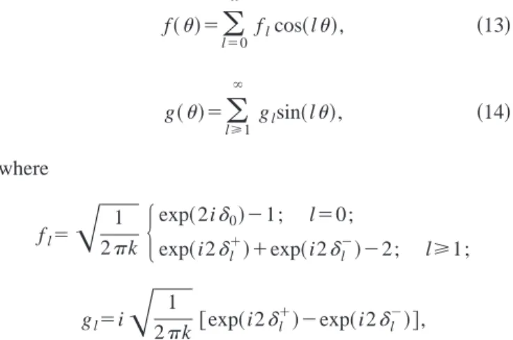
Figure 2 shows the Sherman functions for the type-I structure, when the repulsive 关Fig. 1共a兲兴 and attractive 关Fig. 1共b兲兴 impurities are located in the center of the well with the width L⫽20 nm. We first note that, in the energy range con-sidered, the effect is slightly larger for the repulsive scatter-ing center. Since S() is closely connected to the cross
sec-FIG. 2. The Sherman function for the type-I structure (L
⫽20 nm): 共a兲 repulsive impurity; 共b兲 attractive impurity.
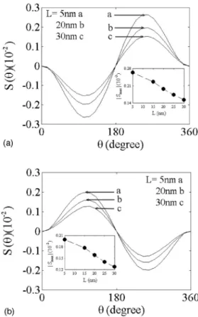
FIG. 3. The Sherman function for the type-I structures with different well widths (E⫽0.02 eV): 共a兲 repulsive impurity; 共b兲 attractive impurity. Insets: the dependencies of the Sherman func-tion amplitude on the well width.
tion curves, the high values of the Sherman function occur where the cross-section is small and vice versa. The change of the impurity sign leads to inversion in the three-dimensional plots. This is a direct and clear consequence of sign altering in the potentials V˜ () and W˜ () 关see Eq. 共10兲兴. It can be seen that with suitable electron energies and the large scattering angles one can reach polarizations of more than 0.1%.
In our simulation we found a decrease in the polarization effect when well width increases. The dependence of the Sherman function on the well width L for the type-I structure is presented in Figs. 3共a兲 and 3共b兲 共the impurity is located in the center of the well: d⫽0). This decrease is obviously connected to the form of the averaged effective potentials V
˜ () and W˜ (). The various potentials for different well widths are shown in Fig. 4. The curves represent the absolute value of the potentials关for the repulsive center V˜() is posi-tive and W˜ () is negative; for the attractive center V˜ () is negative and W˜ () is positive兴 and demonstrate the influence of the 2-D confinement and screening on the elastic scatter-ing processes in quantum wells.2,3,28 The figure shows that the spin-orbit coupling potential becomes stronger near the impurity site when the well width decreases. Electrons that are scattered at large angles 共where the polarization effects are expected to be higher兲 pass through the relatively strong fields at fairly small distances from the impurity site. This
causes the stronger polarization effects for the relatively nar-row wells共as is shown in the insets of the Fig. 3兲. This result suggests the possibility of controlling Sherman function by means of the well size.
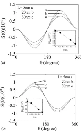
The spin-orbit interaction is known to be larger in small gap semiconductors. Based on this fact, we show in Fig. 5, as an example, the calculation results for the type-II structures. The asymmetry effect in the scattering cross section for those structures can reach about 1% for electrons with moderate energy, when the impurity is located in the center of the well. The insets show the dependencies of the amplitude of the Sherman function on the position of the impurity in the wells. Obviously, the magnitude of the Sherman function de-creases when d inde-creases. But the effect remains valuable even for the impurities located at the edge of the well (d ⫽L/2).
In addition, we notice that the spin-dependent asymmetry for the elastic-scattering cross section for the impurities lo-cated in the wells 共2-D systems兲 is significantly larger than calculated for 3-D spin-dependent elastic scattering from im-purities in the bulk. To demonstrate the difference we present in Table I our results for the type-II structure and results obtained in Ref. 26 and 39, when all parameters of the sys-tems are chosen the same 共the systems differ only in the dimensionality兲. In the table, ␦0 is the phase shift for l⫽0 and ␦1s pin is the correction to the phase shift of the partial wave with l⫽1 when the spin-orbit coupling is included.
FIG. 4. The dependencies of the effective averaged potentials on the well width for the type-I structures:共a兲 spinless part V˜(), 共b兲 spin-orbit coupling part W˜ ().
FIG. 5. The Sherman function for the type-II structures with different well widths (E⫽0.04 eV): 共a兲 repulsive impurity; 共b兲 attractive impurity. Insets: the dependencies of the Sherman func-tion amplitude on the impurity locafunc-tion in the well.
This result suggests that the spin-orbit coupling with the charged impurities in 2-D systems can provide sufficiently larger spin-dependent effects than those in the bulk.
V. CONCLUSIONS
We have presented a theoretical study of the elastic spin-dependent scattering of 2-D electrons from the screened Coulomb centers located in quantum wells. The one-electronic-band effective Hamiltonian and spin-orbit cou-pling potential of the impurities allow us to calculate the left-right asymmetry in the electron elastic-scattering cross section. We have found a large spin-dependent asymmetry in the cross section for electrons scattered from impurities in AlInAs/InGaAsAs/AlInAs and CdTe/InSb/CdTe symmetrical quantum wells.
For the CdTe/InSb/CdTe quantum well we found that the spin-orbit coupling in the two-dimensional systems leads to larger spin-dependent asymmetry in the scattering cross sec-tion than that in the bulk. The calculated amplitude of the Sherman function for this structure is more than 0.01. This could be detected in the measurements of the Hall effect at low temperatures26,39,40,45and this is potentially useful in in-tegrated electron-spin polarization devices based on semi-conductor heterostructures. It also can be used as a tool to determine spin-coupling parameters in III-V narrow gap semiconductor heterostructures.
Finally, we would like to point out that the described ef-fect is a clear analog of the well-known efef-fect of spin-dependent scattering in magnetic materials共see Ref. 37兲, but it can also be realized in nonmagnetic semiconductor struc-tures. Our model can be used as the starting point for more detailed calculations. Experimental investigations need to be conducted to verify our theory predictions.
ACKNOWLEDGMENTS
This work was supported by the National Science Council of the Republic of China under Contract Nos. NSC-90-2215-E-009-022 and NSC-91-2119-M-009-003.
1F. Stern and W. E. Howard, Phys. Rev. 163, 816共1967兲. 2T. Ando, A. B. Fowler, and F. Stern, Rev. Mod. Phys. 54, 437
共1982兲.
3C. Weisbuch and B. Vinter, Quantum Semiconductor Structures,
Fundamental and Applications共Academic, New York, 1991兲.
4W. Walukiewicz, H. E. Ruda, J. Lagowski, and H. C. Gatos, Phys. Rev. B 30, 4571共1984兲.
5L. Pfeiffer, K. W. West, H. L. Stormer, and K. W. Baldwin, Appl. Phys. Lett. 33, 665共1978兲.
6M. Kudo, T. Mishima, T. Tanitomo, and M. Washima, Jpn. J. Appl. Phys., Part 1 33, 971共1994兲.
7M. L. Ke, D. Westwood, R. H. Williams, and M. J. Godfrey, Phys. Rev. B 51, 5038共1995兲.
8
J. Dickman, Appl. Phys. Lett. 60, 88共1992兲. 9G. A. Prinz, Science 282, 1660共1998兲.
10J. Fabian and S. Das Sarma, J. Vac. Sci. Technol. B 17, 1708
共1999兲.
11H. Ohno, J. Vac. Sci. Technol. B 18, 2039共2000兲.
12P. R. Hammar and M. Johnson, Phys. Rev. B 61, 7207共2000兲. 13C. M. Hu, J. Nitta, A. Jensen, J. B. Hansen, H. Takayanagi, T.
Matsuyama, D. Heitman, and U. Merkt, J. Appl. Phys. 97, 7251
共2002兲.
14M. I. D’yakonov and V. Yu. Kachorovskii, Fiz. Tekh. Polupro-vodn. 20, 178共1986兲 关Sov. Phys. Semicond. 20, 100 共1986兲兴. 15Y. A. Bychkov and E. I. Rashba, Pis’ma Zh. E´ ksp. Teor. Fiz. 39,
66共1984兲 关JETP Lett. 39, 78 共1984兲兴.
16V. M. Edelstein, Physica B 284–288, 1217共2000兲. 17T. P. Pareek and P. Bruno, Pramana, J. Phys. 57, 1共2002兲. 18J. M. Kikkawa and D. D. Awschalom, Phys. Rev. Lett. 80, 4313
共1998兲.
19I. Malajovich, J. M. Kikkawa, D. D. Awschalom, J. J. Berry, and N. Samarth, Phys. Rev. Lett. 84, 1015共2000兲.
20O. Voskoboynikov, H. C. Huang, C. P. Lee, and O. Tretyak, Physica E共Amsterdam兲 12, 252 共2002兲.
21Edward Chen, O. Voskoboynikov, and C. P. Lee, Solid State Commun. 125, 381共2003兲.
22W. T. Masselink, Phys. Rev. Lett. 66, 1513共1991兲.
23A. S. Davydov, Quantum Mechanics共Pergamon, London, 1965兲. 24N. F. Mott and H. S. Massey, The Theory of Atomic Collisions,
3rd ed.共Oxford University, London, 1987兲.
25C. J. Joachain, Quantum Collision Theory共North-Holland, Am-sterdam, 1979兲.
26
V. N. Abakumov and I. N. Yassievich, Zh. E´ ksp. Teor. Fiz. 61, 2571共1972兲 关Sov. Phys. JETP 34, 1375 共1972兲兴.
27F. Cologero, Variable Phase Approach to Potential Scattering
共Academic, New York, 1967兲.
28P. G. Averbuch, J. Phys. A 19, 2325共1986兲.
29I. A. Larkin, Fiz. Tekh. Poluprovodn. 22, 2008共1988兲 关Sov. Phys. Semicond. 22, 1271共1988兲.
30M. E. Portnoi and I. Galbreith, Solid State Commun. 103, 325
共1997兲.
31G. Bastard, Wave Mechanics Applied to Semiconductor
Hetero-structures共Les Editions de Physique, Les Ulis, 1990兲.
32E. A. de Andrada e Silva, G. C. La Rocca, and F. Bassani, Phys. Rev. B 55, 16 293共1997兲.
33
Yu. A. Bychkov and E. I. Rashba, J. Phys. C 17, 6039共1984兲. 34Th. Scha¨pers, G. Engels, J. Lange, Th. Klocke, M. Hollfelder, and
H. Lu¨th, J. Appl. Phys. 83, 4324共1998兲.
35D. K. Ferry and S. M. Goodnick, Transport in Nanostructures
TABLE I. The ratio ⫽␦1
s pin
/␦0 for InSb structures (L⫽5 nm).
Impurity type for 3-D systema for 2-D system
Z⫽⫺1 3.7⫻10⫺5 2.8⫻10⫺2
Z⫽⫹1 2.3⫻10⫺6 2.7⫻10⫺2
共Cambrige University, Cambridge, England, 1997兲.
36A.G. Sitenko, Scattering Theory共Springer-Verlag, Berlin, 1990兲. 37J. Kessler, Polarized Electrons共Springer-Verlag, Berlin, 1985兲. 38
T. J. Gay and F. B. Dunning, Rev. Sci. Instrum. 63, 1635共1992兲. 39J. N. Chazalviel, Phys. Rev. B 11, 3918共1975兲.
40G. Bergmann, Phys. Rev. B 63, 193101共2001兲.
41S. L. Chuang, Physics of Optoelectronic Devices 共Wiley-Interscience, New York, 1995兲.
42E. T. Yu, J. O. McCaldin, and T. C. McGill, Solid State Phys. 46, 2共1992兲.
43Handbook Series on Semiconductor Parameters, edited by M. Levinshtein, S. Rumyantsev, and M. Shur共World Scientific, Sin-gapore, 1999兲.
44G. Barton, Am. J. Phys. 51, 420共1983兲.