This article was downloaded by: [National Chiao Tung University 國立交通大 學]
On: 27 April 2014, At: 23:52 Publisher: Taylor & Francis
Informa Ltd Registered in England and Wales Registered Number: 1072954 Registered office: Mortimer House, 37-41 Mortimer Street, London W1T 3JH, UK
Ferroelectrics
Publication details, including instructions for authors and subscription information: http://www.tandfonline.com/loi/gfer20
Sol-Gel derived (Ba
0.5Sr
0.5)TiO
3thin films and their electrical
and dielectric properties
M. Nayak a , S. Y. Lee a & Tseung-Yuen Tseng a a
Department of Electronics Engineering , Institute of Electronics National Chiao-Tung University , 1001 Ta Hsueh Rd, Hsinchu, 300, Taiwan, R.O.C.
Published online: 26 Oct 2011.
To cite this article: M. Nayak , S. Y. Lee & Tseung-Yuen Tseng (2001) Sol-Gel derived (Ba0.5Sr0.5)TiO3 thin films and their electrical and dielectric properties, Ferroelectrics, 259:1, 239-249, DOI: 10.1080/00150190108008744
To link to this article: http://dx.doi.org/10.1080/00150190108008744
PLEASE SCROLL DOWN FOR ARTICLE
Taylor & Francis makes every effort to ensure the accuracy of all the information (the “Content”) contained in the publications on our platform. However, Taylor & Francis, our agents, and our licensors make no
representations or warranties whatsoever as to the accuracy, completeness, or suitability for any purpose of the Content. Any opinions and views
expressed in this publication are the opinions and views of the authors, and are not the views of or endorsed by Taylor & Francis. The accuracy of the Content should not be relied upon and should be independently verified with primary sources of information. Taylor and Francis shall not be liable for any losses, actions, claims, proceedings, demands, costs, expenses, damages, and other liabilities whatsoever or howsoever caused arising directly or indirectly in connection with, in relation to or arising out of the use of the Content.
expressly forbidden. Terms & Conditions of access and use can be found at http://www.tandfonline.com/page/terms-and-conditions
Sol-Gel Derived (Ba0.5Sr0.5)Ti03 Thin Films and their
Electrical and Dielectric Properties
M.NAYAK, S.Y.LEE and TSEUNG-YLJEN TSENG
Department of Electronics Engineering and Institute of Electronics National Chiao-Tung University,
IOOI
Ta Hsueh RdHsinchu-300, Taiwan, R.O. C.
(Received in fino/ form Augirsr 3. 2001)
Barium strontium titanate thin films with composition (Ba0.5Sro.s)Ti03 were prepared by a sol-gel method using hydroxide-alkoxide precursors. Reasonably well-crystallized film was obtained at a temperature as low as 5OO0C. The leakage current characteristics and dielectric constant of the films varied with the annealing temperature due to the change in microstructure. The electrical and dielectric properties of the films showed strong dependence on the precursor solution concentration, Dielectric response of the films prepared from dilute solution is superior to that prepared from the concentrated solution. The change in electrical and dielectric ,characteristics of the films has been correlated to their microstructure, which revealed that the concentration change affected the grain size distribution, film porosity and morphology.
Key words:
dielectric constant
sol-gel; thin film; barium strontium titanate (BST);
INTRODUCTION
Thin films of high dielectric constant materials such as barium strontium titanate (BST) have been widely investigated for their feasibility in thin fdm integrated storage capacitors in giga bit dynamic
739
random access memory (DRAM). This is mainly due to their high dielectric constant, low dielectric loss, low leakage current, low temperature coefficient of dielectric constant and the composition dependent Curie temperature [l]. In addition to the DRAM application, BST thin films have variety of other applications which are currently being studied such as hydrogen gas sensors [2], pyroelectric sensors [3,4], as a dielectric layer in electroluminescent display devices [ 5 ] and the new class of frequency tunable microwave devices, which include phase shifters, tunable filters, steerable antennas, varacters, fiequency triplers, etc. [ 6 ] . BST thin films have been prepared by variety of methods such as sputtering [7,8], laser ablation [9], chemical vapour deposition [ 101, metal-organic decomposition [ 111 chemical solution deposition [ 121, and sol-gel method [13]. Among these methods, sol-gel processing offers some advantages over the other methods in terms of compositional homogeneity, ability to coat large area and complex shaped substrates, purity because of the liquid form of precursors which can be easily purified by distillation, cost effective and simple.
In the present study we investigated the electrical and dielectric properties of the Bao.sSro.sTi03 thin films prepared by a sol-gel method using hydroxide-alkoxide precursors. Burhanuddin et. al [ 121 prepared Bao.sSro.sTi03 using Ba- and Sr-hydroxide as the source of Ba- and Sr and studied the I-V characteristics of MIS-type device. However, detailed investigation of electrical and dielectric properties has not been carried out.
EXPERIMENTAL DETAILS
The Ba&3r0.5TiO3 thin films were prepared following a procedure similar to Burhanuddin's method [ 121. Multicomponent BST precursor solution was prepared by using high purity Ba(OH)2.8H20, Sr(OH)2.8HzO and titanium (1% isopropoxide (Ti(OC3HT)d) as the precursors and 2-methoxy ethanol as the solvent. The required amounts of these precursors were separately mixed in 2-methoxy ethanol and refluxed at 12OOC for 3-4h. These three solutions after cooling to room temperature were then mixed and refluxed at 12OOC for 3h to form a homogeneous mixture of BST-precursor. Thin films were prepared by spin coating solutions of different concentration
SOL-GEL DERIVED BST THIN FlLMS 24 I
(0.28M, 0.15M, 0.08M) on to Pt/Ti/SiOz/Si substrates followed by solvent evaporation at 140°C and then pyrolysed at 500°C. After depositing the films of appropriate thickness by repeating the spin coating-solvent evaporation-pyrolysis steps, the films were finally annealed at different temperatures in the range 500-800°C. Phase formation characteristics were studied using X-ray diffraction (XRD, Shimadm XD-5). Film thickness and microstructure were characterized by scanning electron microscopy (SEM, Hitachi S4700). The capacitance-voltage
(C-V)
characteristics were measured by using Hewlett-Packard (Hp) HP4194A impedance/gain phase analyser at 100kHz
as a hnction of sweeping voltage from positive to negative voltage dc-bias. The current-voltage (I-V) measurements were performed by using HP4156A under both negative and positive voltage sweeps.RESULTS
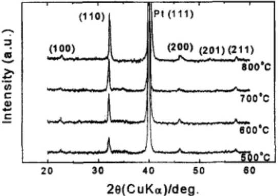
AND DISCUSSIONFigure 1 shows the
XRD
patterns of the films post annealed at different temperatures, which indicates formation of a reasonably well- crystallized film at a temperature as low as 500°C. There is no preferential orientation observed in the XRD pattern and the films deposited are polycrystalline in nature. The intensity of (110) peak increased on annealing at higher temperatures indicating theoOc
20 30 4 0 5 0 6 0
&+
1
28( C uKa)ldeg.
FIGURE 1 XRD patterns of the Bao.&o.rTi03 thin film annealed at different temperatures.
improvement in the crystallinity. The average grain size of the films determined using Scherrer’s equation [ 141 indicates that increase in annealing temperature resulted in grain growth. The 500°C annealed sample showed an average grain size of -20 nm increased to 32 nm on annealing above 600°C.
SEM surface micrographs of the BST thin films annealed at different temperatures are presented in Figure 2. The micrographs of the films annealed at 500 and 600°C show crack fiee, uniform and smooth microstructure composed of ultrafine grains. The 6OOOC annealed film shows slightly larger grain size than the 5OO0C annealed film and also shows locally crystallized sites, which act as the nucleation-sites and grow as the temperature of annealing increased. The reason for these preferential nucleation centers might be originating from the surface roughness on the bottom electrode caused by the Ti-diffusion at this temperature [15,16]. The 700°C annealed film shows uniform spherical grains of 40-70 nm size along with nanosized porosity formed because of the growth of ultra fine grains formed at low temperatures and also due to the escape of carbonatious
FIGURE 2 SEM micrographs of the BST thin film annealed at different temperatures (a) 500°C (b) 6OO0C (c) 700°C and (d) 800°C for 2h in air.
SOL-GEL DERIVED BST THIN FILMS 743
decomposition products embedded in the film. Annealing of the sample at 800OC further increased the grain size and the majority of the pores are eliminated by sintering of the film at this temperature as indicated by the micrograph. The grain size distribution in the 800OC annealed film is large ranging from 25 to 100 nm. This type of wider grain size distribution reduces the film porosity. Results indicate that, grain size increased with the annealing temperature because of the grain growth occurring at those temperatures.
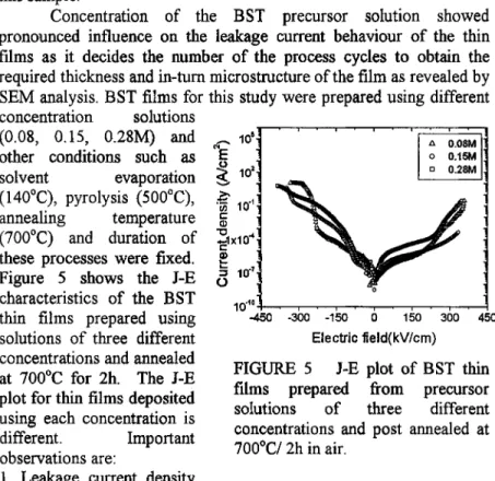
Figure 3 shows the SEM surface images of the BST thin films of thickness around 320 nm prepared using three different concentration precursor solutions and annealed at 7OO0C, which indicates different microstructure.
Film prepared from 0.08M FIGURE 3 SEM micrographs solution shows more irregular of the BST thin films prepared shaped grains of size in the range from (a) 0.08M, (b) 0.15M and 40-70 nm, whereas the films (c) 0.28M precursor solutions prepared from 0.15M solution and annealed at 700°C/2h in air. show spherical grains in the same
size range and that of 0.28 M solution shows more agglomerated irregular shaped grains. The remarkable difference between these films is in the grain morphology and the porosity. Film prepared from 0.08 M precursor solution is less porous and the films prepared from 0.15 and 0.28M solution are highly porous. These results indicate that as the solution concentration increases the porosity in the film also increases. The lower porosity in the film deposited using dilute solution is due to the fact that, each thin layer is pyrolysed individually
and hence will be thermally cycled more times than film prepared from the concentrated solution which requires less number of layers to attain same thickness. The individual layers are thicker than the film prepared from dilute solution and incorporates more carbonatious decomposition products in the film. On annealing at 700°C these embedded impurities burn-off leaving behind pores in the film and in the process changes the microstructure.
The leakage current density vs. electric field (J-
E) plot of the BST thin films annealed at different temperatures (Fig. 4) shows variation. Film annealed at 500°C shows larger leakage current than those annealed at higher temperatures. The lowest leaks e current (lod
A/cm in the electric field range <lOOkV/cm) is observed for the film annealed at 600 and 700°C. Leakage current density of the film annealed at 800°C is higher than those
ci
10' N "s
3
g
10" ~ 1 x 1 0 "5
10' c Q c 8 0 -450 -300 -150 0 150 300 450 Electric field (kVlcrn)FIGURE
4J-E
plot of BSTthin
films post annealed at different temperatures for 2h in air.annealed at 600 and 700"C, but is lower
than
that of 500°C annealed film. The J-E characteristics of all the samples show three different regions indicating the three different types of conduction mechanisms at low, intermediate and high field regions. At lower voltage the film shows ohmic behaviour and deviates at intermediate and higher fields. The turn-on electric field from ohmic to non-ohmic region decreased as the annealing temperature increased. The turn-on electric field for the sample annealed at 500 and 600°C is around 300kV/cm and that of film annealed at 700 and 8OO0C is around 2OOkV/cm and 15OkV/cm respectively. The leakage current of the samples prepared by the present method is comparable to that reported in literature for the thin films of Ba.7Sr0.3Ti03 prepared using acetate precursors and spin coated on Pt/Ti/SiOz/Si substrate [13]. The 600°C annealed sample in the present study at 75kV/cm showed leakage current of 8x1 07A/cm2,SOL-GEL DERIVED BST THIN FILMS 2445
in comparison to the reported value for the film prepared from acetate precursors ~ . ~ x I o - ~ A / c ~ ~ [ ~ ~ I .
The leakage current characteristics of the thin film capacitor depends upon several factors such as the top and bottom electrode interface, surface roughness, formation of interfacial low impedance layer or presence of any impurity second phase in the dielectric film which provides an easy path for electrons can dramatically increase the leakage current. High leakage current observed in the case of 500°C annealed samples is due to the presence of embedded pyrolysed decomposition products in the film which provide low impedance path. The decrease in the leakage current as the annealing temperature increased is because of the burn-off of the embedded decomposition products. Increase in leakage current for the film annealed at 800°C is due to the increase in the grain size, as observed by SEM analysis, which contributes to surface roughness. The grain size effect on the leakage current characteristics is more prominently reflected in the turn-on voltage. It is reported that in BST film turn-on voltage increases as the grain size decreases [7]. The films with smaller grain size, similar to the films annealed at 500 and 600°C is expected to show higher turn-on voltage and as the grain size increases the turn-on voltage is also expected to shift to the lower voltages. The smaller grain size produces more grain boundaries. Also, grain boundaries are more resistive than the bulk. Film with lower grain size will contain more grain boundaries than that with a higher grain size. Hence, it requires higher field to achieve turn-on from ohmic to non-ohmic region in the case of film with lower grain size [7].
The leakage current characteristics are distinctly different in the positive and negative voltage region. Figure 4 shows that J-E characteristics are not symmetric as expected for MIM-type of structure. In the negative voltage region the film annealed at 800°C shows maximum leakage current and the minimum is for the 500°C annealed film. The turn-on voltage for the 600, 700 and 800°C annealed samples is as low as 5OkV/cm and that of 500°C annealed sample is 250kV/cm.
The asymmetry in positive and negative voltage part of the J-E characteristics is normally brought-in due to the difference in the top and bottom electrode work functions, the difference in two interfaces and also implies that the leakage current is electrode-limited [8]. In the present case, the reason for the asymmetry in the J-E characteristics is
due to the difference in the top and bottom electrode interfaces. The difference in interface is brought about by Ti migration to the surface of the bottom Pt-electrode through grain boundaries and formation of an additional interfacial layer [ 15,161. The formation of the interfacial layer also depends upon annealing temperature.
As
the annealing temperature increases the difhsion rate increases and more and more Ti migrates to the surface of Pt through grain boundaries and reacts with oxygen to form TiO, [15,16]. This implies that each temperature annealed film will have a different bottom electrode interface effectively changing the J-E characteristics of the thin films annealed at different temperatures. The minimum leakage current in the case of 600-700°C annealed film indicates ideal interfacial characteristics for this sample.Concentration of the BST precursor solution showed pronounced influence on the Ieakage current behaviour of the thin films as it decides the number of the process cycles to obtain the required thickness and in-turn microstructure of the film as revealed by SEM analysis. BST films for this study were prepared using different concentration solutions
(0.08, 0.15, 0.28M) and other conditions such as
solvent evaporation ( 14OoC), pyrolysis (500"C),
annealing temperature (700°C) and duration of these processes were fixed. Figure 5 shows the J-E characteristics of the BST thin films prepared using solutions of three different concentrations and annealed at 700°C for 2h. The J-E plot for thin films deposited using each concentration is different. Important observations are:
1 . Leakage current density
0
. I ' I 1 I ' I ' I ,
-450 -300 -150 0 150 300 450
Electric field(kV/cm)
FIGURE 5 J-E plot of BST thin films prepared fiom precursor solutions of three different concentrations and post annealed at 700°C/ 2h in air.
SOL-GEL DERIVED BST THIN FILMS 247
increased with increase in precursor solution concentration. Leakage current density of the BST film prepared from 0.28M solution is larger than those prepared from the low concentration solution.
2. The turn-on voltage is different for the film deposited from different concentration solution: film prepared from high concentration solution (0.28M) showed turn-on voltage of approximately 250 kV/cm, that of film prepared from 0.15M and 0.08M solution is 200 kV/cm.
3 . The positive and negative field J-E behaviour is different and asymmetric for the reason already described in the previous section.
The difference in the leakage current behaviour of the films prepared from different concentration solutions is because of the difference in microstructure. The microstructure of the films prepared from different concentration solutions show distinct difference in terms of porosity, surface roughness, grain size and morphology as - showed in Figure 3 ,
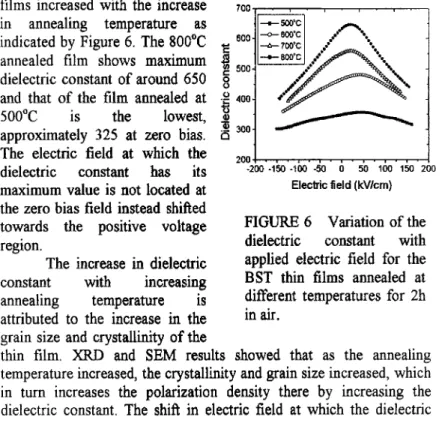
Dielectric constant of the films increased with the increase in annealing temperature as indicated by Figure 6. The 8OO0C
annealed film shows maximum dielectric constant of around 650 and that of the film annealed at 500°C is the lowest, approximately 325 at zero bias. The electric field at which the dielectric constant has its maximum value is not located at the zero bias field instead shifted towards the positive voltage region.
The increase in dielectric constant with increasing annealing temperature is attributed to the increase in the grain size and crystallinity of the
700 600
f
500 E8
.2
400a m
4
2w -200 -150 -100 -50 0 50 100 150 200 Electric field (kVlcrn)FIGURE 6 Variation of the dielectric constant with applied electric field for the BST thin films annealed at different temperatures for 2h in air.
thin film. XRD and SEM results showed that as the annealing temperature increased, the crystallinity and grain size increased, which in turn increases the polarization density there by increasing the dielectric constant. The shift in electric field at which the dielectric
constant has its maximum is because of the change in interface characteristics due to the Ti-migration, which modifies the bottom electrode interface. The space charge capacitance at the two interfaces is different because of the difference in interface characteristics.
The dielectric constant of the film prepared from the dilute solution (0.08M) is larger than that of films prepared from 0.15M and 0.28M solutions. At zero bias, the dielectric constant of the BST film prepared from 0.08M solution is around 550 where as that of 0.15 and 0.28 M solution is approximately 475. The films prepared from both 0.15 and 0.28 M solutions showed almost similar variation of dielectric constant with the bias dc-field.
Above results can be explained based on the microstructure as determined by SEM analysis. Films prepared from three different concentration precursor solutions differed in their microstructure, in- particular grain size distribution, porosity and morphology. The film prepared from the dilute solution showed lower porosity
than
that prepared from higher concentration precursor solution. This reduced porosity increases density of the film thereby increasing the polarization density, which is responsible for the increase in dielectric constant of the film prepared fiom dilute solution.CONCLUSIONS
In conclusion, Bao.sSro.sTi03 thin films can be deposited on the Pt/Ti/SiOz/Si substrate at a low temperature (500°C) using complex precursor solution prepared by using hydroxides of Ba and Sr as the Ba-, Sr- sources, Ti-isopropoxide as the Ti-source and 2-methoxy ethanol as the solvent. However, film prepared at 500°C showed high leakage current because of the presence of unburned embedded decomposition products. Reasonably good film with low leakage and high dielectric constant can be obtained after annealing at 700°C. The leakage current characteristic and the dielectric constant depend on the processing parameters such as annealing temperature, film thickness and precursor solution concentration. Another important finding of the study is the microstructure can be tailored by changing the concentration of the precursor solution. As a whole, our study highlights the intricate relationship between the film processing, microstructure and the properties of the film.
SOL-GEL DERIVED BST THIN FILMS 249
Acknowledgement
Support for this work by National Science Council of Taiwan, R.O.C. under project NSC 89-21 12-EOO9-040 is gratehlly acknowledged.
References
1. S. Ezhilvalavan and T.Y. Tseng, Mat. Chem. Phys., 65, 227 2. W.Zhu, O.K.Tan, J.Deng and J.T.Oh, J. Muter. Rex, 15, 1291 3. M.Noda, K.Hashimoto, R.Kubo, H.Tanaka, T.Mukaigawa, H.Xu
and M.Okuyama, Sens. Actua., 77,39 (1999).
4. J.G.Cheng, X.J.Meng, B.Li, J.Tang, S.L.Guo J.H.Chu, M.Wang, H.Wang and Z.Wang, Appl. Phys. Lett., 75,2132, (1999).
5. M.H. Song Y.H.Lee, T. S.Hahn, M.H.Oh and K.H.Yoon, Solid State Electronics, 42, 17 1 1, (1 998).
6. L.C.Sengupta and S. Sengupta, IEEE Trans. on Ultrasonics, Ferroelectrics and Frequency Control, 44, 792, (1997).
7. M.S. Tsai, S.C. Sun and T.Y. Tseng
, J
Appl. Phys., 82, 3482 (1997).8. M.S. Tsai, S.C. Sun and T.Y. Tseng, IEEE Transactions on Electron Devices, 46, 1829, 1999.
9. S.Saha and S.B.Krupanidhi, JAppl. Phys., 88, 3506 (2000).
10. J.H.Lee and S.W.Rhee, J.Mat. Res., 14, 3988 (1999).
11. S.B.Krupanidhi and C.J.Peng, Thin SolidFiZms, 305, 144 (1997). 12. ZABurhanuddin, M.S.Tomar and E.Dayalan, Thin Solid films, 13. D.M.Tahan, ASafari and L.C.Klein, J.Am.Ceram.
SOC.,
79, 1593, 14. B.D.Cullity, Elements of X-ray Diflaction, 2"d ed., Reading MA: 1 5 . J.O.Olowolafe, R.E. Jones Jr., A.C.Campbel1, R.I.Hegde, 16. K.Sreenivas, I. Reaney, T.Maeder and N.Setter, C.Jagadish, and(2000). (2000).
253, 53 (1994). (1 996).
Addison-Wesley, 1978, p 102.
C. J.Mogab, and R.B.Gregory, J.App1. Phys., 73, 1764 (1 993). R.G.Elliman, J.App1. Phys. 75, 232, (1994).