國 立 交 通 大 學
電信工程學系
碩 士 論 文
二種縮小化環型帶通濾波器設計
Design of Two Types of Ring-Like Bandpass
Filter with Small Size
研究生:陳殿靖
中 華 民 國 九十八 年 六 月
二種縮小化環型帶通濾波器設計
Design of Two Types of Ring-Like Bandpass
Filters with Small Size
研 究 生:
陳殿靖 Student:Dian-Jing Chen
指導教授:
張志揚 博士 Advisor:Dr. Chi-Yang Chang
國立交通大學
電信工程學系
碩士論文
A Thesis
Submitted to Department of Communication Engineering
College of Electrical and Computer Engineering
National Chiao Tung University
In Partial Fulfillment of the Requirements
for the Degree of
Master of Science
In
Communication Engineering
June 2009
Hsinchu, Taiwan, Republic of China
中華民國 九十八 年 六月
二種縮小化環型帶通濾波器設計
研究生:陳殿靖 指導教授:張志揚 博士
國立交通大學電信工程學系
摘要
本文提出兩種設計帶通濾波器的方法,第一種主要是設計一個環
型帶通濾波器並改變訊號在電路中的行徑路徑,而產生與傳統環型濾
波器一樣-270 度相位的改變,並達到縮小面積的要求。而另一種主
要是利用左手傳輸線與右手傳輸線相位響應剛好相反的特性,來設計
一個可預測傳輸零點的帶通濾波器,由於我們利用集種式元件,實際
所需要的面積非常的小。
Design of Two Types of Ring-Like Bandpass
Filters with Small Size
Student:Dian-Jing Chen
Advisor:Dr. Chi-Yang Chang
Department of Communication Engineering
National Chiao-Tung University
Abstract
The thesis discusses two novel methods to design a bandpass filter. The
first one is a dual-mode ring resonator bandpass filter where a twist
circuit is involved in the signal path to achieve a -270
ophase shift as the
as the traditional dual-mode ring resonator bandpass filter to achieve the
size reduction. The second one utilizes the feature that the phase response
of right-handed transmission lines and left-handed transmission lines are
opposite to design a bandpass filter with a predictable transmission zero.
And since we use lumped elements to implement the bandpass filter, the
size of the structure is very small.
Acknowledgement
誌謝
兩年的碩士生涯,面對了許多的挫折與失意,然而在生命中有許多的貴人幫 助我,讓我順利完成我的碩士論文。 首先,我要感謝我的指導教授 張志揚博士,在他兩年的指導中,幫助我度 過許多研究上的瓶頸,張教授在這領域淵博的知識,讓我在實驗的過程中,包括 量測,解決問題的思考上幫助良多。並且在平時相處時,與我們分享生活上的許 多趣事,讓我們的研究生活不再乏味。 其次,感謝口試委員邱煥凱教授、郭仁財教授、黃瑞彬教授,對此篇論文提 出肯切的意見。他們的指導,使本篇論文亦臻完善。 再者,要感謝所有的學長和同學。在此,更要特別感謝博班學長郭益廷,沒 有他的幫助,我很難在關鍵時刻有所突破。再來要特別感謝我的同學忠傑和昀緯, 感謝他們的陪伴和需多事情的協助。能夠在兩年的碩士生涯與這麼好的同學相處 ,讓我的生活充滿了樂趣和喜悅。 再來,要特別感謝陪伴我兩年多的 Anko,兩年來遭遇許多的挫折和無盡的 煩惱,都是你而讓我有傾訴的對象。兩年來也有許多歡樂和值得慶祝的事情, 也是你陪著我度過。我相信這些都是以後值得回味的往事吧。 最後,要感謝我的父母,你們讓我能無後顧之憂的在新竹唸書,在我心情不好時,能在電話中給我鼓勵。每個月底回家時,也能給我許多的鼓勵和叮嚀。能 夠當你們的兒子,真的很幸運。我真的很開心,能有這麼照顧我的父母。 僅將這篇論文,獻給曾經幫助過我的人們。
Contents
摘要... i
Abstract ... ii
The thesis discuss two novel methods to design a bandpass filter. The first one is a dual-mode ring resonator bandpass filter where a twist circuit is involved in the signal path to achieve a -270o phase shift as the as the traditional dual-mode ring resonator bandpass filter to achieve the size reduction. The second one utilizes the feature that the phase response of right-handed transmission lines and left-handed transmission lines are opposite to design a bandpass filter with a predictable transmission zero. And since we use lumped elements to implement the bandpass filter, the size of the structure is very small. ... ii
Acknowledgement ... iii
Contents ... v
List of Figures ... vii
List of Tables ... xii
Chapter 1 Introduction ... 1
Chapter 2 Dual-Mode Ring Resonator ... 3
2.1 Introduction ... 3
2.2 Dual-Mode Ring Resonator [1], [2], [3], [4], [7], [8], [9], [12] ... 5
2.2.1 Dual-Mode Ring Resonator [1], [2] ... 7
2.2.2 The Novel Structure of a Dual-Mode Ring Resonator Filter ... 11
2.3 Measurements and Implementation for Chip Capacitors, Tapers and Twist ... 12
2.3.2 Implementation of Tapers ... 20
2.3.3 Implementation of a -270o Section with a Twist ... 22
2.4 Design Procedure and Realization [6], [13] ... 26
Chapter 3 ... 38
3.1 Introduction ... 38
3.2 Theory [14], [15], [16], [17] ... 39
3.4 Design Procedure and Structure Analysis ... 44
3.4.1 Illustration of the Design Procedure ... 44
3.4.2 Structure Analysis ... 58
3.5 Circuit Realization and Measurements ... 64
Chapter 4 Conclusion ... 66
List of Figures
Figure 2. 1 Traditional dual-mode ring resonator with two coupling gaps. ... 5 Figure 2. 2 Magnetic-wall model for the ring resonator. ... 6 Figure 2. 3 Excitation of one of the degenerate modes. ... 6 Figure 2. 4 Structure of dual-mode resonator based on a
one-wavelength ring resonator. ... 7 Figure 2. 5 Electrical field distribution in ring. ... 8 Figure 2. 6 The response of S21 of Figure 2.4. ... 8 Figure 2. 7 Division of a dual-mode ring resonator applying an
impedance step as a perturbation. ... 9 Figure 2. 8 Equivalent circuits of a dual-mode ring resonator with
stepped-impedance type. ... 9 Figure 2. 9 Analyzing method for obtaining attenuation poles of a
dual-mode ring resonator. (a) Equivalent expression with two propagation paths. (b) Corresponding circuit expression using Y-matrices. ... 10 Figure 2. 10 Frequency responses of the impedance of an ideal
capacitor. (a) The magnitude response. (b) The phase response. ... 12 Figure 2. 11 The meanings of the part number. ... 13 Figure 2. 12 HP 4291A RF Impedance/Material Analyzer. ... 13 Figure 2. 13 (a) A complete measurement for a perturbation
measurements for four perturbation capacitors to specific frequencies (all for 8pF). ... 14 Figure 2. 14 The measurement for a external coupling capacitor to
specific frequencies (1.8pF). ... 15 Figure 2. 15 Modeling of a physical capacitor with an equivalent
circuit. ... 16 Figure 2. 16 A simplified equivalent circuit of a capacitor including
the effects of lead. ... 16 Figure 2. 17 The special designed test fixture for the measurement of the chip capacitors. ... 17 Figure 2. 18 The Bode plots of the impedance of a chip capacitor. .. 18 Figure 2. 19 The reflection coefficient S11 of the perturbation
capacitor (8pF). ... 18 Figure 2. 20 The measured input impedance of the perturbation
capacitor (8pF). ... 19 Figure 2. 21 Optimization of the equivalent circuit of the
perturbation capacitor to fit the measured one. ... 19 Figure 2. 22 The comparison between the measured and the
simulated results. ... 20 Figure 2. 23 (a) An ideal 180o transformer. (b) The simulation of (a).
... 21 Figure 2. 24 (a) The structure of a tapered-line balun, and (b) the
simulated phase response of the tapered-line balun. ... 22 Figure 2. 25 (a) The circuit model of a -270o ( 90o )section. (b) The
response. ... 24 Figure 2. 27 (a) The structure of a -270o section with a twist. (b) The
amplitude response. (c) The phase response. ... 25 Figure 2. 28 The coupling scheme of the doublet filter. ... 26 Figure 2. 29 (a) The even-mode equivalent circuit model. (b) The
simulation of (a). ... 28 Figure 2. 30 (a) The odd-mode equivalent circuit model. (b) The
simulation of (a). ... 29 Figure 2. 31 The comparison between the complete circuit model
and its 3-D structure. ... 30 Figure 2. 32 The complete circuit model with presenting its physical
length and the comparison with its 3-D structure. ... 31 Figure 2. 33 The response of the equivalent circuit model in Figure
2.32. ... 32 Figure 2. 34 (a) The final layout. (b) The simulation results of the
novel ring resonator filter. ... 33 Figure 2. 35 The photograph of the novel ring resonator filter. ... 34 Figure 2. 36 Measured and simulated S parameters of the novel ring resonator filter. (It is simulated by Sonnet.) ... 35 Figure 2. 37 Measured and simulated S parameters of the novel ring resonator filter. (It is simulated by ADS.) ... 35 Figure 2. 38 (a) Two circuit diagrams, the left one using the ideal
baluns and the right one using the tapers. (b) The simulation results of (a). ... 37
Figure 3. 2 The unit-cell equivalent circuit models for the RH and LH TLs ... 41 Figure 3. 3 The circuit diagrams and responses of S parameters of
two types of unit-cell equivalent circuits ... 43 Figure 3. 4 A simple diagram of the dual-mode ring resonator using a 90o LH TL and a -90o RH TL ... 44 Figure 3. 5 The required RH TL and LH TL ... 45 Figure 3. 6 (a) A ring-like circuit diagram composed of a 90o LH TL and a -90o RH TL (b) The response S21 of (a) ... 46 Figure 3. 7 (a) The ring-like bandpass filter composed of a 90o LH
TL and a -90o RH TL (b) The responses of (a) ... 47 Figure 3. 8 Two codes for LH and RH lumped element values
calculation ... 48 Figure 3. 9 (a) The coupling capacitance versus a series of
transmission zero (b) The fractional bandwidth versus a series of transmission zeros ... 49 Figure 3. 10 The curves for the variation of lumped element values versus a series of transmission zeros (a) For capacitance (b) For inductance ... 51 Figure 3. 11 (a) The design curve for coupling capacitance (b) The
deign curve for center frequency f0 (c) The design curve for the ration of fz/f0 (d) The design curve for fractional bandwidth (e) The design curves for capacitances of RH and LH TLs (f) The design curves for inductance of RH and LH TLs ... 54
deign curve for center frequency f0 (c) The design curve for the ration of fz/f0 (d) The design curve for fractional bandwidth (e) The design curves for capacitances of RH and LH TLs (f) The design curves for inductance of RH and LH TLs ... 58 Figure 3. 13 The even- and odd-mode equivalent circuits compared
with the original circuit ... 59 Figure 3. 14 The all responses, including Y, Z, and S parameters, of Figure 3.4.9 ... 60 Figure 3. 15 (a) The series resonant circuit (b) The parallel resonant
circuit ... 60 Figure 3. 16 The curve of K-1 ... 61 Figure 3. 17 The curve of L-1 ... 63 Figure 3. 18 The photograph of the ring-like bandpass filter
composed of a RH TL and a LH TL ... 64 Figure 3. 19 The comparison between the simulated results and the measured results ... 65
List of Tables
Table 2. 1 The coupling matrix for the doublet. ... 26 Table 2. 2 The coupling matrix of the doublet for specifications ... 27 Table 3. 1 The required element vales of CR, LR, CL, and LL………44 Table 3. 2 The phase of the input admittance of the odd-mode
equivalent circuit ... 62 Table 3. 3 The phase of the input admittance of the odd-mode
Chapter 1 Introduction
Bandpass filters used for wireless telecommunication equipment require small size in addition to low loss. Although the filter design theory has been mature and well-established, we can still reduce the area of the structure to adapt to the newest and the most stringent requirement. The techniques such as the use of high-permittivity materials, variation of resonator structure, and use of multiple resonant modes are mainly applied. Besides these well-developed techniques, we can miniaturize the size of a structure from the view by twist the signal and ground in a balanced transmission line to achieve an 180o phase shift. In order to carry out this idea, the broadside microstrip structure is used in this thesis. In Chapter 2, we will introduce such a method to fulfill the idea of reducing the area of the structure. The doublet coupling scheme will be used to illustrate this new structure.
In addition, we can miniaturize the structure by use of left-handed transmission lines (LH TL) to obtain the same phase delay but with smaller size. The left-handed transmission lines do not exist in the world naturally. Comparing with a -270o RH TL, a 90o LH TL exhibits smaller size. The lumped elements, such as chip elements, make the size of the structure smaller. However, the parasitic effects exist in the lumped elements when operation frequency is high. If we design a filter at low frequency, the parasitic effects of the lumped elements will not be so serious.
Figuring out the equivalent circuit of the lumped elements, they can be used in a relatively high frequency with more accuracy. To model a lumped capacitor by one-port S-parameter measuring will be discussed in this thesis.
Chapter 2 Dual-Mode Ring Resonator
Filter
2.1 Introduction
The ring resonator is considered a standard resonator structure for the evaluation of strip-line parameters, dielectric substrate materials, and Q-factor measurements. There are many merits such as its easy of design, excellent unloaded Q values due to low radiation loss, and no need of grounding. One interesting feature is the possibility that the TM110 resonance could be excited twice on the same physical ring thereby
implementing dual-mode microstrip ring resonators. Based on this feature, we can design a bandpass filter, which will be simply illustrated in the following paragraph.
We also contrive a novel structure to reduce the size of the traditional ring resonator filter. The proposed ring just twists the signal and ground to achieve an 180o phase shift so that the total length of the ring can be half of the traditional ring. We will detail this method in section 2.3.3. And based on this structure, we will design a dual-mode bandpass filter and analyze the structure by doublet coupling scheme. Lastly, we also introduce the measurement for the chip capacitors. Since these lumped elements are far from ideal at the operating frequency, an equivalent circuit to replace the original simple model is needed.
2.2 Dual-Mode Ring Resonator [1], [2], [3], [4], [7], [8],
[9], [12]
Figure 2. 1 Traditional dual-mode ring resonator with two coupling gaps.
Shown in Figure 2.1 is a traditional dual-mode ring resonator with two coupling
gaps. This resonator can be considered as a cavity resonator with electric walls on the top and the bottom, and magnetic walls on the side border as shown in Figure 2.2. The modes in this structure are z independent modes and have a pure longitudinal electric field, so that an Ez component is present. The magnetic field is perpendicular to the z
axis. As can be derived from Maxwell’s equations, the solutions for the field components can be written as
Ez =
{
AJn(kr)+Bn(kr)}
cos(nφ) Hr ={
( ) ( )}
sin( ) 0 φ ωµ r AJ kr BN kr n j n n n + (2.1) Hψ={
'( ) '( )}
cos( ) 0 φ ϖµ κ n kr BN kr AJ j n + n .Figure 2. 2 Magnetic-wall model for the ring resonator.
where Jn is the Bessel function of the first kind and order n, and Nn is a Bessel
function of the second kind and order n. Jn’ and Nn’ are the derivatives of the function
to the argument (kr). In (2.1), the solutions are the forms of the cosine function and the sine function dependent on the azimuthal angle ψ . This means that two degenerate modes exist at the resonant frequent. If the ring resonator without any disturbing structure considered is excited by symmetrical coupling lines, as in Figure 2.1, only one of the degenerate modes will be excited, as in Figure 2.3. Since two degenerate modes are
orthogonal to each other, no coupling occurs between the two modes.
If any perturbation is added or the symmetry of the resonator is disturbed, however two degenerate modes could be coupled. Moreover, the coupling between two degenerate modes can be used to design a dual-mode bandpass filter.
2.2.1 Dual-Mode Ring Resonator [1], [2]
Figure 2. 4 Structure of dual-mode resonator based on a one-wavelength ring resonator.
A famous configuration introduced by Mitsuo Makimoto is shown in Figure 2.4. This ring resonator consists of a one-wavelength ring resonator with an adequate perturbation placed at an equal distance from input and output ports (point C or D in the Figure). The input and output ports are spatially separated at 90o in electrical length. If there is no perturbation at C or D, no response will be generated at the output port. This phenomenon can be explained in Figure 2.5. If the electric field is excited at point ‘b’, then the maximum of the field must be at point ‘b’. Since it is a one-wavelength ring, the null of the field must be at points ‘a’ and ‘c’.
Figure 2. 5 Electrical field distribution in ring.
A simple simulation of Figure 2.4 is shown in Figure 2.6. It possesses two resonant frequencies accompanied by attenuation poles on both sides.
Figure 2. 6 The response of S21 of Figure 2.4.
Due to its symmetric geometry, the even- and odd-mode analysis can help us to explain its resonant operation. The circuit can be divided along its symmetric line as in Figure 2.7. Its even- and odd-mode equivalent circuits are shown in Figure 2.8. For the even- and odd-mode, the resonant frequencies are obtained when the input admittance of each circuit is equal to zero. By means of the parameters in Figure 2.8, two equations are presented below:
For the even mode: 0 tan tan 1+ = × p r p Z Z θ θ . (2.2) For the odd mode:
0 tan tan 1+ × p = r p Z Z θ θ (2.3)
Figure 2. 7 Division of a dual-mode ring resonator applying an impedance step as a perturbation.
Figure 2. 8 Equivalent circuits of a dual-mode ring resonator with stepped-impedance type.
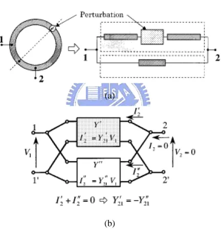
Next let us consider how to generate the attenuation poles. Shown in Figure 2.9 are the equivalent expression of the ring resonator and its corresponding Y matrix circuit. Transmission zero occurs at the frequency with the output voltage being zero. It also means that I2 becomes zero at this frequency, and the following condition is obtained.
I2’ = - I2”. (2.4)
(a)
(b)
Figure 2. 9 Analyzing method for obtaining attenuation poles of a dual-mode ring resonator. (a) Equivalent expression with two propagation paths. (b) Corresponding circuit expression using Y-matrices.
As a result, the condition to generate transmission zeros is given as
Change the length or width of the perturbation can shift the resonant frequencies and the transmission zeros. Moreover, we can use this dual-mode ring resonator with a well-designed perturbation to realize a bandpass filter. In the next section, based on this conventional configuration we design a novel dual-mode ring resonator filter to reduce the size of this traditional ring resonator filter.
2.2.2 The Novel Structure of a Dual-Mode Ring Resonator
Filter
In order to reduce the size of the ring, we must study where to consider changing the structure of the ring and how to design. Inspecting the traditional ring resonator discussed in the previous section, it is composed of a one-wavelength transmission line. If the physical length of the ring can be shortened, intuitively, the area of the ring should be reduced.
For this reason, we contrive a novel structure making use of broadside microstrip lines excited by differential signals. Furthermore, to aim at reducing the size of the ring, a twist of broadside microstrip line, which is equivalent to a 1:-1 transformer, has been implemented. In addition, to produce differential signals, a transition from the microstrip line to the broadside microstrip line working as a broadband balun must be designed. Last, for convenience, we use chip capacitors for its input and output couplings and the perturbations within the ring. In the following, the method to design these circuits will be detailed.
2.3 Measurements and Implementation for Chip
Capacitors, Tapers and Twist
2.3.1 Measurements for Chip capacitors [5]
Before implementing the measurements for chip capacitors, we first simply introduce the ideal behavior of a capacitor. The behavior of it is shown in Figure 2.10.
Figure 2. 10 Frequency responses of the impedance of an ideal capacitor. (a) The magnitude response. (b) The phase response.
The impedance is calculated as
o C C j C j j Z( )= 1 =− 1 = 1 ∠−90 ω ω ω ω . (2.6) The perturbation capacitor is a multi-layer ceramic capacitor (MLCC) produced by Murata Corp. The part number to the capacitor we use is GRM36 C0G 080D 50.
0
8 10× pF=8pF
Figure 2. 11 The meanings of the part number.
The external coupling capacitor is the chip capacitors produced by American Technical Ceramic (ATC).
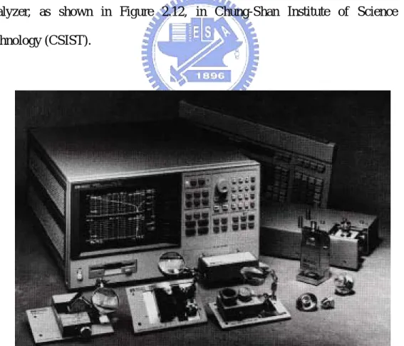
All the capacitors are firstly measured by HP 4291A RF Impedance/Material Analyzer, as shown in Figure 2.12, in Chung-Shan Institute of Science and Technology (CSIST).
The measurement data of the external coupling capacitors and perturbation capacitors are shown in Figure 2.13 (a) and (b) and Figure 2.14, respectively.
(a)
(b)
Figure 2. 13 (a) A complete measurement for a perturbation capacitor from 1.3 GHz to 1.8 GHz (8pF). (b) The measurements for four perturbation capacitors to specific frequencies (all for 8pF).
1.55 1.6 1.65 1.7 1.75 1.8 frequency(GHz) 2.13 2.14 2.15 2.16 2.17 2.18 2.19 2.2 2.21 2.22 2.23 c a p a c it a n c e (p F )
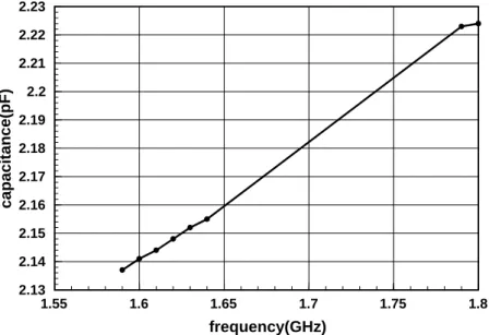
Figure 2. 14 The measurement for a external coupling capacitor to specific frequencies (1.8pF).
Apparently the characteristics of these capacitors are far from ideal, requiring that the undesirable effects such as parasitic inductance and resistance be incorporated in the design. Based on the reason, we should construct a practical equivalent circuit. Due to simplicity and the software limitation, we mainly consider the perturbation capacitors owning to their larger capacitance. The chip capacitor can be viewed as a pair of parallel plates separated by a dielectric as in Figure 2.15 with its equivalent circuit.
Figure 2. 15 Modeling of a physical capacitor with an equivalent circuit.
The loss in the dielectric is represented as a parallel resistance Rdiel. Usually, as one
would expect, this is a large value. The resistance of the plates is shown by Rplate. For
small ceramic capacitors, this is usually small enough to be neglected. The leads attached to the capacitor have parasitic Llead and Clead. Again, Clead is usually mush less
than the ideal capacitance C, and thus may be neglected. Thus the equivalent circuit is the series combination of C, Llead, and Rplate as in Figure 2.16. The impedance of this
Figure 2. 16 A simplified equivalent circuit of a capacitor including the effects of lead. model is ω ω ω ω j L R j C L L j Z lead s lead lead / ) /( 1 ) ( ˆ = − 2+ . (2.7)
The Bode plots of the impedance are shown in Figure 2.18. At dc the circuit appears as an open circuit. As the frequency increases, the impedance of the capacitor dominates and decreases linearly with frequency at a rate of -20dB/decade. The impedance of the inductor increases until it equals that of the capacitor at f0 =1/(2π LleadC). Although the magnitudes of impedances of C and Llead are
equal at f0, they are of opposite signs and appear as a short circuit. The net impedance
of the equivalent circuit is Rs. The f0 is the self-resonant frequency of the capacitor.
For higher frequency, the magnitude of the impedance of the inductor dominates and the impedance increases, while the phase angle approaches +90o. Furthermore, for a fixed lead length and spacing, the larger the capacitance is the lower the self-resonant
frequency will be.
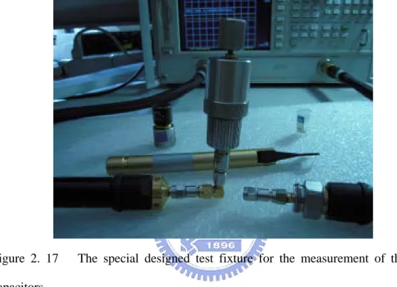
With the help of CSIST, we use the special designed test fixture which is suitable for high frequency measurement of these chip type lumped elements, as in Figure 2.17.
Figure 2. 17 The special designed test fixture for the measurement of the chip capacitors.
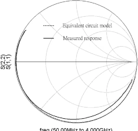
The reflection coefficient S11 of the perturbation capacitor, labeled as 8pF, is
represented in the Smith Chart as shown in Figure 2.19. The curve circled by the red ellipse represents that the magnitude of the impedance has been dominated by the inductor, Llead. The frequency at m1, i.e. the self-resonant frequency, can also be seen
Figure 2. 18 The Bode plots of the impedance of a chip capacitor.
Figure 2. 20 The measured input impedance of the perturbation capacitor (8pF).
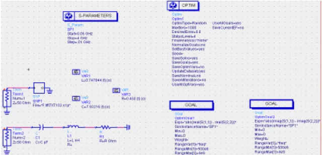
We can use the commercial simulation solver Agilent Advanced Design System (ADS) to extract the element values of the equivalent circuit in Figure 2.21. Finally, the measured result is compared with the simulated one in Figure 2.22. The values of the Rplate, Llead,and C, after extraction, are 0.45 Ohm, 0.74784 nH, and 7.93216 pF,
respectively. The capacitance is 7.93216 pF, which is very close to the labeled value, 8pF.
fit the measured one.
Figure 2. 22 The comparison between the measured and the simulated results.
2.3.2 Implementation of Tapers
The input and output of our proposed filter are microstrip lines. However, the ring should be excited by the broadside microstrip line, which is a balanced transmission line. During the circuit simulation, the transformer is used as an ideal balun and the broadside microstrip line can be represented by two back-to-back connected microstrip line with half of the broadside microstrip line impedance as shown in Figure 2.23 (a) and (b).
(a)
Figure 2. 23 (a) An ideal 180o transformer. (b) The simulation of (a).
However, such an ideal transformer is hardly achieved. A taper structure as shown in Figure 2. 24(a) can be used to realize a transformer. The simulated results of this tapered-line balun are shown in Figure 2. 24(b). Obviously, there is a 10o~11o phase imbalance.
(a)
(b)
Figure 2. 24 (a) The structure of a tapered-line balun, and (b) the simulated phase response of the tapered-line balun.
2.3.3 Implementation of a -270
oSection with a Twist
Figure 2.25(a) and (b) show the ADS circuit model and the simulated result of the twist line section.
(a)
(b)
Figure 2. 25 (a) The circuit model of a -270o ( 90o )section. (b) The phase response.
In order to implement a -270o section, we roughly partition this section into two parts, namely, a -90o section and a -180o section. The 1:-1 transformer is intended to be realized by using a structure of twist, which is short in physical size.
Shown in Figure 2.26 are a -90o broadside microstrip line and its phase response. Now a twist with two sections of broadside microstrip lines connecting with its both
Figure 2. 26 A -90o broadside-coupled transmission line and its phase response.
sides are designed. Initially, the length of the structure is made the same as that of the -90o broadside microstrip line. In the equal physical length situation, the phase response at f0 is smaller than -270o (or smaller than 90o). Decreasing the length of the
structure increases the electrical length. After fine tuning, the required -270o (or 90o) structure is obtained. Its amplitude and phase responses are shown in Figure 2.27.
(a)
(b)
(c)
Figure 2. 27 (a) The structure of a -270o section with a twist. (b) The amplitude response. (c) The phase response.
2.4 Design Procedure and Realization [6], [13]
We want to design a dual-mode bandpass filter with the following specifications: 1. Center frequency = 1.62GHz
2. Fractional bandwidth = 17%
3. Return loss at the center frequency = 20dB
The doublet coupling scheme as shown in Figure 2.28 is used to implement the dual- mode filter.
Figure 2. 28 The coupling scheme of the doublet filter.
‘S’ stands for source, ‘L’ for load, ‘e’ for even mode, and ‘o’ stands for odd mode. The corresponding coupling matrix M, according to Figure 2.28, can be written as
Table 2. 1 The coupling matrix for the doublet.
0 Mse Mso 0
Mse Mee 0 MeL
Mso 0 Moo MoL
0 MeL MoL 0
After numerical synthesis, we have the corresponding coupling matrix M as shown in Table 2.2.
Table 2. 2 The coupling matrix of the doublet for specifications
0 0.866 -0.866 0 0.866 1.658 0 0.866 -0.866 0 -1.658 0.866 0 0.866 0.866 0
An important property of the scheme in Figure 2.28 is that one of the coupling coefficients on the two main paths must be negative while the other is positive. By means of the coupling matrix, we use the commercial simulation solver Advanced Design System (ADS) of the Agilent Inc. to realize the circuit model first. For the even mode, we try to fine tune the values of the elements in the circuit to fit Mse. The
circuit diagram and its simulated result are shown in Figure 2.29(a) and (b). The Qex
(b)
Figure 2. 29 (a) The even-mode equivalent circuit model. (b) The simulation of (a).
is calculated as following: 0975 . 24 2 ) 425 . 1 548 . 1 ( 482 . 1 2 _ 3 0 × = − = × = bandwidth dB f Qex (2.4)
and the Mse, then, is calculated as: (ffractional =0.065)
8 . 0 065 . 0 1 0975 . 24 1 1 1 − = × = × = − fractional ex se f Q M , (2.5) which is close to the value of Mse in Table 2.2. For the odd mode, in the same way as
we do for even mode, the circuit diagram and its simulation are shown in Figure 2.30 (a) and (b). The Qex, again, is calculated as following
71 . 0 065 . 0 1 5636 . 30 1 = × = so Q (2.6) and the Mso is calculated as
71 . 0 065 . 0 1 5636 . 30 1 × = = so M (2.7)
(a)
(b)
Next, we explain how to realize the circuit model in our proposed novel structure. First, the circuit model corresponding to the 3-D structure is shown in Figure 2.31. The basic operating theorems of the twist and the taper, which is to realize a transformer, have been introduced in the previous section.
Figure 2. 31 The comparison between the complete circuit model and its 3-D structure.
Now, we begin to implement the whole bandpass filter.
obtain the physical length of each section. The entire circuit was manufactured on a Rogers RO4003 substrate with εr =3.58 and thickness of 20mil. The complete
circuit model with presenting its physical length of each section and the comparison with its 3-D structure is shown in Figure 2.32. We at first use ADS to simulate the
Figure 2. 32 The complete circuit model with presenting its physical length and the comparison with its 3-D structure.
the circuit above. The response is shown in Figure 2.33. Lastly, we utilize the EM software
Figure 2. 33 The response of the equivalent circuit model in Figure 2.32.
Sonnet of Sonnet Inc. to complete the simulation. After fine tuning, the physical dimensions of the novel ring resonator filter are acquired. Figure 2.34 (a) and (b) indicate the final layout and simulation results under metal loss condition, respectivily. Note that the perturbation capacitors have been replaced by their equivalent circuits discussed in the previous section.
(a)
Figure 2.35 illustrates the photograph of the novel ring resonator filter. The entire circuit is manufactured on substrate with εr =3.58 and of thickness 20 mil and the thickness of metal is 0.7 mil. Both simulated and experimental results of the frequency response of the novel dual-mode ring resonator are shown in Figure 2.36. The comparison between the simulated results by circuit model and the measured results are in Figure 2.37.
The front The back Figure 2. 35 The photograph of the novel ring resonator filter.
Figure 2. 36 Measured and simulated S parameters of the novel ring resonator filter. (It is simulated by Sonnet.)
Figure 2. 37 Measured and simulated S parameters of the novel ring resonator filter. (It is simulated by ADS.)
Now we have to explain some important features in the measured results. First, there is a peak at the lower frequency. This is because the taper is not an ideal balun, which has been discussed in the previous section. In order to prove this reason, we compare the following two circuit diagrams and their simulations as in Figure 2.38(a) and (b). The file is obtained from the EM simulation of the tapered-line balun as illustrated in the previous section. Second, there is a transmission at the higher frequency in the Sonnet simulation. This is due to fine tune of the length of the line and the capacitance. The measurement results, however, shows blurry phenomenon of the transmission zero.
(b)
Figure 2. 38 (a) Two circuit diagrams, the left one using the ideal baluns and the right one using the tapers. (b) The simulation results of (a).
Chapter 3
3.1 Introduction
Recently, left-handed materials have gained significant attention in the microwave community. And many researchers have been described and concerned with the applications of the left-handed materials such as left-handed transmission lines (LH TLs). There are many merits of the LH TLs. They can be made small and has a mild frequency dependence of phase response around the frequency of interest.
In this chapter, we will utilize both the right-handed transmission lines (RH TLs) and the left-handed transmission line to design a bandpass filter with the predictable transmission zero. And we also introduce the general design method to implement the bandpass filter.
3.2 Theory [14], [15], [16], [17]
Left-handed (LH) materials were first investigated theoretically by Veselago in 1968. As these materials have been known, they are characterized by simultaneously negative permittivity and permeability. Now let us try to explain why these materials are called left-handed materials. To answer this question, it must turn to the Maxwell equations and the constitutive relations:
E D H B t D H t B E K K K K K K K ε µ = = ∂ ∂ − = × ∇ ∂ ∂ − − = × ∇ . (3.1)
For a plane monochromatic wave, in which all quantities are proportional to e-(kz-wt), the above equations reduce to
E H k H E k K K K K K K ωε ωµ − = × = × . (3.2)
It can be understood from these equations that if ξ>0 and μ>0, then E, H and k form a right-handed triplet of vectors. In contrast, if ξ<0 and μ<0, they constitute a left-handed set. We can use Figure 3.1 to illustrate this concept with the thumb standing for the direction of HK .
Figure 3. 1 The directions of k, E and H for RH and LH materials.
Another property of LH TLs is their negative propagation constant. Due to this property, their phase responses are advance not delay. The propagation constants of RH and LH TLs are 0 1 0 < − = > = L L L R R R C L C L ω β ω β . (3.3)
The group delay of RH and LH TLs are also calculated as LH : ( ) 12 ω ω β ω ϕ =+ = × − = L L p C L l d l d d d t (3.5) RH : p R R l CRLR d C L l d d d t =− =− =− ω ω ω ϕ ( ) . (3.6) Obviously to RH TLs, the group delay is a negative constant; however, to LH TLs, the group delay has1/ω2 dependence. Dispersion becomes larger as the frequency decreases.
According to the explanation above, we construct unit-cell equivalent circuit models for RH and LH TLs as depicted in Figure 3.2 (a) and (b).
(a)
(b)
Figure 3. 2 The unit-cell equivalent circuit models for RH and LH TLs.
There are two different unit-cell types and each of them has different responses. For the unit-cell type in Figure 3.2 (a), the phase responses can be expressed as
0 ] 2 1 ) / ( arctan[ 0 ] 2 ) / ( arctan[ 2 0 0 2 0 0 > − + − = < − + − = L L L L L L L R R R R R R R C L Z C Z L C L Z C Z L ω ω ϕ ω ω ϕ (3.7) where 0 R R R L Z C = (3.8) and 0 L L L L Z C = (3.9)
are the characteristic impedances of RH and LH TLs, respectively. The phase responses of the unit cells in Figure 3.2 (b) are
(
)
(
)
] 0 2 1 4 1 arctan[ 0 ] 2 4 arctan[ 2 0 2 0 0 2 0 2 2 0 0 > − − + − = < − − + − = L L L L R R R L L R R R R R R R R R R L C Z C Z L Z C L C Z L C Z L Z C ω ω ω ϕ ω ω ω ϕ . (3.10)For both cases, their amplitude and phase responses are somewhat different. To LH TLs, for example, let o
L =45
ϕ . The circuit diagrams and responses are shown in Figure 3.3. It is obvious that the unit cells in Figure 3.2 (b) are better than that in Figure 3.2 (a).
(a)
(c)
Figure 3. 3 The circuit diagrams and responses of S parameters of two types of unit-cell equivalent circuits.
Because of the explanation discussed above, the unit cells in Figure 3.2 (b) are chosen to design the bandpass filter .
3.3 Dual-Mode Ring Resonator Using a 90
oLH TL
and a -90
oRH TL
If we want to design a bandpass filter with the predictable transmission zero, it should be identified that at the frequency of the transmission zero, the signals should cancel each other at the output. We address a simple diagram to outline the idea for designing thebandpass filteras in Figure 3.4.
Figure 3. 4 A simple diagram of the dual-mode ring resonator using a 90o LH TL and a -90o RH TL.
At point A, the signals from two paths, +90o LH TL and -90o RH TL, will cancel each other at point A since their phase difference is just 180o. The next section will discuss the design procedure of the bandpass filter.
3.4 Design Procedure and Structure Analysis
3.4.1 Illustration of the Design Procedure
We now take an example to illustrate how to design a bandpass filter composed of a 90o LH TL and a -90o RH TL.
At first, we suppose that the location of the transmission zero can be at 300MHz and the characteristic impedance of both LH TL and RH TL is 50 Ohm. Based on this specification, utilize the equations (3.8) and (3.9), and we can obtain the following relationships R R C L = 2500× (3.11) and R L C L = 2500× . (3.12)
Substitute the relationships above for the LR and LL in equations (3.10), and let o 90 − = ϕ and o L =90
ϕ . After tedious calculation, we obtain Table 3. 1 The required element vales of CR, LR, CL, and LL
Note that sincecot(±90o)=0, equations in (3.7) and (3.10) can obtain the same results. Making use of the T-type unit-cell equivalent circuits of RH and LH TLs in Figure 3.2(b), we obtain the following results as in Figure 3.5.
Figure 3. 5 The required RH TL and LH TL.
Now, connect the LH and RH TL to form a ring-like configuration and direct connect to the source and load without external coupling capacitors. The circuit diagram and the simulated result are shown in Figure 3.6 (a) and (b), respectively. At 300MHz, there is a transmission zero as we supposed.
(b)
Figure 3. 6 (a) A ring-like circuit diagram composed of a 90o LH TL and a -90o RH TL. (b) The response S21 of (a).
Now we add the two external coupling capacitors and increase the values. Since this is a symmetric structure, the values of the two coupling capacitors keep the same. In order to achieve a systematic design method, we secondly specify the return loss to be -20 dB. To fulfill the specification, we fine tune the values of two coupling capacitors. The circuit diagram and the simulated results are depicted in Figure 3.7 (a) and (b). The return loss at the center frequency is -20 dB as we specify. The center frequency of this example is at 271.3 MHz and the fractional bandwidth is calculated as 8708 . 14 % 100 3 . 271 8 . 245 1 . 286 = × − . (3.13)
(a)
Figure 3. 7 (a) The ring-like bandpass filter composed of a 90o LH TL and a -90o RH TL. (b) The responses of (a).
characteristic impedances, we construct a series of tables in regard to 25 Ohm , 50 Ohm and 75 Ohm. Constructing a series of tables, however, is a wearisome work; therefore, simple codes to calculate the values of these lump elements are in urgent need. The following presents two codes for LH and RH lumped element values calculation as in Figure 3.8.
Figure 3. 8 Two codes for LH and RH lumped element values calculation.
After precise and routine calculations, we obtain a series of design curves. First we consider the results for characteristic impedance of 50 Ohm. The design curves are in Figure 3.9 (a) and (b). In (a) shows a coupling capacitance versus series of trans-
(b)
Figure 3. 9 (a) The coupling capacitance versus a series of transmission zeros. (b) The fractional bandwidth versus a series of transmission zeros.
mission zeros , while Figure 3.9 (b) is a curve for the fractional bandwidth versus location of the transmission zeros. Figure 3.10 (a) and (b) present the 50 Ohm LH and RH TL element values with respect to location of the transmission zeros. With the transmission zeros from 200 MHz to 400 MHz, observe the relations between these element values. The lumped element values decrease as the frequency of the transmission zero increases.
Figure 3. 10 The curves for the variation of lumped element values versus the location of transmission zero. (a) For capacitance. (b) For inductance.
Next, we present the design curves for the characteristic impedance of 25 Ohm and 75 Ohm as in Figure 3.11 and 3.12, respectively.
For 25Ω :
(b)
(d)
(f)
Figure 3. 11 (a) The design curve for coupling capacitance. (b) The deign curve for center frequency f0. (c) The design curve for the ration of fz/f0. (d) The design curve
for fractional bandwidth. (e) The design curves for capacitances of RH and LH TLs. (f) The design curves for inductance of RH and LH TLs.
(a)
(c)
(e)
Figure 3. 12 (a) The design curve for coupling capacitance. (b) The deign curve for center frequency f0. (c) The design curve for the ration of fz/f0. (d) The design curve
for fractional bandwidth. (e) The design curves for capacitances of RH and LH TLs. (f) The design curves for inductance of RH and LH TLs.
Last we make a short conclusion. As we choose the smaller value of the characteristic impedance, the larger the capacitance and the smaller the inductance for both RH and LH unit cell will be. Among 200 MHz to 400 MHz, the variation of the fractional bandwidth is very small and the ratio, fz /f0, is nearly a constant.
3.4.2 Structure Analysis
The symmetrical geometry of the structure allows us to explain its resonant operation by the even- and odd-mode analysis. Since the circuit composed by RH and LH TLs without external coupling capacitors shows no dual-mode response as in Figure 3.6 (b), the external coupling capacitors must be considered in the even- and odd-mode analysis.
For the even mode, the circuit is divided into one-half at the symmetric plane, where the values of lumped elements should be modified by virtue of the circuit theorems. For an odd mode, since it is short circuit at the symmetric plane, the equivalent circuit becomes very simple. The even- and odd-mode equivalent circuits are shown in Figure 3.13. And small capacitance of the two coupling capacitors is applied for convenient observation of their responses. The responses, including Y-, Z-, and S parameters, of Figure 3.13 are shown in Figure 3.14 (a) to (c).
Figure 3. 13 The even- and odd-mode equivalent circuits compared with the original circuit.
Figure 3. 14 The all responses, including Y-, Z-, and S-parameters, of Figure 3.13.
The following paragraphs will explain these results.
Figure 3.14 (a) and (b) implicate that the even- and odd-mode equivalent circuits are the series resonant circuits. We can illustrate this result by the following simple and basic series and parallel resonant circuits as in Figure 3.15 (a) and (b), respectively. For a series resonant circuit, the input admittance shows a peak at the resonant frequency. For a parallel resonant circuit, inversely, it is the input impedance that shows a peak at the resonant frequency.
(a)
(b)
Figure 3. 15 (a) The series resonant circuit. (b) The parallel resonant circuit.
Now we attempt to understand the phase change in Figure 3.14 (c). For the odd-mode equivalent circuit in Figure 3.13, the input impedance is
) ( ) 1 ( ) 1 ( 1 ) 1 ( 1 c c c in C L C L C C j C j L C j Z ω ω ω ω ω ω ω ω ω − − × + + = + − = , (3.14)
where Cc represents the coupling capacitance of the odd-mode equivalent circuit. The
phase of Zin, which is either +90o or -90o, is determined by the polarity of the part, K:
K= ) ( ) 1 ( ) 1 ( c c C L C L C C ω ω ω ω ω ω × − − + − . (3.15)
The phase of Yin, of course, is decided by the reciprocal of K. With a simple code, we
can easily observe the change of the value of the reciprocal of K (i.e. K-1). The result is shown in Figure 3.16. The zeros of K-1 are at 296.8 MHz and 300 MHz, which fits the result in Figure 3.14 (c). According to the result, we construct a table for convenience.
Figure 3. 16 The curve of K-1.
equivalent circuit. The result matches the phase change simulated in Figure 3.14 (c). For the even-mode equivalent circuit in Figure 3.13, as we do for the even-mode Table 3. 2 The phase of the input admittance of the odd-mode equivalent
circuit
f < 296.8MHz 296.8MHz < f < 300MHz 300MHz < f K-1 < 0 > 0 < 0
K-1*(-j) 90o -90o 90o
Yin 90o -90o 90o
equivalent circuit, the input impedance is
] 1 ) 2 1 2 ( ) 1 ( ) 2 1 2 ( ) 1 ( [ c in C C L C L C L C L j Z ω ω ω ω ω ω ω ω ω − − + − − × − = . (3.16)
The phase of Zin is determined by the polarity of the part, L:
L = 1 ] ) 2 1 2 ( ) 1 ( ) 2 1 2 ( ) 1 ( [ c C C L C L C L C L ω ω ω ω ω ω ω ω ω − − + − − × − . (3.17)
The phase of Yin, of course, is decided by the reciprocal of L. The result is shown in
Figure 3.17 . The zeros of L-1 are at 298.9 MHz and 300 MHz., which also matches the result in Figure 3.14 (c). Table 3.3 also arranges the phase change of the input
Figure 3. 17 The curve of L-1.
admittance of the even-mode equivalent circuit, which also fits the result in Figure 3.14 (c).
Table 3. 3 The phase of the input admittance of the odd-mode equivalent
circuit
f < 298.9 MHz 298.9 MHz < f < 300 MHz 300MHz < f L-1 < 0 > 0 < 0
L-1*(-j) 90o -90o 90o
3.5 Circuit Realization and Measurements
We use the example, in section 3.4.1, to realize and measure the circuit. The photograph of the circuit is shown in Figure 3.18. The entire circuit was manufactured on substrate with εr =3.58 and of thickness 20 mil and the thickness of metal is 0.7 mil. The inductors are implemented by coiling the coated thin copper wires and we measure the inductance with the equipment as we do for measuring the capacitance. However, the inductance is difficult to maintain, since the thin copper wires are easily to be bended.
Both simulated and experimental results of the frequency response of this bandpass filter are shown in Figure 3.19. Note that the simulated results in Figure 3.19 are completed by ADS.
Figure 3. 18 The photograph of the ring-like bandpass filter composed of a RH TL and a LH TL.
Figure 3. 19 The comparison between the simulated results and the measured results.
Chapter 4 Conclusion
In this thesis, a novel structure of broadside-coupled ring resonator for bandpass filter application and a bandpass filter composed of a RH and LH TLs have been completed. Although there are some parasitic inductance and resistance in a capacitor, we have endeavored to solve the problem by constructing its equivalent circuit model. The taper to realize an ideal balun has its imbalance and this imbalance generates undesired responses at the lower frequency, which we have make effort to explain it. The use of structure of the twist and the lumped elements to realize a RH and LH TLs are successful in reducing the size of the filter. The use of RH and LH TLs to construct a bandpass filter, particularly, simplify the manufacturing process and can easily predict the desired frequency of the transmission zero. These two types of bandpass filter are easy to change its response to fulfill some requirement since we can arbitrarily replace these lumped elements with the new elements we desire. These are the most attractive merits of the two proposed structure.
Reference
[1] J. S. Hong and M. J. Lancaster, Microstrip Filters for RF/Microwave Applications, New York: Wiley, 2001.
[2] Rajesh Mongia, Inder Bahl, Prakash Bhartia, RF and Microwave Coupled-Line
Circuits, London: Artech House, 1999.
[3] George D. Vendelin, Anthony M. Pavio, Ulrich L. Rohde, Microwave Circuit
Design Using Linear and Nolinear Techniques, New York: Wiley, 1990. [4] D. Pozar, Microwave Engineering, 3rded. New York: Wiley, 2005.
[5] Clayton R. Paul, Introduction to Electromagnetic Compatibility,2nd ed. New York: Wiley, 2006.
[6] Richard J. Cameron, Chandra M. Kudsia, Raafat R. Mansour, Microwave Filters
for Communication Systems, New York: Wiley, 2007.
[7] Michiaki Matsuo, Hiroyuki Yabuki, and Mitsuo Makimoto, “Dual-Mode Stepped-Impedance Ring Resonator for Bandpass Filter Applications,” IEEE
Trans. Microwave Theory Tech., vol. 49, no. 7, pp. 1235-1240, July. 2001.
[8] M. Guglielmi and G. Gatti, “Experimental Investigation of Dual-Mode Microstrip Ring Resonators,” European Space Research and Technolody Centre., Po Box 299,2200AG, Noordwijk, The Netherlands.
[9] I. Wolff, “Microstrip Bandpass Filter Using Degenerate Modes of a Microstrip Ring Resonator,” Electronics Letters., vol. 8, no. 12, pp. 302-303, June 1972. [10] I. Wolff and N. Knoppik, “Microstrip Ring Resonator And Dispersion
Measurement on Microstrip Lines,” Electronics Letters., vol. 7, no. 26, pp. 779-781, June 1971.
Communication, Springer, 2000.
[13] Ching-Ku Liao, Pei-Ling Chi, and Chi-Yang Chang, “Microstrip Realization of Generalized Chebyshev Filters With Box-Like Coupling Schemes,” IEEE Trans.
Microwave Theory Tech., vol. 55, no. 1, pp. 147-153, Jan. 2007
[14] V. G. Veselago, “The Electrodynamics of Substances with Simultaneously Negative Values of ε and µ ,” Sov. Phys,-Usp., vol.10, no. 4, pp.509-514,Jan.-Feb, 1968.
[15] Hiroshi Okabe, Christophe Caloz, and Tatsuo Itoh, “A Compact Enhanced-Bandwidth Hybrid Ring Using an Artificial Lumped-Element Left-Handd Transmission-Line Section,” IEEE Trans. Microwave Theory Tech., vol. 52, no. 3, pp. 798-804, Mar. 2004.
[16] I-Hsiang Lin, Marc Devincentis, Christophe Caloz, and Tatsuo Itoh, “Arbitrary Dual-Band Components Using Composite Right/Left-Handed Transmission Lines,” IEEE Trans. Microwave Theory Tech., vol. 52, no. 4, pp. 1142-1149, Apr. 2004.
[17] K. Srisathit, P. Jadpum, S. Bunnjaweht, and W. Surakampontorn, ”New Dual-Mode Ring Bandpass Filter Using Symmetrical Left-Handed Transmission Line,” APMC 2007.