國立交通大學
照明與能源光電研究所
碩士論文
二氧化鈦奈米管陣列與複合結構在染料敏化太陽
能電池之應用
Dye-Sensitized Solar Cell using TiO
2Nanowires on
Anodic TiO
2nanotube Arrays (TNWs/TNAs)
研 究 生:楊雅婷
指導教授:呂志鵬 博士
二氧化鈦奈米管陣列與複合結構在染料敏化太陽能電池之應用
Dye-Sensitized Solar Cell using TiO2 Nanowires on Anodic TiO2
nanotube Arrays (TNWs/TNAs)
研 究 生:楊雅婷 Student:Ya-Ting Yang
指導教授:呂志鵬 教授
Advisor:Dr. Jihperng Leu
楊界雄 教授
Dr. Kei-Hsiung Yang
國立交通大學
照明與能源光電研究所
碩士論文
A Thesis
Submitted to Institute of Lighting and Energy Photonics
College of Photonics
National Chiao Tung University
in partial Fulfillment of the Requirements
for the Degree of
Master
in
Lighting and Energy Photonics
September 2012
Hsinchu, Taiwan, Republic of China
二氧化鈦奈米管陣列與複合結構在染料敏化太陽能電池之應用
研究生:楊雅婷 指導教授:呂志鵬 博士
楊界雄 博士
國立交通大學
照明與能源光電研究所
摘 要
染 料 敏 化 太 陽 能 電 池 (D ye -s ensit ized sol ar cell , DSS C) 是 目 前 極 具 發 展 潛 力 的 新 一 代 有 機 太 陽 能 電 池 。 其 中 光 電 極 表 面 形 貌 是 影 響 效 率 的 主 因 之 一 , 期 望 利 用 二 氧 化 鈦 奈 米 管 一 維 陣 列 結 構 改 善 電 子 傳 輸 而 提 升 效 率 且 未 來 發 展 可 饒 式 元 件 具 有 較 高 的 穩 定 性 。 本 論 文 中 , 含 乙 二 醇 , 氟 化 銨 及 含 水 之 電 解 液 以 陽 極 氧 化 處 理 法 , 於 鈦 板 製 備 二 氧 化 鈦 奈 米 陣 列 (TNAs) 及 其 複 合 結 構 (TNWs/TNAs) 薄 膜 層 上 。 實 驗 中 由 電 壓 、 時 間 及 攪 拌 對 於 結 構 變 化 關 係 可 推 論 其 形 成 機 制 並 利 用 其 變 化 製 作 相 同 厚 度 薄 膜 , 但 不 同 形 貌 之 二 氧 化 鈦 光 電 極 。 進 而 探 討 不 同 電 壓 時 間 ,產 生 不 同 結 構 TNAs 及 TNWs/TNAs。進 而 應 用 於 染 料 敏 化 太 陽 能 電 池 光 轉 換 效 率 影 響 。 由 光 電 轉 換 效 率 及 可 見 光 光 譜 儀 檢 測 在 相 同 膜 厚 (12µ m) , 奈 米 線 複 合 結 構 染 料 吸 附 量 較 僅 奈 米 管 結 構 來 的 多 , 透 過 提 升 吸 附 染 料 而 提 高 光 電 流 密 度 , 而 有 較 好 的 光 電 轉 換 效 率 。 於 30 伏 特 電 壓 下 製 備 8 小 時 之 二 氧 化 鈦 複 合 結 構 染 料 吸 附 相 對 純 奈 米 管 結 構 有 21%的 差 異 且 轉 換 效 率 達 η=1.85%,其 中 電 流 密 度 由 3.80 提 高 至 5.27 (mA/cm2 ) 。
Dye-Sensitized Solar Cell using TiO2 Nanowires on Anodic TiO2
Nanotube Arrays (TNWs/TNAs)
Student: Ya-Ting Yang Advisor: Dr. Jihperng (Jim) Leu Dr. Kei-Hsiung Yang
Institute of Lighting and Energy Photonics College of Photonics
National Chiao Tung University
ABSTRACT
Dye-sensitized solar cell (DSSC), a new generation solar cell, has the potential to be widely used due to its advantages of low cost, compatibility for flexible devices, and enhanced performance with temperature. Specifically, the morphology of TiO2 film is
one of the major factors affecting the conversion efficiency. Among various structures, TiO2 nanotube has great potential due to the highly ordered could provide a direct
transport route and higher stability for flexible device.
In this study, a TNWs/TNAs hybrid structure was first fabricated using a one-step method by anodizing a titanium foil in electrolytes consisting of NH4F and H2O, under
different voltage and processing time. The evolution and the mechanism of TNWs/TNAs hybrid structure prepared by using mechanical stirring were examined and proposed. The DSSC performance of TNWs/TNAs was measured and compared to TNAs and conventional TiO2 nanoparticle film. Based on the I-V characteristics and
dye absorption measurement by an UV-visible spectroscopy, nanowires in the TNWs/TNAs (12 m) hybrid structure enhance the surface area and improve the redox couple diffusion in Ti O2 el ect rode t o rai s e the photocurrent , resulti ng i n
enhanced conversi on effi ci ency. For TNW s/TNAs h ybrid st ruct ure ( 30V, 8 hours ), the conversion effi ci enc y and Js c are 1.85%, 5.27 mA/cm2, compared
to 1.04% and 3.81 mA/cm2 in a TNA only film. The 44.3% improvement in conversion efficiency can be attributed to the enhanced dye adsorption (21%) and better electron transport in TNWs/TNAs compared to TNAs only. Overall, TNWs/TNAs films show great potential to be a simple and flexible DSSC.
Acknowledgements
很榮幸能夠進入交大光電學院就讀碩士學位,在台南校區的時光雖不長卻與 同伴有著深厚的情誼 ◦ 感謝楊界雄老師在台南校區時的教學以及照顧,進入呂志 鵬老師實驗室後,非常感謝老師在各實驗方向上的提點,且在論文內容上對我的 引導跟指正◦ 在碩士期間,老師除了提供實驗上的支持,同時為增進實驗室成員 們的情誼也舉辦了很多活動,讓這段研究所時光充滿了許多回憶◦ 每周的會議上,老師總會對於報告提出意見:教導應具備的邏輯思維、檢討實 驗步驟及對實驗環境安全的提點◦促使我們能夠更加細心及注意的檢視進而改進◦ 進入實驗室,非常感謝各位熱心的學長姊 ◦無論是實驗室事務的交接還是實 驗上的承襲都受益良多 ◦ 其中明義學長及幸鈴學姊是使我能夠畢業的最大功臣, 實驗上的帶領以及面對問題時的解惑,學長姐們總是能夠給我一個很好的方向及 答案◦ 一方面也教導我資料應該如何整理、文獻應該如何去研讀等等事情都能透 過與各位學長姊的談話中,獲得了不少啟發◦ 同儕之間,維剛在我有需要幫助時,總是義不容辭的給予支援及意見,且總能夠 在談話中獲得許多不同領域的知識◦在丞芳的陪同下,我們總是歡樂的一同做著實 驗,即使是面對挫折也能夠一同商討互相打氣◦ 龍哥、王智及大龜學長們的幽默常常讓整個實驗室氣氛活絡而弘恩學長總是不 厭其煩的代為操作 FIBSEM,真的相當的感謝◦ 也感謝上一屆的學長:小胡 、阿爆、 沁穎及書豪們的實驗經驗分享以及學妹麒雅在實驗上的支援與幫助◦透過 認識大家而增長見聞,一起度過了在交大的校園時光◦ 另外要感謝軍華實驗室的政衡, 因為有你的幫助實驗才能夠順利的進行 ◦ 而好友炫文及冠名總在我失落或是熬夜時刻,以簡訊打電話的方式不斷提醒要我 保重身體◦ 不斷鼓勵我和聽我抱怨,真的非常的感動能有這樣的摯友◦ 最後,我要由衷感謝我的家人讓我在這樣無憂無慮的環境下,一路學習至今 並且總是支持我的決定及想法,感謝你們的付出及陪伴◦Contents
摘 要 i
ABSTRACT ... ii
Acknowledgements ... iv
Contents v Table Captions ... vii
Figure Captions ... viii
Chapter 1 Introduction ... 1
1.2 Overview ... 3
Chapter 2 Literature Review ... 6
2.1 Dye-sensitized Solar Cell ... 6
2.1.1 The Structure and Working Principle of DSSC [1] ... 6
2.1.2 Operation Principles of Dye-sensitized Solar Cells ... 8
2.2 Components of DSSCs ... 9
2.2.1 Substrate... 9
2.2.2 Nanocrystalline Photo-anode ... 10
2.2.3 The Sensitizer: Organic dye ... 11
2.2-4 Electrolyte... 13
2.2.5 Counter electrode ... 16
2.2.6 Sealant and Spacer ... 17
2.2.7 Post-treatment/Pretreatments/Underlayer ... 17
2.3 Anodic oxidization technique ... 19
2.3.1 The development of anodized TiO2 nanotubes ... 19
2.3.2 The growth of TiO2 nanotube: fundamental aspects ... 20
2.3.3 Key parameters for controlling the growth of the nanotubes ... 22
2.3.4 Application on DSSCs of TiO2 nanotubes arrays ... 23
2.3.5 Challenge of TiO2 nanotubes arrays on DSSCs ... 24
2.3.6 TiO2 hybrid structure (TNWs/TNAs) ... 24
2.3.7 Anneal treatment for TiO2 material ... 25
3.1 Materials ... 40
3.2 TiO2 films Preparation ... 42
3.2.1 TiO2 nanotube arrays film (TNAs) ... 42
3.2.2 TiO2 hybrid film (TNWs/TNAs)... 42
3.2.3 Post-treatment for TiO2 films ... 43
3.3 DSSC fabrication ... 43
3.4 Characterization techniques ... 44
3.4.1 Morphology and microstructure characterization of TiO2 nanostructure ... 44
3.4.2 Dye adsorption measurement... 44
3.4.3 Conversion Efficiency ... 45
3.5 Experimental flow ... 45
Chapter 4 Results and Discussion ... 49
4.1 Influence of anodization parameters ... 49
4.1.1 Influence of anodizing voltage and processing time without mechanical stirring ... 49
4.1.2 Influence of anodizing voltage and processing time under mechanical stirring ... 53
4.2 TiO2 Morphologies on DSSCs ... 55
4.2.1 Morphology and thickness of TiO2 films ... 55
4.2.2 Measurement of dye adsorption amount ... 55
4.2-3 Cell Efficiency ... 56
4.2.4 I-V characteristics ... 57
Chapter 5 Conclusion ... 74
Future Work ... 75 References 77
Table Captions
Table 2.1 Average wall-thickness and tube-length of 10V titanium nanotube arrays anodized at different bath temperatures. ... 38 Table 2.2 Different TiO2 polymorphs and some of their physical properties ... 39
Table 4.1 Dye adsorption of various TiO2 films and its relative change in percentage
... 72 Table 4.2 I-V relationship of liquid electrolyte-based DSSCs using TNAs,
Figure Captions
Figure 1.1 The path length, in units of Air Mass, changes with zenith angle. ... 5
Figure 2.1 Schematic of DSSC operation ... 26 Figure 2.2 (a) Spectral response curves of the photocurrent for the DSSC sensitized by N3 and the black dye. (b) The
chemical structures of N3 dye and black dye. ... 27 Figure 2.3 Chemical structures of N719 dye and N749 (black dye) ... 28
Figure 2.4 Structures of the ruthenium sensitizers RuL3 (yellow) cis-RuL2(NCS)2 (red) and RuL (NCS)3 (green),
where L) 2,2’-bipyridyl-4,4’-dicarboxylic acid and L) 2,2’,2”-terpyridyl -4,4’,4”-tricarboxylic acid.
The lower part of the picture shows nanocrystalline TiO2 films loaded with a monolayer of the
respective sensitizer. ... 29
Figure 2.5 Lateral view of the nanotubes formed in 0.1 M KF, and 1 M H2SO4, and 0.2 M citric acid solution (25 V,
20 h) ... 30
Figure 2.6 A comparison between SEM cross-sectional images of nanotubes in (a) an aqueous based and (b) organic electrolyte ... 31
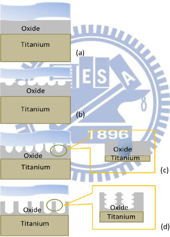
Figure 2.7 Schematic diagrams illustrating the formation mechanism of TiO2 nanotubes structures (a) oxide layer
formation, (b) semicircle pores formation on the oxide film, (c) growth of the semicircle pores into
scallop shaped pores, and (d) fully developed nanotube arrays. ... 32 Figure 2.8 Schematics of the pH profile developing within the tubes during the anodization process according to
Macak et al. ... 33 Figure 2.9 Schematic diagrams of the oscillation mechanism: formation of tube spatial periodicity and corresponding
current behavior under different conditions: (a) without stirring; (b) at medium stirring rate; (c) at high stirring rate or with periodic modulated voltage. ... 34
Figure 2.10 FE-SEM images of nanotube arrays anodized under 10V at: (a) 5°C with an average wall thickness of 34 nm, and (b) 50°C with an average wall thickness of 9 nm. The pore size is 22 nm for all samples.
... 35
Figure 2.11 Schematic illustration of TiO2 nanowires/ nanobelts standing on TiO2 (Right), nanotube arrays section drawing of given regions (Middle), and FE-SEM images corresponding to section drawings (Right) ... 36
Figure 2.12 Different TiO2 crystal structures: (a)rutile, (b)anatase, and (c) brookite. Images courtesy of Joseph R. Smith, University of Colorado ... 37
Figure 3.1 Schematic diagram of anodization reaction system. ... 46
Figure 3.2 The DSSC fabrication process. ... 47
Figure 3.3 Diagram of Experimental Design and Flow: sample preparation and characterization ... 48
Figure 4.1 SEM images of TiO2 films prepared by various anodizing voltage: (a)30 V, (b) 40 V, and (c) 50 V for 0.5h. ... 59
Figure 4.2 Schematic diagrams along with their corresponding surface morphology SEM images for four key stages in the TNWs/TNAs formation mechanism: (a) thinning the tube wall thickness with high roughness near the TNAs mouths, (b) forming strings of through holes in the top section of TNAs, (c) splitting into nanowires, and (d) collapsing and further thinning of nanowires ... 60
Figure 4.3 The condition of required anodizing voltage and processing time (shaded zone) for forming forming TNWs/TNAs (white zone) and the excluded shaded zone for forming TNAs only. ... 61
Figure 4.4 (1) Surface and (2) cross-sectional morphology of TNWs/TNAs hybrid structure under anodizing voltage of 40 V and various anodization time: (a) 0.5h, (b) 2h , and (c) 4h. ... 62
Figure 4.5 Surface morphology of TNWs/TNAs hybrid structurenear the tube mouth films prepared at 40 V and under different anodizing time: (a) 2 h, (b) 3 h, (c) 4 h, and (d) 5 h. ... 63
Figure 4.6 Surface morphology from nanobelts to nanowires under 40 V for 4 h: (a) holes on the nanobelt, and (b) nanowires with smaller width. ... 64
Figure 4.7 The wall thickness and diameter of nanotubes in the top section of TNAs with and without mechanical stirring: from 10 V to 60 V and a processing time of 0.5h. ... 65
Figure 4.8 SEM images of the TiO2 films prepared by anodic oxidation for 30 V under different conditions: (a)
mechanical stirring for 4 h, (b) mechanical stirring for 6 h, (c) non-stirring for 4 h, and (d) non-stirring for 6 h. ... 66
Figure 4.9 Schematic representations of relevant processes in TiO2 nanotube formation and dissolution. [104] ... 67
Figure 4.10 Schematic diagrams along with the consideration of the transport processes of ionic species (F-, O2+, and H+ ) : (a) non-stirring, and (b) stirring. ... 68 Figure 4.11 SEM images of TiO2 films used in DSSCs: (a1) 40 V/TNWs/TNAs, (b1) 30V TNA, (c1)
30V/TNWs/TNAs, and (d1) 40V/TNA ... 69 Figure 4.12 SEM images of thickness TiO2 films used in DSSCs: (a2) 40V/TNWs/TNAs, (b2) 30V TNAs, (c2)
30V/TNWs/TNAs, and (d2) 40V/TNAs ... 70 Figure 4.13 UV-Visible spectra of the desorbed dye from the solutions of various TNAs, TNA/TNWs, and TiO2
Chapter 1 Introduction
After industrial revolution, energy consumption increased drastically. Since 19th century, new kind of energy, especially fossil fuel, was developed one after another. However, the reserves of petroleum are limited and going to be exhausted by this century. Also, the widespread usage of fossil fuel has caused serious environmental pollution and ecological damage. United Nation Framework Convention on Climate Change (UNFCCC) and Kyoto Protocol clearly emphasize the importance of renewable energy development.
Renewable energy including waterpower, wind power, solar, biologic energy, and terrestrial heat, can transfer into electric power, heat, chemical power and fuel. In all kinds of energy, solar energy is almost inexhaustible and without environment pollution. The supply of energy from the Sun to the Earth is gigantic: 3×1024 joules a year, or about 10,000 times more than the global population currently consumes, which means converting 0.1% of the Earth’s surface using solar cells with an efficiency of 10% would theoretically satisfy our present needs. [1]
Nevertheless, the solar energy from the sun cannot be use efficiently. Part of the sun power would be absorbed by the Earth’s atmosphere or reflected to space. Even though the sun energy is hard to be used efficiently, solar power still offers a realistic solution to energy problems. This is the reason why solar cells have attracted extensive attention and fast development. . Solar can be transformed to electricity, fuels, and heat passes without noise. And it produces no air pollution. Massive solar power conversion would ensure abundant energy and safe clear environment for future generations. In all kinds of solar cells, silicon (Si) based solar cells are more mature to become the main products on the market. However, the cost of silicon base solar cells is relatively high.
Therefore, it is important to develop solar cells with low cost and high conversion efficiency for popular use.
B. O’Regan and M. Grätzel in 1991 developed a new kind of solar cell, dye-sensitized solar cell, which has relatively high conversion efficiency, simple fabrication process, low production cost, and transparency [ 2 ]. In 2011, great conversion efficiency 12.3 % has been reported for DSSC based on nanocrystalline TiO2 film, ruthenium sensitized dye, triiodide/iodide redox couple in organic solvent as the electrolyte and platinum coated counter electrode. [3]
The performance and efficiency of the DSSC depend on many factors such as the platinum layer of the counter electrode, the TiO2 layer surface morphology and the
structure, dye molecules, the status and component of the electrolyte. In the TiO2 layer,
mesoporous nanocrystalline TiO2 films provide large surface area for dye adsorption,
electrical connection with the redox electrolyte, electron diffusion and transportation. However, the efficiency was limited at interface traps and electrons recombination. In recent years, various forms of TiO2 nanostructures such as nanorods, nanotubes, and
nanowires have attracted significant research interests to enhance the electron transportation [4,5]. Several studies reported that one dimensional TiO2 nanostructure
could improve the charge-collection efficiency by promoting a better transport route than nanoparticles. [ 6 , 7 , 8 ] and resulted in lowering electron-hole recombination probability [9].
TiO2 nanotube arrays (TNAs) grown by electrochemical anodization method was
first reported by Zwilling et al. [69] with a length up to 500 nm (10:1 aspect ratio) using HF-based aqueous electrolyte. Several neutral electrolytes such as ethylene glycol (EG) or ammonium fluoride (NH4F), have been employed to prepare anodized TiO2
self-organized TiO2 nanotubes have been produced using EG solution [73]. However,
most of studies have been dedicated to one specific type of 1D TiO2 structures such as
nanotubes, nanorods, or nanowires, with less research on 1D TiO2 hybrid structures.
Lim and Choi[10] demonstrated the TiO2 nanowires directly connected TiO2 nanotubes
arrays structure (designated as TNWs/TNAs) using EG and NH4F under mechanical
stirring and proposed a bamboo-splitting model. Recently, Hsu et al. [100] fabricated TNWs/TNAs hybrid structure by a one-step anodization method without mechanical stirring, for photocatalysis application. Yet, little work has been reported on the applications of TNWs/TNAs and TNAs for DSSC, especially as a flexible device. Also, the details of the formation mechanism for TNWs/TNAs under stirring still needs to be clarified.
This study investigates a one-step method for the fabrication of a TNWs-covered TNAs (TNWs/TNAs) hybrid structure, using a mixture of EG and water containing NH4F electrolyte with and without mechanical stirring. The morphology of the
TNWs/TNAs structure was then examined by changing the anodizing voltage and processing time, to elucidate the detailed formation mechanism of TNWs/TNAs. The DSSC performance of TNWs/TNAs and TNAs structures was investigated and compared with the film made of TiO2 nanoparticles.
1.2 Overview
This thesis is organized in five Chapters. In Chapter 1, the advantages and working principle of dye-sensitized solar cells (DSSCs) are introduced. One-dimensional TiO2
structures including TiO2 nanotubes (TNAs) and TiO2 nanowires/TNAs hybrid structure
for photocatalysis and DSSC applications have been used for photocatalysis application. In this study, the preparation of TNWs/TNAs hybrid structures was examined at various applied voltage and time under stirring, compared those prepared without mechanical
stirring of solution. Also, we plan to further explore the TNWs/TNAs hybrid structure for DSSCs application.
Chapter 2 reviews the literatures of the anodizing oxidation method for preparing TNAs and TNWs/TNAs hybrid structure. Chapter 3 covers the experimental details of preparing TNWs/TNAs hybrid structure and the electric measurement of DSSC performance. In Chapter 4, we focus on the results and discussion on the fabrication and formation mechanism of TNWs/TNA hybrid structure using mechanical stirring of solution. In addition, the performance of DSSC based on TNWs/TNA hybrid structure was illustrated and compared to DSSCs based on TiO2 particles, TNAs, and
TNWs/TNAs. At last, summarize the key findings and contribution of this work as well as the future work in Chapter 5.
Chapter 2 Literature Review
2.1 Dye-sensitized Solar Cell
In 1991 Brian O’Regan and Michael Grätzel proposed a high efficiency photovoltaic cell with TiO2-based film as semiconductor electrode, ruthenium (Ru)
organometallic compound as light sensitizer, and suitable redox couple solution as electrolyte [4]. This solar cell called “dye-sensitized solar cell” which had 7.1% conversion efficiency under sun illumination. The cell conversion efficiency reached a breakthrough, 10% in 1999 [12]. The best record (2011) of DSSC conversion efficiency is higher than 12.3%, using porphyrin as a sensitized dye, and Cobalt (II/III) as redox electrolyte. [13]
2.1.1 The Structure and Working Principle of DSSC [1]
The structure of DSSC is a sandwich structure consisting of TCO glass, dye sensitized TiO2 layer, electrolyte, and platinum coated counter electrode.
Figure 2.1 demonstrates the schematic structure of DSSC. The photoanode, which is made of TiO2 dye-sensitized semiconductor, receives electrons from the photo-excited
dye which is oxidized. The oxidized dye molecules then turn to oxidize the mediator, the redox species in the electrolyte and regenerate dye. The mediator is regenerated by the redaction at the cathode by the electrons circulated through the external.
1. Photoexcitation on dye molecules to induce charge separation:
Dye + hv → Dye* (2-1)
2. Charge (electron) injects into conduction band of TiO2:
Dye* → Dye+ + e-TiO2 (2-2)
3. Charge passes through outer circuit via electronic load:
e-TiO2 e
-
counter
(2-3)
2Dye+ + 3I- → 2Dye + I3
-
(2-4)
5. Redox couple reduces on counter electrode by the charge comes from outlet circuit:
I3
-
+ 2e-counter → 3I
-
(2-5)
The Total Reaction:
e-(counter) + hv → e-(TiO2 electrode) (2-6)
The TiO2 electrode does not work as the main light absorption character, but used a
carrier transport host material inside DSSC systems. The synthesized organic dye attached to TiO2 absorbs almost the visible light and made carrier injected from excited
dye molecules then quickly transport to the current collector and then the outer circuit. It avoids the direct charge recombination, which is the energy-favored process after charge separation. The electrons and holes run different routes back to their ground state; this important property contributes to the unusual charge separation efficiency inside DSSC systems.
The root-causes for low DSSC conversion efficiency include, for example, electron/hole recombination inside DSSC, resistance of the materials and impedance at each material interface. The main recombination reactions are at TiO2/dye interface and
TiO2/electrolyte interface, which might cause photocurrent loss.
Equation of recombination at TiO2/dye interface:
Dye+ + e-TiO2 → Dye (2-7)
Equation of recombination at TiO2/electrolyte interface:
3I- + 2e-TiO2 → I3
-
(2-8)
The resistance is decided when the material was chosen, but the impedance at each interface can be reduced by surface modification and post-treatment to improve the connection of each materials.
2.1.2 Operation Principles of Dye-sensitized Solar Cells
1. Open Current Voltage (VOC) Characteristics
When photovoltaic devices are under illumination, the open circuit voltage can be calculated from the diode equation. [14]
(2-9)
Where n is the ideality factor whose value is between 1and 2 for DSSC, and i0 is the
reverse saturation current, which can be measured in reasonably large reverse voltage. There are two main characteristic quantities, the open circuit voltage (VOC), which
represents the voltage produce in the absence of any current, and short circuit current ( ISC), which stands for the current with no voltage across the cell.
The open circuit voltage is determined by the energy difference between the Fermi level of the semiconductor under illumination and the Nernst potential of the redox couple in the electrolyte. However, the experimentally observed open circuit voltage for various sensitizers is smaller than the difference between the conduction band edge and the redox couple. This is generally due to the competition between electron transfer and charge recombination. [15]
When photovoltaic devices are in dark, they should obey the ideal diode equation:
(2-10)
This indicates that a positive applied voltage can make current flow easy.
2. Incident Photons to Current Conversion Efficiency (IPCE)
IPCE is an important parameter when determining the performance of a photovoltaic device. IPCE is defined as the number of electrons flowing through the external circuit over the number of photons incident on the cell surface at a particular
wavelength, which means IPCE the ratio of the observed photocurrent over the incident photon flux.
3. Cell Efficiency (η)
We called VOC as the maximum voltage at photovoltaic device, and ISC as the
maximum short circuit current under illumination. The IV-curve yielding the maximum power is called PMAX. In addition, another important parameter of cell performance is
the Fill Factor (FF), which is defined as follows:
(2-11)
FF is an efficiency factor, used for checking whether the PMAX is ideally equal to
VOC × ISC or not, because there are many types of impedances, including the contact
resistance, electrolyte resistance, and charge transfer resistance, etc. inside the cell, may cause potential drop.
The overall energy conversion efficiency (η) is defined to be the maximum power generated by DSSC under illumination:
(2-12)
Equation (2-10) indicates high open circuit voltage and short circuit current are necessary for high overall efficiency, but the conversion efficiency will still be low without high fill factor (FF).
2.2 Components of DSSCs
2.2.1 Substrate
The most commonly used substrates for DSSC are transparent conducting oxide (TOC) coated glass substrates. For meeting the trend of consumer electronic devices, a new focus of DSSC technology is directed to the realization of light weight film-type cells. Electrochemical anodic oxidization of titanium metal foil could fabricate highly
ordered TiO2 array. Therefore, TCO coated solid glass substrate is replaced with a TiO2
nanotube arrays and TiO2 nanowires/TNA hybrid on a Ti foil in this study.
2.2.2 Nanocrystalline Photo-anode
Titanium dioxide is a fundamental semiconductor for DSSC because of its non-toxic properties, easy produce process, high stability and low cost. Energy conversion in a DSSC is based on the injection of an electron from a photo-excited state of the sensitizer dye into the conduction band of semiconductor.
For nanoparticle TiO2 film, there are two methods to prepare photoanode. One is
the “sol-gel method” [16,17], by which TiO2 is prepared from hydrolysis of Ti-alkoxides
and addition of a binder. Narrow particle size distribution and fine-ordered crystal structure can be obtained by carefully controlling every preparing step. However, this method is limited to small scale for laboratory only, although these properties are desired in standard electrode.
Nanoparticle efficiency was limited in the random walking of electron transport and recombination. To improve the efficiency of charge collection and reduce the recombination, different TiO2 morphologies, such as vertically TiO2 nanotube arrays,
nanorods, and nanowires, have been investigated. Recently, TiO2 nanotubes were
applied in solar cells. [1] The conversion efficiency was reported to increase from 1.6% to 1.9% under various tube length and morphology. [1]
There are many methods for preparing nanostructured TiO2 electrodes, including
electrodeposition [18,19,20], evaporation[21], sputter deposition [22,23,24,25,26], and chemical vapor deposition [27,28]. The highly-ordered TiO2 nanotube arrays [29] and
mixture of TiO2 nanowires and nanoparticles [ 30 ] are typically used as the
photo-electrode.
which is the result of competition between field-assisted anodic oxidation and electrochemical etching. “Electrochemical anodization method” which Zwilling and co-worker published the first report on anodized TiO2 nanotube in 1999. [11]The typical
porous structure observed only in sufficient HF was added to the electrolyte mixture called the first generation. In subsequent work, the smooth and long tube has been controlled in various electrolytes due to the different ion diffusion and the amount of water. [31,32]
2.2.3 The Sensitizer: Organic dye
As mentioned before, the organic dye becomes a sensitizer which absorbs most of the incident light and increases the cell efficiency. Organic dye used in photoelectron chemical cells should meet the follow needs:
1. Absorption: With good absorption in visible light region up to wavelength 920nm, almost the incident light from sun.
2. Energetic: With sufficient electrons on excited state providing the driving force to make electrons inject to conduction band of TiO2 thin film. Organic dye should also
have relative low ground state for reduction by the redox couple in electrolyte.
3. Kinetics: The rate of electron injection should be high, and the lifetime of excited electrons should be long enough.
4. Stability: The organic dye can be operated under normal environment for more than 108 times of the redox cycle reaction and can be operated for more than 20 years. 5. Interfacial properties: It can attach on TiO2 surface and cannot be easily desorbed
A breakthrough of organic sensitized dye is accomplished by Grätzel’s group at EPFL in Switzerland by using metallo-organic ruthenium complex as the “dye” along with nanostructured TiO2 electrode.[4] The dye have the general structure ML2(X)2,
where L stands for 2,2’-bipyridyl-4,4’-dicarboxylic acid, M for ruthenium or osmium and X for halide, cyanide, thiocyanate. The cis-RuL2 (NSC)2, also called N3 dye has
shown impressive performance. Figure 2.2 compares the spectral response of the photocurrent observed with two sensitizers. The incident photo to current conversion efficiency (IPCE) of DSSC is plotted as a function of excitation wavelength. Both chromophores show high IPCE values in the visible range. However, the response of the black dye extends 100nm further into the IR than of N3. The photocurrent onset is close
to 920 nm, i.e. near the optimal threshold for single junction converters. Recently, there is a credible challenger identified to the “black dye” (tri(isothiocyanate)-2,2’,2”- terpyridyl-4,4’4” -tricarboxylate)Ru (Ⅱ).
Lately several studies showed up by modifying the function groups to improve excitation lifetime and increase the open circuit voltage of the cell which are called N719, N749 (black dye)…etc. (see Figure 2.3).
Recent work has focused on the molecular engineering of suitable ruthenium compounds, which are known for their excellent stability. Cis-Di-(thiocyanato)bis(2,2’-bipyridyl-4,4’-dicarboxylate)ruthenium(Ⅱ), coded as N3 or N719 dye depending on whether it contains four or two protons. N719 dye was found to be an outstanding solar light absorber and charge-transfer sensitizer. Figure 2.4 shows the structures of three ruthenium complexes with different colors that have been widely employed as sensitizers for the DSSC. This feature can be applied to design multicolor DSSC in art and architecture.
which the sintered TiO2 electrode is immersed into a dye solution, usually 2×10⁻⁴M in
solvent traditionally. The dye adsorption should be done immediately after high temperature sintering process for TiO2 electrode for not letting water content in the
pores of electrode react with the excited dye molecules to reduce any impact on the long-term stability. In practice, we keep the photoelectrode in anhydrous condition before and after dye adsorption. The overall dye adsorption process should be stored in a moisture-free environment.
2.2-4 Electrolyte
Electrolyte systems consist of redox couple and solvent, which works as reducing agentproviding electrons to redox the oxidized dye molecules at photoelectrode and as oxidant receiving from counter electrode.
Redox Couples
Requirements and properties of redox couple in electrolyte should be defined: 1. Redox potential
The redox couple reversible potential has to be equal to the negative of dye reversible potential. The more negative the potential, the large the thermodynamic driving force for the dye regeneration. However the potential request should make the balance between the driving and the open circuit potential hence the cell performance in order to avoid unnecessary loss of usable energy.
2. High solubility
To make sure sufficient supply of the redox mediator and to minimize the possibility of diffusion-limited situations, an adequate concentration of redox couple is needed. Because diffusion-limited would result in an undesirable lifetime of the oxidized dye and consequently would increase the possibility of dye decomposition. Concentration are commonly used at 0.1-0.5M
A high diffusion coefficient is needed because the mass transport of the redox couple in a solar cell (through solution and TiO2 network) occurs solely by
diffusion.
4. No significant spectral characteristics in the visible region. In order to prevent the situation of less light being available for the light-to-electricity conversion and thus low energy conversion, the redox couples should not able to have absorbance in the visible light region.
5. High stability of both the reduced and oxidized forms of couple
For efficient redox “shuttling” in solar cells, both the oxidized and reduced forms of the couple need to be present in solution and both forms must have high stability. In the case of iodide/triiodide system, the reduce form is in excess. [33,34] 6. Highly reversible couple
The oxidation of the reduce form and reduction of the oxidized form of the redox couple must be electrochemically and chemically reversible to ensure the fast electron transfer and avoid unwanted side reactions.
7. Chemically inert system
The components of the redox couple system must be chemically inert to avoid the side reaction, e.g., no chemical reactivity with TiO2, no surface activity, etc.
Based on the requirements listed above, many redox couples have been tested for DSSC systems. Now the I-/I3
-
redox couple still remains the best choice because of its kinetics and suitable redox potential for TiO2 electrode. In practical use, the
redox couple is prepared by dissolving I2 and some iodine salt such as KI, LiI, alkyl
methylmidazolium iodide, etc. to form I-/I3
-
couple. The triiodide would form instantaneously when iodide is added into iodide via this equation:
I-+ I2 → I3
-
Ionic liquid utilizing iodide as anion like DMPII (diemethyl-propyldazium iodide) has also been introduced to be iodide source in DSSC systems. It is believed that those “liquid-like” salts have higher dissociation rate than tradition iodide salt.
Solvents used for electrolyte
Some criteria are made for a suitable solvent for liquid-type electrolytes as below: 1. The solvents must be liquid and have low volatility at the operation temperature
(usually 40-80℃) to avoid freezing or expansion of the electrolyte which would damage the whole cells.
2. They have low viscosity for rapid diffusion of carriers.
3. The chosen redox couple should have high dielectric constant to promote dissolution in solvent.
4. The solvent should not make desorption or dissolution of sensitized dye. 5. The solvent should not decompose under illumination or after long time use.
6. The solvent should better be low cost for large scale production, and have low toxicity.
Typical liquid solvents are acetonitrile (ACN) [ 35 ], methoxyactonitrile, methoxypropionitrile (MPN), ethylene carbonate (EC) [36], propylene carbonate [37], etc. and their mixture [38,39,40,41]. ACN has performed the best among these solvents, but it is still not well-received due to two reasons: (1) highly volatile with low boiling point (82℃) and (2) it is carcinogenic.
There are also new conceptions for the electrolyte of DSSC: Quasi-solid state polymer electrolyte, using ionic liquid as solvent for electrolytes containing an I-/I3
-
redox couple. [42] The request for long-operation stability of DSSC is a driving force of to substitute liquid electrolyte by solid or quasi-solid state electrolyte. [43,44,45,46,47] However, the mass transport of the triiodide ion has been considered as a limiting factor
for ionic liquids due to their low diffusion coefficient and lower concentration in these electrolytes versus iodide. A high concentration of redox couple is needed to achieve a domination of the exchange-reaction based fast charge transport process between I- and I3
-
in viscous electrolytes. On the other hand, the absorption in visible light by I- competes with the absorption of the dye and high concentration of I- promotes the back electron transfer from conduction band of the photoanode to the triiodide [48].
2.2.5 Counter electrode
The reaction on counter electrode is a triiodide reduction:
I3
-
+ 2e- → I- (2-14)
This reaction plays an important role in the overall DSSC system because it is responsible for the regeneration of oxidized dye molecules. The conversion efficiency of DSSC might be lowered if the speed of dye regeneration is lower than the dye oxidization by photo injection.
Since the ITO or FTO shows slow kinetics of triiodide reduction in organic solvents [49,50], catalytic material is coated in order to accelerate the reduction reaction. Platinum (Pt) has been almost exclusively as the catalytic material. However, different methods preparing thin Pt film lead to different efficiency and cost. Fang et al. used sputtered Pt layer and they found out that the sputtered Pt layers on different type of substrates (steel sheet, nickel sheet, polyester film, and conducting plastic film) have slightly different cell efficiencies in comparison with that based on a conducting glass. [51] In recent reports, Kim et al. [52] have demonstrated the preparation of a new counter electrode consisting of Pt nanosized phase in NiO or TiO2 porous phase using a
RF co-sputtering system. They indicated that by applying Pt in a metal oxide biphase electrode, the short circuit current density and cell efficiency were increased due to the increased active surface area of the nanosized Pt.
cost and the environment request of ultra-high vacuum. N. Papageorgiou [53] developed a method called “thermal cluster platinum catalyst” (TCP). Counter electrode made by this method has low Pt loading (around 2-10g/cm3), superior kinetic performance, and mechanical stability comparing with other deposition methods like sputtering, spin coating, thermal [5, 54], and electrochemical deposition.
Wei et al. [55,56] developed a simple technique called “two-step dip coating” for preparing a Pt nanoclusters counter electrode for DSSC system. With an appropriate surface conditioner, the adhesion of PVP-capped Pt nanoclusters on ITO glass becomes satisfactory. Electrodes employing this method exhibit not only ultralow Pt usage but also good catalytic performance.
Other materials can be used as the counter electrode, such as conducting polymer [57,58], nanocarbon [59], carbon black [60,61] and carbon nanotubes [62]. Some even use polymer-catalyst composites [63,64,65]. These new material used as counter electrode usually requires porous film on the substrate to obtain acceptable catalytic reduction efficiency.
2.2.6 Sealant and Spacer
Sealing is a very important process in DSSC system to avoid the humid environment and to prevent the decomposition of dye molecules. The thickness of spacer is also having dilemma between making lower IR drop and the risk of short circuit.
Surlyn® (SX1170-60), a thermoplastic resin which has good toughness, becomes a good sealant used in DSSC. It is inert to electrolyte and shows great tightness. However, there are still other types of resin which also used in DSSC system.
2.2.7 Post-treatment/Pretreatments/Underlayer
improve the performance of DSSC based on the fact that an extra layer of TiO2 is grown
onto the TiO2 nanotube arrays and hybrid nanowire structure constituting the film.
There are many hypotheses concerning the following aspects: (1) Surface area[67]
(2) Electron transport[64] (3) TiO2 purity[68]
(4) Dye anchoring[69]
These post-treatments have been carried out by TiCl3 electrodeposition,
Ti-isopropoxide and, the best, titanium tetrachloride (TiCl4) post-treatment [70]. The
effect of these post-treatment is believed to increase the dye loading making more efficient photon-current conversion which affect the short circuit current density (JSC),
and the current conversion efficiency (IPCE). It is also important to note that the TiCl4
treatment would not be beneficial if a given TiO2 nanoparticle film is already at the
correct potential to reach the maximum efficiency of the electron injection, which depends on the history and source of TiO2 to be made. In addition, another report
indicates that the TiCl4 pretreatment to ITO or FTO can certainly enhances the
suppression of dark current leading an increase in VOC and enlarge the surface area of
the mesoscopic film leading the improvement of JSC [71].
Xia et al. reported a new FTO/ TiOX/ mesoscopic TiO2 electrode was used as the
blocking layer of DSSC [72]. According to their study, the blocking layer reduced the electron loss at the FTO/ mesoscopic TiO2 and FTO/electrolyte interface by a TiO2
compact layer between the FTO and mesoscopic TiO2 layer which made by RF
sputtering system. This is also another discovery finding out a layer made by TiO2 can
2.3 Anodic oxidization technique
2.3.1 The development of anodized TiO
2nanotubes
First generation of TiO2 nanotube
In 1999, Zwilling and co-workers anodizes Ti and Ti-6Al-4V (TA6V) alloy in an electrolyte containing 0.5 M chromic acid and 0.095 M HF [73], while the first report on anodized TiO2 nanotubes (called first generation). The nanoporous structure observed
only under a sufficiency HF was added to the electrolyte mixture, as pure chromic acid (CA) was leading to the formation of a thin but stable oxide layer with no apparent pore structure. Otherwise, the length of this kind method could enhance for a long processing time. TiO2 nanotubes reach a steady state length when anodized. After typically 10 to 20
minutes of anodization, the etching rate equals the dissolution rate and it causes the length of nanotube stop increasing with additional anodizing time.
Second generation of TiO2 nanotubes
Grimes and co-workers [74]overcome the limitation described before since they knew other fluorine salts (as fluorine ion source besides HF) and combined buffers, bases and milder acids to adjust the pH and fluorine ion content. Salts like KF, NH4F, or
NaF totally dissociate in aqueous solution and then hydrolyze with water to form HF [75]. Moreover, HF is a relatively mild acid in acidic solution (pH<3.45) more than 50% of the fluorine exist in the form of HF. As a result pH and fluorine ion concentration are closely related (and solutions with KF, NaF, and NH4F and no
additional acid are basic.) The experiments found that they could grow nanotubes up to 4.4 µm (Figure 2.5) using a solution of 0.1 M KF as fluorine source, 1 M H2SO4 as acid,
0.2 M citric acid presumably serving as buffer and NaOH as base to be added until the desired pH of 4.5 was obtained [72]. Later in 2005, Grimes and co-workers reported even longer nanotubes of up to 6 µm, over 17 to 20 h of anodization using the
electrolyte as before [76].
Third generation of TiO2 nanotubes
The third generation of nanotubes refer to smooth tubes (no ripples along the wall),
prepared by using organic electrolytes (some almost water-free) to minimize the dissolution rate of formed oxides.
As illustrated in Figure 2.6 [77], it can be observed that tubes obtained in water are much rougher and irregular than the other. The reason was to use a viscous electrolyte, where ion diffusion is slower than in water. Meanwhile, the pH gradient between the bottom and top of the tubes increased. This led to the formation of TiO2 nanotubes up to
7 µm thick (compared with the first generation). It implied that smoothness and regular morphology of the tube walls to the lower diffusion coefficient of the electrolyte which suppresses pH burst at the pore bottom which occur when working in aqueous media. TiO2 nanotube arrays with lengths of up to 1000 µm were achieved using a non-aqueous,
polar organic electrolyte such as formamide, dimethyl sulfoxide, ethylene glycol or diethylene glycol [78,79,80].
In 2007, Grimes and co-workers published the synthesis of 0.36 mm long nanotube [76], practically demonstrating that the nanotube lengths was only limited by the initial titanium foil thickness. The following section will discuss the fundamental aspects and chemistry of the growth of TiO2 by anodization.
2.3.2 The growth of TiO2 nanotube: fundamental aspects
The formation mechanism of TNAs nanostructure is similar to anodic aluminum oxide (AAO), which is the result of competition between field-assisted anodic oxidation, defined as the formation of the anodic layer under a applied electric field by Eq.(2-15)-(2-17) and chemical/field assisted dissolution of the forming oxide by Eq. (2-18), which can be regarded as dissolution promoted by the presence of fluoride ions
(chemical dissolution) and by the electric field weakening the bond between Ti and O (field assisted dissolution)[81]:
Electrochemical reactions of anodic titanium oxide At Ti / Ti oxide interface:
Ti→Ti2+
+2e- (2-15) 2H2O→2O-2+4H+ (2-16)
Ti2+ +2O2-→TiO2+2e- (2-17)
At Ti/Ti oxide interface:
TiO2+6HF→TiF62-+2H2O+2H+ (2-18)
Meanwhile, the formation mechanism of the TiO2 nanotubes at various stages is
schematically illustrated by Figures 2.7(a)-(d). Initially, field-enhanced oxidation occurs at the Ti/Ti oxide interface by Eq. (2-15)-(2-17) when oxygen ions diffusion to the Ti layer as shown in Figs. 2.7(a). At the same time, competing field-enhanced oxide dissolution occurs at Ti/solution interface illustrated by Fig. 2.7(b). Specifically, fluoride-containing electrolyte reacts with TiO2 to form TiF62
-as described by Eq. (2-18). Moreover, small pores are generated and spread uniformly over the surface of the film under an electric field. When the pore to pore distance achieves a suitable value at which the electric field of each pore would not affect each other, the distribution of electric-field strength would change.
As a consequence, under increased in local field strength at the bottom of the pore in conjunction with low dissolution rate at the sidewall, highly-order pore structures were formed as shown in Figure 2.7(c). Finally, in the growth stage, fully developed TiO2
nanotube arrays are shown in Figure 2.7(d). Field- enhanced dissolution developed the depth of the pore to tube. Therefore, the steady-state nanotubes morphology was created.
2.3.3 Key parameters for controlling the growth of the nanotubes
Summarizing anodic oxidation technique, the key parameters to be considered when anodized TiO2 nanotube and hybrid structures are the following:
Electrolyte
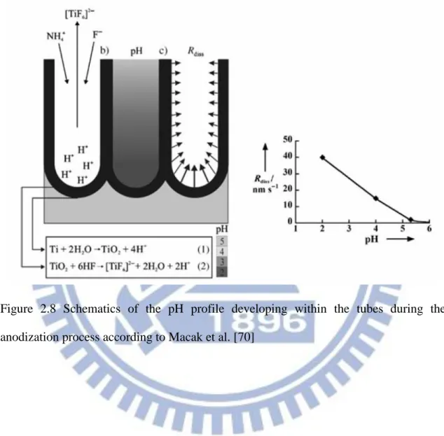
The electrolyte plays a crucial role in the growth of anodized TiO2 nanotubes, as
previously discussed. The main distinction is between aqueous and organic-based, where the water content is an important rule to limit dissolution of the oxide. Moreover, the pH of the solution is also important, considering the higher dissolution rate of the oxide in an acid environment. As shown schematically in Figure 2.8. While the pore bottom is at a low pH, the pore mouth (top of nanotubes) remains under a protective environment (higher pH) by using chemical buffer species [NH4F/
(NH4)2SO4]. The rapid rate of the TiO2 dissolutions in the first generation of nanotube
was reduced by replacing the HF acid [70] with less aggressive solutions containing fluoride salts, and raising the maximum thickness up to 2-3µm. [75] This is one of the reasons why dissolution was reduced of the TiO2. If the anodic oxide is at its lowest
when using fluoride salts (some of them have basic hydrolysis) instead of hydrofluoric acid.
Mechanical stirring system
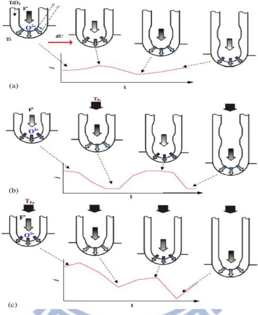
The mechanical stirring was sometimes used to accelerate the reaction rate for nanotube growth. In addition, mechanical stirring also affect the inner tube morphology of TNAs. Figure 2.9 shows the schematic diagram of the formation of the tube spatial periodicity under different conditions: (a) without stirring; (b) at medium stirring rate; (c) at high stirring rate [82]. The smoothing effect of the tube inner surface and the acceleration of the growth are due to the redistribution of the F- anions in the nanotubes. Based on the experimental results, the mechanism has been discussed with the
Under this interpretation, the current oscillation and the morphology change in the pore are attributed to the redistribution of the ionic species by the fluctuation in the tube layer when there is no stirring. They can be significantly influenced by the convection above the tube layer and the slow transport process in the tubes with the existence of mechanical stirring.
Temperature
The temperature of the electrolyte affects the chemical dissolution and electrochemical dissolution and electrochemical etching rate in the growth of the nanotube arrays via anodic oxidation of titanium. For example, Grimes reported nanotube arrays were grown with a constant 10 V anode potential in an electrolyte of acetic acid plus 0.5 % HF mixed 1:7 ratio and kept at each of different electrolyte bath temperature: 5°C, 25°C, 35°C, and 50°C. Table 2.1 shows the variation in 10 V wall thickness and tube length as a function of anodizing temperature .Figure 2.10 shows the FE-SEM images of morphology of TiO2 nanotubes fabricated by anodizing at 10 V at (a)
5°C and (b) 50°C. The pore diameter is essential the same (22 nm) for the 10 V anodized TiO2 nanotube arrays at these different temperatures.
Results show that with decreasing anodizing bath temperature the wall thickness increases from 9 nm at 50°C to 34 nm at 5°C, confirming the trend of the increasing nanotube wall thickness with decreasing temperature.[83]
2.3.4 Application on DSSCs of TiO2 nanotubes arrays
Recently, research has been directed toward synthesizing structures with a high degree of order than the random assembly of nanoparticles. A desirable morphology of the films would have the mesoporous channels or nanorods aligned parallel to each other and vertically with respect to the glass substrate. This would facilitate charge diffusion in the pores and the mesoporous films, giving easier access to the film surface, avoiding grain boundaries and allowing the junction to be formed under better control.
One approach to fabricate such oxide structures is based on anodized TiO2 nanotubes by
Frank and co-workers [84]. They reported that the nanotubes and the nanoparticles in conventional DSSCs have similar transport properties (the electron has to diffuse though the oxide and reach the electrode to feed the circuit), however lower recombination occurs in the nanotubes because of a higher charge collection efficiency. In addition, the nanotubes harvest the light more efficiently than conventional DSSCs, because of stronger light scattering effecting. However, their use in DSSCs still far from optimized.
2.3.5 Challenge of TiO2 nanotubes arrays on DSSCs
From the literature, it has known crystalline nanotube or nanowire based on TiO2,
in contrast with the random transport path in nanoparticle, have been investigated to improve electron collection. Then, there are challenges existing and need to overcome. One of challenges is that 1-D nanostructures have a lower internal surface area than mesoporous films. In DSSC application, the reported efficiency of TiO2 nanotube based
DSSC is generally much lower than DSSCs based on nanoparticles and amounted to 0.61%-2.9% [85,86,73,87]. The possible reason is that the internal surface area of nanotube based photoanode is much smaller than that of nanoparticles due to a lower dye loading and sunlight adsorption.
2.3.6 TiO2 hybrid structure (TNWs/TNAs)
There are various methods fabricating TiO2 which can be organized according the
templates used during the experiment. Sol-gel processing which transcription used organo-gelators as templates [88,89], seed growth [90], deposition into a nanoporous alumina templates, and hydrothermal processes [91].
Among them, anodizing oxidation method is better due to the highly order arrays. Anodizing oxidation carries on producing a long TiO2 nanotube arrays in viscous
electrolyte, and the TiO2 nanowires are found [92]. In 2012, Haijun and the coworkers
[93] found the TiO2 nanobelts exist between TiO2 nanowires as shown in Figure 2.11
2.3.7 Anneal treatment for TiO
2material
Titanium dioxide (TiO2) can exist in three distinct crystalline polymorphs: anatase,
rutile, or brookite crystalline phase, respectively shown in Figure 2.12 [94]. From Figure 2.12, all three crystal structures are made up of distorted octahedra, each one representing a TiO6 unit, where each Ti4+ is at the center of the unit and coordinates six
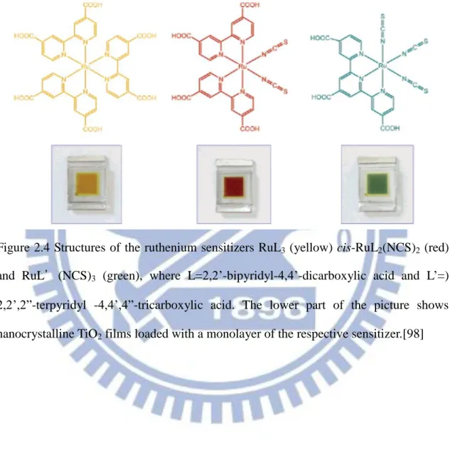
O2- ions. The manner in which the octahedra assemble to form a TiO6 based chain is
different and characteristic of each polymorph. In these three phases, rutile and anatase are the most commonly synthesized phase. Anatase and brookite are metastable phases and convert into rutile at high temperature, usually above 600 °C [95]. Table2.2 lists some of the key properties [90,96] of the three TiO2 polymorphs. Both rutile and
anatase have a tetragonal crystal structure, where brookite has an orthorhombic symmetry. Rutile is the densest phase and has the highest refractive index, while anatase is characterized by the widest band-gap (~3.2 eV) [92]. The properties (density, band-gap, and refractive index) of brookite fall between those of rutile and anatase.
Figure 2.2 (a) Spectral response curves of the photocurrent for the DSSC sensitized by N3 and the black dye. (b) The chemical structures of N3 dye and black dye. [97]
Figure 2.4 Structures of the ruthenium sensitizers RuL3 (yellow) cis-RuL2(NCS)2 (red)
and RuL’(NCS)3 (green), where L=2,2’-bipyridyl-4,4’-dicarboxylic acid and L’=)
2,2’,2”-terpyridyl -4,4’,4”-tricarboxylic acid. The lower part of the picture shows nanocrystalline TiO2 films loaded with a monolayer of the respective sensitizer.[98]
Figure 2.5 Lateral view of the nanotubes formed in 0.1 M KF, and 1 M H2SO4, and 0.2
Figure 2.6 A comparison between SEM cross-sectional images of nanotubes in (a) an aqueous based and (b) organic electrolyte [74]
structures (a) oxide layer formation, (b) semicircle pores formation on the oxide film, (c) growth of the semicircle pores into scallop shaped pores, and (d) fully developed nanotube arrays.
Figure 2.8 Schematics of the pH profile developing within the tubes during the anodization process according to Macak et al. [70]
Figure 2.9 Schematic diagrams of the oscillation mechanism: formation of tube spatial periodicity and corresponding current behavior under different conditions: (a) without stirring; (b) at medium stirring rate; (c) at high stirring rate or with periodic modulated voltage. [80]
Figure 2.10 FE-SEM images of nanotube arrays anodized under 10V at: (a) 5°C with an average wall thickness of 34 nm, and (b) 50°C with an average wall thickness of 9 nm. The pore size is 22 nm for all samples. [81]
Figure 2.11 Schematic illustration of TiO2 nanowires/ nanobelts standing on TiO2
(Right), nanotube arrays section drawing of given regions (Middle), and FE-SEM images corresponding to section drawings (Right) [92]
Figure 2.12 Different TiO2 crystal structures: (a)rutile, (b)anatase, and (c) brookite.
Table 2.1 Average wall-thickness and tube-length of 10V titanium nanotube arrays anodized at different bath temperatures [81].
Anodization temperature(°C) Wall thickness (nm) Tube length (nm)
5°C 34 224
25°C 24 176
35°C 13.5 156
Table 2.2 Different TiO2 polymorphs and some of their physical properties[90,92]
Rutile Anatase Brookite
Crystal System tetragonal tetragonal Orthorhombic
Density (g/cm3)[90,92] 4.13-4.26 3.79-3.84 3.99-4.11
Band-Gap (eV)[92] 3.0 3.2 3.11
Refractive Index[92] 2.72 2.52 2.63
Chapter 3 Experimental Section
3.1 Materials
Materials for fabricating TiO2 nanotube arrays structure (TNAs) and hybrid
structure (TNWs/TNAs)
1. Titanium foils 99.9 % purity, 0.5mm thickness and 0.127μm thickness. Sample size 0.28 cm2
2. NH4F from SHOWA for contributing F-.
3. Ethylene glycol (EG) from SHOWA for a high viscosity electrolyte. The structure is :
Materials for DSSCs
1. Titanium tetrachloride (TiCl4) (from SHOWA) is for post-treatment of TiO2 film
2. Titanium foil 99.9 % purity, 0.5mm thickness and 0.127μm thickness.
3. Ethanol (C2H5OH) (from ECHO) is used as a solvent for dye solution and the
chemical structure is:
4. Surlyn® (SX1170-60) (from SOLARONIX) is used as the spacer and sealing material
Materials for electrolyte
1. Lithium iodide (LiI) from MERCK 2. Iodine (I2) from SHOWA
3. 1-methylbenzimidazole from Alfa Aesar and the chemical structure is:
4. Guanidine thiocyanate from Alfa Aesar and the chemical structure is:
5. 1-Methoxypropionitrile (from Alfa Aesar) is a solvent for the liquid electrolyte and the chemical structure is:
3.2 TiO
2films Preparation
3.2.1 TiO
2nanotube arrays film (TNAs)
Titanium foils (99.9% purity) of 0.5 mm or 0.127 mm thickness with a sample size of 0.28cm2, were used as the substrate for forming TiO2 layer by anodic oxidation. Prior to
anodization, Ti foil was ultrasonically cleaned by distill water, rinsed by acetone, and then dried by a purging N2 gas. The schematic diagram of anodizing reaction system is
illustrated in Figure 3.1.
All anodizing experiments were carried out at room temperature using a two-electrode electrochemical cell consisting of a stainless steel foil (SS304) as the cathode and a Ti foil as the anode, at a constant DC potential. The electrolyte: 0.5 wt% NH4F dissolved in the ethylene glycol (EG) solution with 1 wt.% H2O. Anodizing
conditions are (1) 40 V for 30-40 min and (2) 30 V for 4h under stirring at 300rpm. The working layer of DSSCs in the study was fixed at 12µm, unless stated otherwise.
3.2.2 TiO2 hybrid film (TNWs/TNAs)
A hybrid structure composite of TiO2 nanotube and nanowire were fabricated by
using electrolyte consisting of EG and water (99:1 in wt.%) with 0.5 wt.% NH4F. The
conditions of anodizing voltage and processing time were designed to elucidate the formation mechanism of TNWs/TNAs and also fixed in the same thickness to compare the efficiency performance. The electrolyte: 0.5 wt % NH4F dissolved in the ethylene
glycol (EG) solution with 1 wt.% H2O. Anodizing conditions are (1) 40 V for 2h and (2)
30 V for 8h. The working layer of DSSC was fixed at 12µm. Otherwise, we increase the processing time at anodizing voltage of 40 V from 2 h to 5 h in order to examine the transition from nanobelts to nanowires and thickness reaches 15 µm.
3.2.3 Post-treatment for TiO
2films
TiCl4 treatment
The post-treatment was done by immersing the TiO2 anode into the 0.1 M TiCl4
water solution for 30 min in ice bath to form small TiO2 particles on the wall of TNAs
and TNWs/TNAs for increasing the surface area. This can improve the charge transfer between TiO2 films and dye adsorption.
Annealing for TiO2 films
After TiCl4 treatment, TiO2 anode was sintered at 400℃ for one hour to transform the
TiO2 film into anatase phase. For TNAs and hybrid structures, the thermal annealing
was performed in O2 ambient at 400°C for 1 hour under a heating rate of 2°C/min. A
tungsten wire heater was rolled around the quartz tube to create a homogeneous temperature in the furnace.
3.3 DSSC fabrication
The TiO2 photoanode was immersed in a 3×10⁻⁴M N719 dye ethanol solution at
room temperature for 24 hours for dye adsorption. After sensitized, the TiO2 photoanode
was dipped into ethanol to remove extra dye which did not adsorb on the TiO2 surface.
DSSC was fabricated by sealing the dye-sensitized TiO2 photoanode and Pt-sputtered
counter electrode around 100℃ with a hot-melt sealing foil. The hot-melt sealing foil was also served as a 60 μm spacer. There are two tiny holes on the Pt-sputtered counter electrode for injection of electrolyte.
The electrolyte composition was 0.5M LiI, 0.05M I2, 0.2M 1-methylbenzlmidazole,
and 0.5M guanidine thiocyanate in 1-methoxypropionitrile solvent. The electrolyte was injected into the cell through two tiny holes on the counter electrode. After the extra electrolyte was removed, the two tiny holes were also sealed by the hot melt sealing foil
with a normal glass. Figure 3.2 illustrates the schematic diagram of DSSC fabrication process.
3.4 Characterization techniques
3.4.1 Morphology and microstructure characterization of TiO
2nanostructure
The surface and cross-section morphology of TNAs, TNWs, and TNP were observed by a field emission scanning electron microscope (FESEM) (HITACHI-S2500 JSM-6500F). FESEM is a powerful analytic tool for characterizing the microstructure down to several ten nanometers. The detector gathers secondary electrons signal, and transfers into a SEM photo through an amplifier. In practice, a metal layer (ex. Au, Pt) is coated on the samples to alleviate charging effect. FESEM was operated at an accelerating voltage at 15.0 KV. The thickness of TiO2 films were examined by focus
ion beam microscope (FIBSEM), which was carried out at an accelerating voltage at 5.0 KV.
An X-ray diffractometer (XRD) (Siemens Diffractometer, D5000) with Cu Kα (λ=1.5405Å) radiation was employed to analyze the crystal structures of TNAs and TNWs/TNAs.
3.4.2 Dye adsorption measurement
The surface areas of the TiO2 film were measured by dye (N719, dye, Solaronix)
adsorption, which is a commonly used method in DSSC applications [99]. Specifically, the amount of dye adsorption was determined by desorbing the dye from the TiO2 films
into 5mM NaOH aqueous solution. The quantification was based on the dye’s maximum absorption values at 505 nm in the dye-desorbed NaOH solutions as measured by an UV-visible light spectrometer (Evolution300), using a dye solution of concentration 5×10⁻³ mM as a reference.
![Figure 1.1 The path length, in units of Air Mass, changes with zenith angle. [11]](https://thumb-ap.123doks.com/thumbv2/9libinfo/8060436.162941/17.892.157.781.115.899/figure-path-length-units-mass-changes-zenith-angle.webp)
![Figure 2.1 Schematic of DSSC operation [1]](https://thumb-ap.123doks.com/thumbv2/9libinfo/8060436.162941/38.892.158.731.325.900/figure-schematic-of-dssc-operation.webp)
![Figure 2.3 Chemical structures of N719 dye and N749 (black dye) [39]](https://thumb-ap.123doks.com/thumbv2/9libinfo/8060436.162941/40.892.151.729.345.891/figure-chemical-structures-n-dye-n-black-dye.webp)
![Figure 2.5 Lateral view of the nanotubes formed in 0.1 M KF, and 1 M H 2 SO 4 , and 0.2 M citric acid solution (25 V, 20 h)[72]](https://thumb-ap.123doks.com/thumbv2/9libinfo/8060436.162941/42.892.158.784.234.909/figure-lateral-view-nanotubes-formed-citric-acid-solution.webp)
![Figure 2.6 A comparison between SEM cross-sectional images of nanotubes in (a) an aqueous based and (b) organic electrolyte [74]](https://thumb-ap.123doks.com/thumbv2/9libinfo/8060436.162941/43.892.175.744.236.767/figure-comparison-sectional-images-nanotubes-aqueous-organic-electrolyte.webp)