An Ultra Compact and Broadband 15-75 GHz BPSK
Modulator Using 0.13-µm CMOS Process
Hong-Yeh Chang, Pei-Si Wu, Tian-Wei Huang, Huei Wang, Yung-Chih Tsai
*and Chun-Hung Chen
*Department of Electrical Engineering and Graduate Institute of Communication Engineering,
National Taiwan University, Taipei, 106, Taiwan, R.O.C.
*
Taiwan Semiconductor Manufacturing Company, Hsinchu City, 300, Taiwan, R.O.C.
Abstract — In this paper, an ultra compact and broadband 15-75 GHz BPSK modulator using standard bulk 0.13-µm
CMOS process is described. This modulator was constructed utilizing a new reflection-type topology, with the transmission lines implemented on the thick SiO2 layer as the substrate to
avoid the lossy silicon. The overall chip size, including baseband, LO, and RF probe pads, is only 0.5 × 0.35 mm2. Compared with
the previously reported GaAs modulators, this work demonstrates a more than 80% chip area reduction, and features an amplitude imbalance of within 0.5 dB with a phase imbalance of within 3° between 15 and 75 GHz. Regarding the modulation quality, the measured error vector magnitude (EVM) of the BPSK modulator at 40 GHz is within 3.5 and 7% for a data rate of 1 and 10 Mb/s, respectively. The LO-to-RF isolation is better than 40 dB among all the operation frequency. From continuous-wave (CW) spectrum characterization, the modulation bandwidth of the modulator is wider than 1 GHz.
Index Terms — BPSK, CMOS, millimeter-wave (MMW), MMIC, modulator, and reflection-type.
I. INTRODUCTION
Direct carrier modulators have the advantages of low cost and complexity in modern digital transmitters, especially for MMW applications. Most direct carrier modulators employ double-sideband suppression-carrier amplitude modulator, such as ring mixer, star mixer, and Gilbert-cell mixer, due to their high LO-to-RF isolation and spurious suppression [1]. A direct IQ modulator used passive FET in a ring configuration was reported in [2]. The Gilbert-cell based modulators were widely applied to the communication applications [3]-[6]. These modulators demonstrated good performance, but most of them were operated below 10 GHz.
For the MMW applications, balanced W- and Ka-band reflection-type BPSK modulators using 0.1-µm InP and GaAs HEMT were reported by Lo and et al. [7], which consist of two low noise amplifiers, two bi-phase reflection modulators and two Lange couplers. These modulators were configured in a balanced architecture similar to balanced amplifier. The input and output ports employ the Lange couplers as 90° hybrids. The bi-phase reflection modulator utilizes a Lange coupler and two shunt passive HEMTs as variable resistance. The passive device can be HEMT or HBT devices. The bi-phase amplitude modulators implemented in HEMT process
were reported in [7]-[9], and the HBT based modulators can be seen in [10]-[12]. Since the size of 90° hybrid depends on the operation frequency, this approach is relatively suitable for MMW MMIC designs. Below 30 GHz, the chip size of the modulator would be large due to the wavelength of the operation frequency. An overlay coupler with an area of less than one-half Lange coupler was proposed for the application of a reflection-type 28-GHz BPSK modulator by Sun and et al [12], but the chip area is 1.5
×
0.8 mm2 with the RF frequency from 27 to 30 GHz.In this paper, we propose an innovative topology for the reflection-type modulator, which utilized a Marchand-balun transformer and a Wilkinson power combiner to replace the input and output 90° hybrids. A compact broadside coupler was utilized for the 90° hybrid used in bi-phase reflection modulator. All passive elements were designed in thin-film transmission-line structure which was implemented using the bottom metal layer as ground plane and the thick SiO2 layer as substrate. The layout of the elements is very compact with low loss due to the avoidance of the lossy silicon substrate. In order to enhance the modulation bandwidth, the small inductors are used for RF choke at the gates of the NMOS devices and the small capacitors are used for RF bypass at baseband input ports. Table I lists the features and performance of the previously reported reflection-type BPSK modulators in MMW and this work. The previously reported results were all implemented using GaAs processes and the chip sizes are also greater than 1 mm2. This work features superior broad RF bandwidth, low amplitude and phase imbalances, ultra compact chip size, and wide modulation bandwidth. To the best of our knowledge, this is first attempt to use CMOS technology to demonstrate a broadband reflection-type BPSK modulator in MMW regime.
II. MODULATOR DESIGN
This broadband modulator was designed using TSMC commercial standard bulk 0.13-µm 1P8M CMOS process, which provides one ploy layer for the gates of CMOS transistors and eight metal layers for inter-connection. The metal-insulator-metal (MIM) capacitor, spiral inductor, and polysilicon resistors with several Ω/F and kΩ/F are available
in this process. The active device (NMOS) exhibits a unit current gain frequency (fT) of 90 GHz and a maximum oscillation frequency (fmax) of 106 GHz with 1.2-V supply.
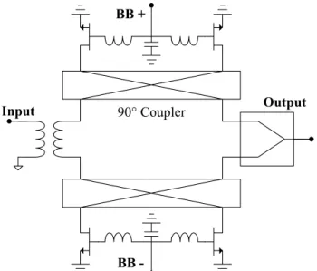
The schematic of the modified reflection-type BPSK modulator is shown in Fig. 1, which comprises a transformer, an in-phase combiner, and two bi-phase reflection modulators. BB+ and BB- are differential input ports for the baseband signal. The bi-phase reflection modulator consists of a 90° hybrid and two NMOS devices. By the imbalance analysis similar to the investigation in [11], the amplitude/phase imbalances of the transformer and in-phase combiner will be strongly relative to the amplitude/phase imbalances of the modulator, as well as the input reflection coefficient of the NMOS device. In general, the amplitude/phase imbalances of the in-phase combiner are very small due to its symmetric architecture. Therefore, the imbalances of the modulator will be dominated by the performance of the transformer. The insertion losses of the modulator are affected by the magnitude of the input reflection coefficient and the losses of the passive components.
BB +
BB -90° Coupler
Input Output
Fig. 1. Schematic of the modified reflection-type BPSK modulator.
For optimal design of the modulator, the device size of the NMOS was properly selected based on the on- and off-state reflection coefficients. In the design of the transformer in Fig. 1, we utilize a Marchand balun as 180° hybrid due to its excellent amplitude/phase match and broadband response. Two coupled lines in Marchand balun were constructed of broadside-coupled lines with the space and width of the striplines obtained from the required even- and odd-mode characteristic impedances. These two coupled lines were coiled up for a very compact area of 120
×
65 µm2. The 90° hybrid used for bi-phase reflection modulator was also implemented using broadside-coupled lines. The coupled lines of the broadside coupler were meandered to achieve a compact layout. The quarter-wave transmission lines in theWilkinson combiner were also meandered. In order to avoid the silicon substrate loss, the metal 1 (bottom layer) in the 1P8M CMOS process is used for ground plane, the metal 8 (top layer) is used for microstrip line, and the internal metal layers are used for broadside-coupled design and interconnection. All the passive components, including couplers, combiner and transmission line, are also simulated with a full-wave EM simulators [13]. The photograph of the modified reflection-type BPSK modulator is shown in Fig. 2 with a chip size of 0.5
×
0.35 mm2.Fig. 2. Photograph of the modified reflection-type BPSK modulator with a chip size of 0.5
×
0.35 mm2.III. MEASUREMENT RESULTS
The measurements of the modulator chips were performed via on-wafer probing. The S-parameters of the chips were measured by using an Agilent 8510C network analyzer, and the measured insertion losses of two states between 1 to 80 GHz for the modified reflection-type BPSK modulator are plotted in Fig. 3. The biases are 1 V at BB+ and 0 V at BB- for state 0; the biases are 0 V at BB+ and 1 V at BB- for state 1. For the turn-off state of the modulator, the biases at BB+ and BB- are both 0.5 V. The measured insertion losses are less than 13 dB and the isolation in turn-off state is better than 40 dB between 15 and 75 GHz. The amplitude and phase imbalances between state 0 and 1 is plotted in Fig. 4, which features an amplitude imbalance of within 0.5 dB and a phase imbalance of with 3° between 15 and 75 GHz. The worst-case input and output return losses are better than 8 dB.
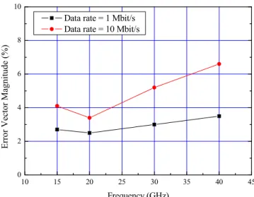
For the measurement of the modulation quality, an Agilent E8247C signal generator is used for local oscillator (LO) source. An Agilent E4448A spectrum analyzer and an Agilent vector signal analyzer are used as MMW down-converter and vector signal demodulator. The baseband signals are generated by using an Agilent E4438C vector signal generator, which is coded with a pseudorandom bit stream (PRBS). A root raised cosine (RRC) filter with a
0.5-α value is also applied to the baseband signals to minimize spectrum spread. The LO power is about 4 dBm and the baseband power is about -7 dBm. The measured EVM of BPSK modulation for the modified reflection-type BPSK modulator at 15, 20, 30 and 40 GHz is plotted in Fig. 5, which features an EVM of better than 3.5 and 7% for a data rate of 1 and 10 Mb/s, respectively. Assuming the channel bandwidth is 2 and 20 MHz for two data rates, the measured channel power is about -10 dBm for both two data rates. Due to the limitation of the baseband generator, the data rate can be only evaluated up to 50 Mb/s, and the measured output spectrum of the modified reflection-type BPSK modulator at 40 GHz is plotted in Fig. 6 with a channel power of -10 dBm within 100-MHz channel bandwidth. From the CW spectrum characterization, the modulation bandwidth of the modulator is wider than 1 GHz. Therefore, this modulator is suitable for broadband digital modulation applications.
0 10 20 30 40 50 60 70 80 -20 -18 -16 -14 -12 -10 -8 -6 -4 -2 0 Insertion Loss (dB) Frequency (GHz) State 0 State 1
Fig. 3. Measured insertion losses of two states between 1 to 80 GHz for the modified reflection-type BPSK modulator.
0 10 20 30 40 50 60 70 80 -3.0 -2.5 -2.0 -1.5 -1.0 -0.5 0.0 0.5 1.0 -5.0 -2.5 0.0 2.5 5.0 7.5 10.0 12.5 15.0 A m plitude Imba lnce (dB) Frequency (GHz) Ph as e Im ba la nce ( Deg re e)
Fig. 4. Amplitude and phase imbalances difference between state 0 and 1 for the modified reflection-type BPSK modulator.
10 15 20 25 30 35 40 45 0 2 4 6 8 10 Er ror V ec tor Ma gn itude (%) Frequency (GHz) Data rate = 1 Mbit/s Data rate = 10 Mbit/s
Fig. 5. Measured EVM of BPSK modulation for the modified reflection-type BPSK modulator at 15, 20, 30 and 40 GHz.
Fig. 6. Measured output spectrum of the modified reflection-type BPSK modulator at 40 GHz with a data rate of 50 Mb/s.
IV. CONCLUSION
An innovative topology for the reflection-type BPSK modulator was proposed and successfully implemented using standard bulk 0.13-µm CMOS process. This modulator achieves a RF frequency of 15-75 GHz, a modulation bandwidth of wider than 1 GHz with good amplitude/phase match, and an ultra compact chip size of 0.175 mm2. This bi-phase amplitude modulator can be further applied to an IQ modulator design for the high-level digital modulation applications. From this demonstration, it is observed that the CMOS technology has potential applications for low cost components in MMW regime.
ACKNOWLEDGEMENT
The work was supported in part by NTU-TSMC Joint-Development Project and the National Science Council of Taiwan, R.O.C. (NSC 2752-E-002-002-PAE, NSC 2219-E-002-016, NSC 2219-E-002-025 and NSC 93-2213-E-002-033). The chip was fabricated by TSMC, Hsinchu City, Taiwan, R.O.C.
REFERENCES
[1] Stephen A. Maas, The RF and Microwave Circuit Design
Cookbook, Artech House, Boston, 1998.
[2] Andrew Weetzei, “A stable 250 to 4000 MHz GaAs IQ modulator IC,” 1997 IEEE International Solid-State Circuits
Conference Digest, pp.364-365.
[3] Junji Itoh, Mitsuru Nishitsuji, Osamu Ishikaw and Daisuke Ueda, “2.1GHz direct-conversion GaAs quadrature modulator IC for W-CDMA base station,” 1999 IEEE International
Solid-State Circuits Conference Digest, pp.226-227.
[4] Esa Tiiliharju and Kari Halonen, “A 0.75-3.6 GHz SiGe direct-conversion quadrature-modulator,” 2003 European Solid-State
Circuits Conference, pp.565-568.
[5] Chung-Yu Wu and Hong-Sing Kao, “A 2-V low-power CMOS direct-conversion quadrature modulator with integrated quadrature voltage-controlled oscillator and RF amplifier for GHz RF transmitter applications,” IEEE Trans. on Circuit and
Systems, vol. 49, pp. 123-134, Feb. 2002.
[6] Tsunoo Tsukahara and Junzo Yamada, “3 to 5 GHz quadrature modulator and demodulator using a wideband
frequency-doubling phase shifter,” 2000 IEEE International Solid-State
Circuits Conference Digest, pp.384-385.
[7] Dennis C. W. Lo, Huei Wang, Barry R. Allen, G. S. Dow, Kwo Wei Chang, Michael Biedenbender, Richard Lai, Sian Chen and Daniel Yang, “Novel monolithic multifunctional balanced switching low-noise amplifiers,” IEEE Trans. on Microwave
Theory and Tech., vol. 42, pp.2629-2634, Dec. 1994.
[8] T. Lodhi, D.L. Edgar, H.McLelland, S.Ferguson, K.Elgaid, C.R. Stanley and I.G. Thayne, “A 77 GHz coplanar waveguide MMIC BPSK Vector Modulator realized using InP Technology,” 2000 IEEE Gallium Arsenide Integrated Circuit
Symposium Digest, pp.183-186.
[9] AliE. Ashtiani, Sueng-il Nam, Alex d’Espona, Stepan Lucyszyn and Ian D. Robertson, “Direct multilevel carrier modulation using millimeter-wave balanced vector modulators,” IEEE
Trans. on Microwave Theory and Tech., vol. 46, pp. 2611-2619,
Dec. 1998.
[10] S. Nam, N. Shala, K. S. Ang, A. E. Ashtiani, T. Gokdemir, I. D. Robertson and S. P. Marsh, “Monolithic millimeter-wave balanced bi-phase amplitude modulator in GaAs/InGaP HBT technology,” 1999 IEEE International Microwave Symposium
Digest, vol. 1, pp. 243-246.
[11] Hong-Yeh Chang, Tian-Wei Huang, Huei Wang, Yu-Chi Wang, Pane-Chane Chao, and Chung-Hsu Chen, “Broad-band BPSK and IQ modulator MMICs and millimeter-wave vector signal characterization,” IEEE Trans. on Microwave Theory and Tech., vol. 52, pp.908-919, Mar. 2004.
[12] Yi Sun, and Al P. Freundorfer, “A new overlay coupler for direct digital modulator in GaAs HBT,” IEEE Trans. on
Microwave Theory and Tech., vol. 52, pp.1830-1835, Aug. 2004.
[13] Sonnet User’s Manual, Release 9.0, Sonnet Software Inc., North Syracuse, NY, May 2003.
TABLE I
COMPARISON OF PREVIOULY REPORTED REFLECTYION-TYPE BPSK MODULATORS IN MMW AND THIS WORK
Author Device Approach Freq. Range
(GHz) Bandwidth (GHz) Chip Size (mm2) Imbalance Amp. (dB) Phase Imbalance (°) Mod. Bandwidth (MHz) D. C. W. Lo et al., [7] InP HEMT
Balanced reflection-type, Lange coupler 80-110 30 2.6
×
2.2 3 5 - D. C. W. Lo et al., [7] GaAs HEMTBalanced reflection-type, Lange coupler 25-44 19 3.5
×
2.4 3 5 - T. Lodhi et al., [8] InP HEMT Balanced reflection-type, CPW branch-line coupler 67-97 30 1.5×
2 - 7 - A. Ashtiani et al., [9] GaAs HEMTBalanced reflection-type, Lange coupler 30-40 10 1.1
×
1.5 - - 1 H. -Y. Chang et al., [11] GaAs HBTBalanced reflection-type, Lange coupler 45-90 45 1
×
1 2.5 4 >10 S. Sun et al., [12] GaAs HBT Balanced reflection-type, CPW overlay coupler 27-30 3 1.5×
0.8 0.5 3 1000This work CMOS Reflection-type, thin-film broadside 90° & 180° hybrids
15-75 60 0.5