A 24-GHz CMOS Current-Mode Power Amplifier
with High PAE and Output Power
Chung-Yu Wu, Shun-Wei Hsu, and Wen-Chieh Wang Nanoelectronics and Giga-scale Systems Laboratory, Institute of Electronics, National Chiao Tung University,
Room 307, Engineering Building 4th, 1001 Ta-Hsueh Road, Hsinchu City, Taiwan
Abstract—A new 24-GHz CMOS current-mode power
amplifier in 0.13-µm CMOS technology is proposed. By using the two-stage cascade current-mirror structure, the power amplifier has a maximum output power of 17.8 dBm, the OP1dB
of 13.8 dBm and the power gain of 23 dB under the supply voltage of 1.2V and the total power dissipation of 239 mW. As compared to other PAs at 17~24 GHz, the proposed current-mode PA has the highest power added efficiency (PAE) of 34.6% and the largest output power.
I. INTRODUCTION
Recently, the research on radio frequency (RF) ICs in 24-GHz-band has been accelerated because of the potential Industrial, Scientific, and Medical (ISM) band and the wireless vehicular radar applications [1]-[4]. It is known that CMOS technology is capable to implement RF transceivers at 24 GHz. The most critical key block in a CMOS 24-GHz RF transceiver is the power amplifier (PA). As compared with GaAs and pHEMT technologies, standard CMOS technology has the inherent characteristics of low unity-power-gain frequency and lossy on-chip passive elements. This makes the design of RF CMOS PAs with high output power and high power added efficiency (PAE) very challenging. Although the output power can be increased by utilizing multiple parallel transistors [5], the PAE cannot be increased in such a structure. To improve the PAE, several design techniques have been proposed. By using the special structure of transmission line and additional algorithms, the PAE of a RF CMOS PA can be improved to around 10% [6]-[7].
So far, all RF CMOS PAs have been designed in voltage-mode operation. However, current-voltage-mode design has the advantages of low-voltage operation and low power dissipation. Moreover, the overall amplifier gain comes from amplifying current instead of voltage. Thus the constraint on the upper limit of supply voltage can be avoided.
In this work, a new 24-GHz current-mode power amplifier is proposed and analyzed in 0.13-µm CMOS technology. From the simulation results, the proposed PA has 34.6% peak PAE at 17.8-dBm output power. As compared with other PAs at 17-24 GHz, the proposed
current-mode PA has the highest PAE and largest output power.
II. CIRCUIT DESIGN
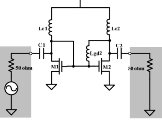
The proposed 24-GHz current-mode PA shown in Fig. 1 is designed in 0.13-µm CMOS technology. The MOS devices M1 and M2 form a driver-stage current mirror and M3 and M4 form an output-stage current mirror. The inductors Lc1, Lcb, and Lc4 are used to resonate with the gate capacitors of M1, M2/M3, and M4, respectively. The device capacitance between gate and drain of M2 (M4) is resonated by the inductor Lgd2 (Lgd4). Lgd2 and Lgd4 are used in both stages in order to obtain higher reverse isolation. The capacitor C1 and the inductor Lc1 serve as the input matching network. The capacitor C4 and the inductor L4 are the output impedance transfer network determined by load-pull simulation. Cp1 (Cp2) represents the capacitance of input (output) pad.
The MOS dimension of M4 in the output-stage current mirror shown in Fig. 2 is determined by the maximized power gain with the unity size of M3. To find the optimal size of M4, the width of MOS M4 is swept from 50µm to 400µm, with 50-µm steps. The 50-µm step is realized by multiplying 2.5-µm*20-fingers because 20-finger structure has the largest maximum available gain (MAG) at 24 GHz in 0.13-µm CMOS technology. Because the output stage is simulated without the driver stage, an additional input matching network L3 and C3 has been added in order to transfer the input impedance of the output stage to the 50-ohm input port. The ideal capacitor C4 is only used as a DC blocking. The optimized output impedance transfer network is determined by the load-pull simulation and not shown in Fig. 2. The values of C3, L3, Lc3, Lc4, and Lgd4 are re-determined for each sweeping step. Ideal inductors and capacitors are used in sweeping process for simplicity. The load-pull technique for output impedance transfer network is simulated after the dimensions of all components have been determined. In load-pull simulation, input power is manually changed to see the power gain, 1-dB compression point (P1dB), PAE at P1dB, peak PAE, input power corresponding to peak PAE, and maximum output power corresponding to that input power. The results are shown in Figs. 3 and 4.
2866 1-4244-0921-7/07 $25.00 © 2007 IEEE.
In Fig. 4, PAEP1dB means the PAE at P1dB and PeakPAE means maximum PAE, IPpeak means input power at peak PAE and OPmax means the maximum output power corresponding to IPpeak. As may be seen from Figs. 3 and 4, the OP1dB value is increased with the increasing width of M4. Further increasing the width, the power gain saturates. OPmax has the same trend as OP1dB.
Based on two reasons, the final choice of the width of M4 is 300 µm. The first reason is that OPmax should be kept not larger than 20 dBm [8]. The second one is to consider the current density of the inductor Lc4. After changing each ideal component to practical one, the performance parameters of the output stage can be obtained. The results are peak PAE of 53.9%, IPpeak of 11.9 dBm, and OPmax of 19.52 dBm.
Because the peak PAE operation is desired, a driver-stage shown in Fig. 5 is required to provide around 11.9-dBm input power to the output-stage current mirror. The sweeping process of the device size in the driver-stage current mirror is similar to that of device size in the output-stage current mirror. The sweeping range is from 10µm to 50µm, with 10-µm steps. Based on the required input power of the output-stage current mirror, the slave transistor width of 50µm in the driver-stage current mirror has been chosen. After using practical components, the driver-stage current mirror has peak PAE of 41.9 %, IPpeak of 5.8 dBm, and OPmax of 11.31 dBm.
According to the chosen device sizes in both stages, the impedance seen from the drain of MOS M3 is much smaller than the impedance seen from the drain of MOS M2 at 24 GHz. This property allows signal current going through without inter-stage matching network. Besides, two inductors Lc2 and Lc3 can be replaced by only one inductor Lcb to reduce physical area.
Figure 1. Two-stage current-mode power amplifier
Figure 3. Power gain and P1dB v.s. output-stage device size
Figure 4. PAE, IPpeak and OPmax v.s. output-stage device size
Figure 5. Driver-stage current mirror Figure 2. Output-stgae current mirror
III. SIMULATION RESULTS
The proposed CMOS current-mode PA of Fig. 1 is simulated by the Advanced Design System (ADS). All device models such as MOS, inductors, and capacitors are provided by 0.13-µm CMOS technology. The PA is operated at 1.2-V power supply with the total current of 199 mA.
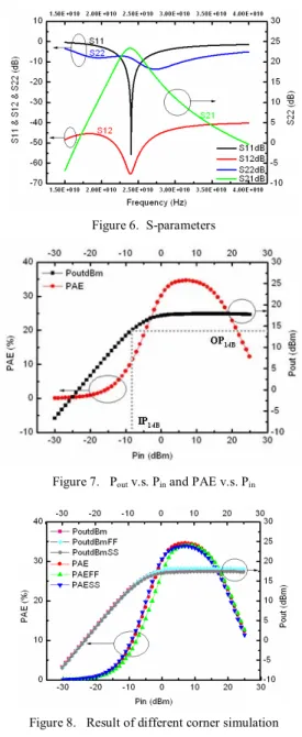
Fig. 6 shows S11, S12, S21 and S22 between 15 GHz to 40 GHz. S11 is -47 dB at 24 GHz and smaller than -15 dB between 23.4 GHz to 24.7 GHz. S12 is -65 dB at 24 GHz and lower than -40 dB between DC to 40 GHz. This is because inductors are used to resonate Cgd of both MOS M2 and M4 at 24 GHz. High reverse isolation keeps input-matching the same before and after the output impedance is loaded. S21 is 23.37 dB at 24 GHz and its 3-dB bandwidth is 3.3 GHz (23.3 GHz~25.6 GHz). S22, depending on output matching network, is around -8 dB. In the PA design, instead of conventional impedance conjugate matching, large signal output matching is considered. This leads to a low S22 value.
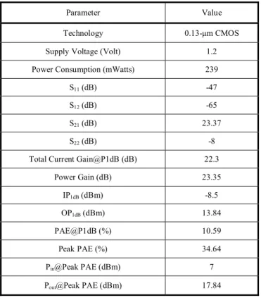
Output power and PAE versus input power is shown in Fig. 7 where the linear power gain (slope of Pout versus Pin) is 23.35 dB. Input- and output-refer 1-dB compression points are -8.5 dBm and 13.84 dBm, respectively. The PAE is 10.59 % at 1-dB compression point. The peak PAE is 34.64% with 7-dBm input power and 17.84-dBm output power. Slight difference between power gain and S21 comes from low S22 [9]. Because the optimized load impedances are different for both peak PAE and maximum output power as shown in Fig. 7, a trade-off between PAE and output power leads to the output power not as high as 19.52 dBm. Although the peak PAE occurs at the input power of 7 dBm, PAE can still be larger than 30 % when the input power is reduced to 0 dBm. The resultant decrease of output power is smaller than 0.5 dBm.
Different process corners and power supply variations have also been simulated. Corner simulations are performed by using FF, TT, and SS device parameters. Supply voltage variations are 1.4V, 1.2V, 1V and 0.8V. Figs. 8 and 9 are the simulation results. For the corner simulations of FF and SS, the simulated output power and PAE almost the same at FF and SS. For power supply variations, there is no change on power gain. The only change is the saturated output power and its corresponding PAE. From the above simulation results, it can be realized that the proposed CMOS current-mode PA is robust against both corner and power supply variations.
TABLE I is the performance summary of the proposed CMOS current-mode PA. TABLE II is the performance comparison to other silicon-based PAs. It can be seen that the proposed CMOS current-mode PA has the highest PAE and the largest output power among the RF PAs.
Figure 6. S-parameters
Figure 7. Pout v.s. Pin and PAE v.s. Pin
Figure 8. Result of different corner simulation
Figure 9. Result of power supply variation simulation
TABLE I. TWO-STAGE CURRENT-MODE PASUMMARY
Parameter Value
Technology 0.13-µm CMOS
Supply Voltage (Volt) 1.2 Power Consumption (mWatts) 239
S11 (dB) -47
S12 (dB) -65
S21 (dB) 23.37
S22 (dB) -8
Total Current Gain@P1dB (dB) 22.3 Power Gain (dB) 23.35 IP1dB (dBm) -8.5 OP1dB (dBm) 13.84 PAE@P1dB (%) 10.59 Peak PAE (%) 34.64 Pin@Peak PAE (dBm) 7
Pout@Peak PAE (dBm) 17.84
TABLE II. PERFORMANCE COMPARISONS OF SILICON-BASED POWER
AMPLIFIERS
Ref. [6] [10] [11] [12] Work This Technology 0.18-µm CMOS 0.18-µm CMOS SiGe HBT 0.13-µm CMOS 0.13-µm CMOS
Frequency (GHz) 24 24 24 17 24 Supply Voltage (Volt) 2.8 2.5 5V 1.5 1.2 S11/S12 (dB) -6.9/-40 -/- -/- -/- -47/-65 Power Gain (dB) 7 - 18 4 23.35 DC Power (mWatts) 280 170 550 75 239 OP1dB (dBm) 11 11 - 4.2 13.84 PAE@P1dB (%) 4.45 - - 3.45 10.59 Peak PAE (%) 6.5 6.5 3 - 34.64 Sat. Pout (dBm) 14.5 14 12 - 17.84
Topology 2-Stage CSCG 2-Stage CSCG CS differential 3-Stage CS differential 2-Stage N-type Current Mirror 2-Stage Note Operation P1dB Operation P1dB Peak PAE Operation Operation P1dB
Peak PAE Operation
IV. CONCLUSION
This paper presents a 24-GHz CMOS current-mode power amplifier in 0.13-µm technology. The PA uses 1.2-V supply voltage and the total power consumption is 239 mW. Its linear power gain is 23.35 dB, output power is 17.84 dBm, and PAE can be achieved as high as 34.64 % at the same time. Corner and supply voltage variations have also been considered. The simulation results have shown that the proposed current-mode PA is robust under these variations. The proposed CMOS current-mode PA is now under fabrication.
ACKNOWLEDGMENT
This work was supported by the National Science Council (NSC), Taiwan, under the Grant NSC-95-2221-E-009-292. The authors would like to thank the Chip Implementation Center (CIC), National Applied Research Laboratory, for the fabrication of testing chip. The authors would also like to thank the support of HFSS from Ansoft Taiwan.
REFERENCES
[1] Federal Communications Commission FCC 02-04, Section 15.249 [2] Federal Communications Commission FCC 02-04, Section 15.515 [3] Ian Gresham, Alan Jenkins, Robert Egri, Channabasappa
Eswarappa, Frank Kolak, Ratana Wohlert, Jacqueline Bennett. J-P Lanteri, “Ultra Wide Band 24GHz Automotive Radar Front-End,” in IEEE MTT-S Int. Microwave Symp. Dig., 2003, pp. 369-372 [4] Hiroyo Ogawa, “24-GHz Ultra-Wideband Short-Range Impulse
Radar for Vehicular Applications”, in IEEE CCNC, 2006, pp. 696-700
[5] E. Afshari, H. Bhat, X. Li, and A. Hajimiri, “Electrical funnel: a broadband signal combining method,” in IEEE Int. Solid-State Circuits Conf. (ISSCC) Dig. Tech. Papers, Feb. 2006, pp. 206–207. [6] A. Komijani and A. Hajimiri, “A 24 GHz, +14.5 dBm fully-integrated power amplifier in 0.18 _m CMOS,” in Proc. IEEE Custom Integrated Circuits Conf., Oct. 2004, pp. 561–564
[7] Abbas Komijani, and Ali Hajimiri, “A Wideband 77-GHz, 17.5-dBm Fully Integrated Power Amplifier in Silicon,” in IEEE Journal of Solid-State Circuits (JSSC), VOL. 41, NO. 8, AUGUST 2006, pp. 1749-1756
[8] ETSI EN 302 288-1 V1.1.1
[9] Guillermo Gonzalez, Microwave Transistor Amplifiers Analysis and Design, 2nd ed. Prentice Hall
[10] A. Natarajan, and A. Hajimiri, “A fully Integrated 24-GHz Phased-Array Transmitter in CMOS,” in IEEE Journal of Solid-State Circuits (JSSC), VOL. 40, NO. 12, DECEMBER 2005, pp. 2502-2514
[11] Noyan Kinayman, “Design of 24 GHz SiGe HBT Balanced Power Amplifier for System-on-a-Chip Ultra-Wideband Applications,” Radio Frequency Integrated Circuits Symposium, 2005
[12] M. Tiebout, “17 GHz Transceiver Design in 0.13 um CMOS,” Radio Frequency Integrated Circuits Symposium, 2005