630 IEEE ELECTRON DEVICE LETTERS, VOL. 35, NO. 6, JUNE 2014
Characterization of Oxygen Accumulation
in Indium-Tin-Oxide for Resistance
Random Access Memory
Rui Zhang, Kuan-Chang Chang, Ting-Chang Chang, Tsung-Ming Tsai, Syuan-Yong Huang, Wen-Jen Chen,
Kai-Huang Chen, Jen-Chung Lou, Jung-Hui Chen, Tai-Fa Young, Min-Chen Chen, Hsin-Lu Chen,
Shu-Ping Liang, Yong-En Syu, and Simon M. Sze
Abstract— In this letter, we report the oxygen accumulation
effect and its influence on resistive switching for gadolinium-doped silicon dioxide (Gd:SiO2) resistance random access
memory (RRAM). We find that oxygen absorbance by indium-tin-oxide electrode affects the conduction current mecha-nism, and remarkably modifies the device performance of RRAM devices. By current fitting, Schottky emission can be observed in both low and high resistance states, from which conduction model is proposed to clarify the oxygen accumulation phenomenon. Reliability tests, including endurance and high temperature retention are further carried out, evaluating the significance of oxygen accumulation effect in redox reaction for RRAM devices.
Index Terms— Oxygen accumulation, indium tin oxide, Schottky emission, RRAM.
I. INTRODUCTION
R
ECENTLY, various electronic devices and systems on panel (SOP) technology were widely developed and investigated. For the concept of SOP, amorphous silicon (α-Si) and poly-crystal silicon (poly-Si) thin-film transistors (TFT) [1], [2] for transparent active matrix LCD display and storageManuscript received March 8, 2014; revised March 25, 2014; accepted April 8, 2014. Date of publication April 24, 2014; date of current version May 20, 2014. This work was supported by the National Science Council of Taiwan under Contract NSC-102-2120-M-110-001. The review of this letter was arranged by Editor T. San. (Corresponding authors: T. C. Chang and
K. H. Chen.)
R. Zhang and J.-C. Lou are with the School of Software and Microelec-tronics, Peking University, Beijing 100871, China.
K.-C. Chang, T.-M. Tsai, and S.-Y. Huang are with the Department of Materials and Optoelectronic Science, National Sun Yat-Sen University, Kaohsiung 80424, Taiwan.
T.-C. Chang is with the Department of Physics, National Sun Yat-Sen University, Kaohsiung 80424, Taiwan, and also with the Advanced Opto-electronics Technology Center, National Cheng Kung University, Tainan 701, Taiwan (e-mail: [email protected]).
W.-J. Chen is with the Department of Electrical and Computer Engineering, University of Texas at Austin, Austin, TX 78712 USA.
K.-H. Chen is with the Department of Electronics, Tung Fang Design University, Kaohsiung 829, Taiwan (e-mail: [email protected]).
J.-H. Chen is with the Department of Chemistry, National Kaohsiung Normal University, Kaohsiung 824, Taiwan.
T.-F. Young, H.-L. Chen, and S.-P. Liang are with the Department of Mechanical and Electro-Mechanical Engineering, National Sun Yat-Sen Uni-versity, Kaohsiung 80424, Taiwan.
M.-C. Chen and Y.-E. Syu are with the Department of Physics, National Sun Yat-Sen University, Kaohsiung 80424, Taiwan.
S. M. Sze is with the Department of Electronics Engineering, National Chiao Tung University, Hsinchu 300, Taiwan.
Color versions of one or more of the figures in this letter are available online at http://ieeexplore.ieee.org.
Digital Object Identifier 10.1109/LED.2014.2316806
devices were widely discussed for the wider application and future development of consumer electronic products [3], [4].
Numerous nonvolatile memories devices such as the ferroelectric random access memory (FeRAM) [5], magnetic random access memory (MRAM) [6], phrase change memory (PCM) [7] and RRAM [8], [9] have been widely investigated for the future applications in portable electrical products. Worldwide researchers have spent great efforts on the investi-gation of RRAM. Here in this research, we mainly focus on the silicon oxide based system for the advantage of compat-ibility of low-cost silicon oxide to IC process and its natural stable electrical property. Especially, multiple RRAM working parameters like programming voltage, power consumption and endurance can be effectively improved by combining the metal doping in silicon oxide and the oxygen deficient electrode, which cannot be obtained in the pure silicon oxide RRAM [10], [11].
We applied indium-tin-oxide (ITO), the vastly investi-gated transparent material, into RRAM and characterized its influence on the redox reaction of resistive switching devices. Specially, we pay attention to the role of indium tin oxide working as the electrode rather than the switching layer, from which we find oxygen accumulation behavior. The accumu-lated oxygen will affect the conduction mechanism and espe-cially the performance of RRAM device. From our research, we find the electrode influences the device working character-istics and the chemical element composition of the electrode actively affects the RRAM resistive switching behavior.
II. EXPERIMENTALSETUP
In this letter, the Gd:SiO2 RRAM device was fabricated to
investigate the effect of ITO on filament-type RRAM device using metal doped silicon oxide as resistive switching layer. The role of Gd doping is to induce the conductive filament formation in the SiO2 according to our previous study. The
Gd co-sputtering with SiO2 was deposited on the patterned
TiN/Ti/SiO2/Si substrate with pure SiO2 and gadolinium
tar-gets. The switching layer was 20-nm-thick and the sputtering power was fixed with RF power 200W and DC power 10W for silicon dioxide and gadolinium targets, respectively. In addition, the ITO top electrode with a thickness of 200 nm was deposited on Gd:SiO2 film to form ITO/Gd:SiO2/TiN
sandwich structure by DC magnetron sputtering. The via
0741-3106 © 2014 IEEE. Personal use is permitted, but republication/redistribution requires IEEE permission. See http://www.ieee.org/publications_standards/publications/rights/index.html for more information.
ZHANG et al.: CHARACTERIZATION OF OXYGEN ACCUMULATION IN INDIUM-TIN-OXIDE 631
Fig. 1. The typical bipolar switching behavior of the Gd:SiO2RRAM devices
with ITO electrode. The bottom left and right insets show the schematic measurement method and forming I-V curve, respectively.
Fig. 2. FTIR spectrum of the Gd:SiO2 film measured in middle-infrared
region. The inset shows the via structure of ITO/Gd:SiO2/TiN RRAM device. structure (shown in Fig. 2) is for the strict control of device size and the uniformity of electrical properties. All the elec-trical measurements were conducted by an Agilent B1500A semiconductor analyzer.
III. RESULTS ANDDISCUSSION
Before standard electrical measurements, the RRAM devices should be operated with a forming process [8], [9] and the devices were switched from high resistance state (HRS) to low resistance state (LRS) at a voltage of −5.4V with 1μA compliance current (right inset of Fig. 1). The voltage sweep bias was applied on the TiN electrode with the ITO electrode grounded. After that, DC sweeping test was conducted to investigate the influence of ITO top electrode on Gd:SiO2
RRAM devices, from which bipolar resistance switching char-acteristics were obtained, as shown in Fig. 1. From the current-voltage curve, a special advantage for the ITO/Gd:SiO2/TiN
RRAM device can be observed, which is the low power consumption. The device can be operated within the small voltage range from−0.7V to 0.7V and Set at merely −0.2V. In order to confirm the material properties of Gd:SiO2 thin
film, Fourier transform infrared (FTIR) spectroscopy was used to investigate the chemical bonding of the Gd:SiO2film in this
Fig. 3. Conduction current fitting results and the corresponding fitting goodness.
letter. Figure 2 shows that Gd–O stretch bonding was found in the Gd:SiO2 film at 559cm−1 and 461cm−1 from FTIR
spectrum [12], [13]. These two picks ascribe to the stretching vibrations of Gd-O, this mainly owes to the amorphous film structure fabricated by sputter As the film is not perfect single crystalline structure, the Gd-O chemical bonding is not stress-free type bonding. In addition, the antisymmetric stretch mode of Si–O–Si bonds can be observed at 1041cm−1. According to these absorption peaks expressed in FTIR spectra, we can confirm that the Gd element was bonded with the oxygen element in the SiO2 film.
To further understand the conduction mechanism, current fittings of LRS and HRS were conducted, as shown in Fig. 3. We can obtain Schottky emission [14] conduction in both HRS and LRS, and the figures in the right side of Fig. 3 are their corresponding fitting goodness. The fitting results imply that the major leakage current originates from the electrons surpassing the potential energy barrier between the interface of the switching layer and the electrode by thermionic effect. Owing to the unequal barrier heights, I-V curve will demonstrate asymmetric property, which can be distinguished from Poole-Frenkel. The device conduction mechanism can be predominantly influenced by the switching layer thickness and the introduction of metal dopants in the switching layer, for this will particularly influence the defects distribution and thus affects the formation of conduction path. Unlike the thick undoped silicon oxide RRAM [15], which needs high operation voltage (-10V–10V) to realize bipolar switch, the Gd doped silicon oxide RRAM can be switched within
−0.7V−0.7V for the help of metal ions in the formation
process of conduction path.
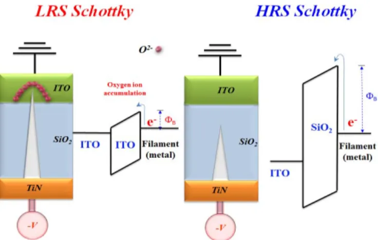
According to the above-mentioned electrical and material analyses, we propose a model to explain the influence of ITO for the special asymmetric set and reset process in the ITO/Gd:SiO2/TiN RRAM devices, as shown in Fig. 4.
During the set process, the conductive filament grew towards to the ITO electrode by driving oxygen ions to ITO electrode. As lots of oxygen vacancies exist in the ITO thin film, oxygen ions driving force orients to the ITO side. Enhanced by the concentration gradient, together with electrical driving force,
632 IEEE ELECTRON DEVICE LETTERS, VOL. 35, NO. 6, JUNE 2014
Fig. 4. Conduction model and relative energy band diagrams for LRS and HRS in the ITO/Gd:SiO2/TiN structure RRAM.
Fig. 5. (a) Retention performance at 85 °C and (b) Endurance properties of Gd:SiO2RRAM device. The reading voltage was set as 0.1V.
oxygen ions can be more easily propelled into the ITO elec-trode, thus we can obtain smaller set voltage compared with traditional single voltage driven force device. The current con-duction mechanism in LRS dominated by Schottky emission conduction is due to electron carrier surmounting the barrier height between filament and ITO semiconductor layer. The semiconductor ITO around the filament tip originates from the high oxygen accumulation effect, in which original conductive ITO will be locally oxidized by oxygen ions propelled by the double driving force, which is shown schematically in Fig. 4. This process will results in the ITO energy band-gap widen effect, for the formation of semiconductor-like ITO [16]. As for the reset process, the conductive filament will be oxidized and ruptured, making the current conduction path blocked by silicon oxide. Due to the high energy barrier height of silicon oxide, less carriers can surpass the barrier and thus LRS is switched to HRS. Therefore, the carrier conduction mechanism of HRS in the Gd:SiO2RRAM also complies with
Schottky emission, originating from carrier overcoming the barrier height between filament and Gd:SiO2 film, shown in
the right diagram of Fig. 4.
To further verify the influence of oxygen accumulation effect on ITO/Gd:SiO2/TiN RRAM devices, retention and
endurance properties were measured. As shown in Fig. 5(a), no significant changes in the resistance values of LRS and HRS were observed even after 104 second retention test at 85 °C. The reading voltage was set at 0.1V. Furthermore, the endurance properties were measured by continuous switch-ing cyclswitch-ing as shown in Fig. 5(b). We find the resistance ratio between HRS and LRS remain stable during 109 pulse
cycling operations. This is the first time for single switching layer silicon oxide based RRAM reaching 109 endurance performance, and this also gives us guidance for RRAM performance improvement. By applying ITO, we can utilize the oxygen accumulation effect to better control the reduction and oxidation process.
IV. CONCLUSION
In conclusion, the influence of oxygen accumulation effect in ITO electrode for bipolar resistance switching properties of the Gd:SiO2 RRAM devices were investigated and discussed
in this letter. Schottky emission conduction in both LRS and HRS are depicted, from which we find the Schottky conduction mechanism originates different barrier height between the filament and electrode. Outstanding performance including stable high temperature retention and 109 endurance further unveils the importance for the selection of electrode material, and this also enlightens us one simple way to manipulate oxygen ions in resistive devices.
ACKNOWLEDGMENT
This work was performed at National Science Council Core Facilities Laboratory for Nano-Science and Nano-Technology in Kaohsiung-Pingtung area, NSYSU Center for Nano-Science and Nano-Technology.
REFERENCES
[1] R. A. Street, “Thin-film transistors,” Adv. Mater., vol. 21, no. 20, pp. 2007–2022, 2009.
[2] M. C. Chen et al., “A low-temperature method for improving the perfor-mance of sputter-deposited ZnO thin-film transistors with supercritical fluid,” Appl. Phys. Lett., vol. 94, no. 16, p. 162111, 2009.
[3] T. C. Chang et al., “Developments in nanocrystal memory,” Mater.
Today, vol. 14, no. 12, pp. 608–615, Dec. 2011.
[4] T. C. Chen et al., “Light-induced instability of an InGaZnO thin film transistor with and without SiOx passivation layer formed by plasma
enhanced chemical vapor deposition,” Appl. Phys. Lett., vol. 97, no. 19, pp. 192103-1–192103-3, 2010.
[5] T. P. Ma and J. P. Han, “Why is nonvolatile ferroelectric memory field-effect transistor still elusive?” IEEE Electron Device Lett., vol. 23, no. 7, pp. 386–388, Jul. 2002.
[6] S. Tehrani et al., “Magnetoresistive random access memory using magnetic tunnel junctions,” Proc. IEEE, vol. 91, no. 5, pp. 703–714, May 2003.
[7] M. Wuttig and N. Yamada, “Phase-change materials for rewriteable data storage,” Nature Mater., vol. 6, no. 11, pp. 824–832, 2007.
[8] R. Waser and M. Aono, “Nanoionics-based resistive switching memo-ries,” Nature Mater., vol. 6, no. 11, pp. 833–840, 2007.
[9] R. Waser et al., “Redox-based resistive switching memories-nanoionic mechanisms, prospects, and challenges,” Adv. Mater., vol. 21, nos. 25–26, pp. 2632–2663, 2009.
[10] A. Mehonic et al., “Resistive switching in silicon suboxide films,”
J. Appl. Phys., vol. 111, no. 7, pp. 074507-1–074507-9, 2012.
[11] J. Yao et al., “Resistive switches and memories from silicon oxide,”
Nano Lett., vol. 10, no. 10, pp. 4105–4110, 2010.
[12] R. Thangappana et al., “Fabrication of Gd2O3 nanofibers by
electro-spinning technique using PVA as a structure directing template,” Appl.
Surf. Sci., vol. 261, pp. 770–773, Nov. 2012.
[13] A. Garbout et al., “Structural, FT-IR, XRD and Raman scattering of new rare-earth-titanate pyrochlore-type oxides LnEuTi2O7(Ln = Gd, Dy),” J. Alloys Compounds, vol. 573, pp. 43–52, Oct. 2013.
[14] S. M. Sze and K. K. Ng, Physics of Semiconductor Devices. New York, NY, USA: Wiley, 2006.
[15] A. Mehonic et al., “Electrically tailored resistance switching in silicon oxide,” Nanotechnology, vol. 23, no. 45, p. 455201, 2012.
[16] C. Guillén and J. Herrero, “Influence of oxygen in the deposition and annealing atmosphere on the characteristics of ITO thin films prepared by sputtering at room temperature,” Vacuum, vol. 80, no. 6, pp. 615–620, 2006.