室溫紅外線偵檢器與圓形極化天線在無線微感測器應用上的設計,製作與模擬分析
219
0
0
全文
(2) 室溫紅外線偵檢器與圓形極化天線在無線微感測器應用上的設計,製 作與模擬分析 Design, Fabrication and Simulation of Uncooled Infrared Detectors and Circularly Polarized Antennas for Wireless Micro-Sensor Applications 研 究 生:林稔杰. Student:Da-Ming Fan. 指導教授:張國明 博士. Advisor:Dr. Kow-Ming Chang. 鄧一中 博士. Dr. I-Chung Deng. 國 立 交 通 大 學 電 子 工 程 學 系 電 子 研 究 所 博 士 論 文. A Dissertation Submitted to Department of Electronics Engineering & Institute of Electronics College of Electrical Engineering and Computer Science National Chiao Tung University In Partial Fulfillment of the Requirements For the Degree of Doctor of Philosophy In Electronics Engineering July 2007 Hsinchu, Taiwan, Republic of China. 中華民國九十六年七月.
(3) 室溫紅外線偵檢器與圓形極化天線在無線微感測器上的 設計,製作與模擬分析. 研究生 : 林稔杰. 指導教授 : 張國明 博士 鄧一中 博士 國立交通大學 電子工程學系電子研究所. 摘要. 一個無線微感測器主要可以分為三個部分:天線、積體電路以及感測器。一般 而言,由於積體電路以及感測器所占面積相對於天線尺寸顯得相當的微小,因此,一 個無線微感測器所佔有的面積主要由天線的大小來做決定。此外,對於一個無線微 感測系統而言,系統的功率損耗以及系統的傳輸距離在設計時都必須加以考慮進 去。本論文主要針對如何製作用來感測物體溫度的室溫紅外線偵檢器以及如何製作 一個可與積體電路與感測器整合的圓形極化天線,此外對於無線微感測器的傳輸距 離以及射頻訊號的轉換特性都做了一些評估。因此本論文主要分成三個部分:第一部 分為"無線微感測系統的效能評估";第二部分為"低溫 CMOS 製程相容之室溫紅線 感測器的設計與模擬分析";第三部分為"適用於無線微感測器之圓形極化槽孔天 線設計與模擬分析"。 在第一部分中,為了降低系統的功率損耗以及有效利用接收到的電磁波能量, 我們利用無線射頻辨識技術(RFID)來製作一個零偏壓的天線整流器(rectenna),此 天線整流器的輸出受到訊號傳輸距離的影響,為了精確評估電磁波能量的接收以及 高頻訊號的轉換,因此我們利用高頻 3D 電磁場軟體以及高頻電路軟體來模擬收發系 統間的訊號傳輸特性。 1.
(4) 在第二部分中,我們為了使積體電路與微感測器之間的訊號損耗降低以及增加 感測訊號的靈敏度,我們採用在積體電路製作完成後於其上實現我們的紅外線微感 測器。爲了達到此一目標,我們必須將整個元件陣列的製程溫度限制在低於 400 oC, 同時配合面型微細加工技術以及 CMOS 製程相容的方法來縮小每個紅外線感測陣 列的像素面積以及降低元件的製作成本,進而提高系統的解析度以及增加陣列元件 的積集度。在元件材料選擇上,我們採用二氧化矽當作元件的結構層、鋁當犧牲層、 摻雜的非晶矽當作感測材料層、鉭用來當做金屬訊號傳導層,同時利用另一薄鋁層 當作反射層來製作四分之一波長共振腔增加紅外線的吸收率,此元件的材料選擇可 以達到幾乎百分之百的蝕刻選擇比,對於元件的製程上是相當穩定。此外,在元件 最後乾燥過程中,我們也探討如何利用現有簡單的熱板設備取代目前常用的昂貴二 氧化碳超臨界點來達到元件的高良率以及高可靠度,以利元件的進一步大量製造。 對於元件的結構分析,我們使用 CoventorWare 軟體,在元件犧牲層釋放過程中,用 來預測整個元件的浮板結構變形狀況,進一步用來判斷浮板懸浮與否。對於元件的 熱分析,我們使用 Ansys 有限元素分析軟體來計算元件的溫度分布、熱時間常數以 及熱流通量。 就天線而言,目前大部分的無線微感測器大都利用線性極化天線來傳輸感測訊 號,線性極化天線往往因為傳輸端與接受端的天線角度誤差,而造成傳輸系統的極 化損耗,最大損耗可達 30dB,然而對於圓形極化系統而言則可以避免此一損耗產 生。圓形極化天線在設計上比線性極化天線困難很多,加上目前尚未有縮小化圓形 極化天線出現過,因此對於圓形極化天線研究的人更少。目前大部分圓形極化天線 主要以微帶天線居多,主要是因為微帶天線在設計上槽孔天線容易,然而槽孔天線 卻有比微帶天線更寬的阻抗頻寬、圓形極化頻寬。在第三部分中,我們在目前常用 的商業基板 FR4(介電常數 4.4,厚度 1.6 mm,基板損耗正切 0.0245)上創新設計出許 多不同類型的圓形極化行波槽孔天線,有別於傳統的圓形極化共振型槽孔天線。這 些圓形極化行波槽孔天線操作於 2.4 GHz ~2.5 GHz 頻段範圍,S 參數都低於 -30 dB,天線輻射增益都在 3 dBi 以上,天線輻射效率大於 85%,以及 3 dB 圓形極化軸 2.
(5) 比在空間分部至少涵蓋正負 30 度以上的俯角,而饋入的方式有微帶線訊號饋入以及 共平面波導訊號饋入兩種,天線輸入阻抗匹配到射頻系統的 50 歐姆。我們藉由電磁 模擬軟體 Zeland IE3D 來進行 2.5D 的天線設計與模擬分析,接著利用 Ansoft HFSS 來觀察天線 3D 結構的電磁分佈,這是因為 IE3D 對於開發平板天線的時效上有其優 勢,而 HFSS 對於空間中的電磁分佈有其獨到之處。天線阻抗量測部分使用網路分 析儀,而輻射場形部分使用 HP85301C 於無反射波量測實驗室進行。. 關鍵字 : 無線微感測器、紅外線感測器、CMOS 製程相容、圓形極化天線、行波天 線、槽孔天線. 3.
(6) Design, Fabrication and Simulation of Uncooled Infrared Detectors and Circularly Polarized Antennas for Wireless Microsensor Applications. Student: Ren-Jie Lin. Advisor: Dr. Kow-Ming Chang Dr. I-Chung Deng. Department of Electronics Engineering & Institute of Electronics National Chiao-Tung University HsinChu, Taiwan R.O.C.. Abstract. A wireless microsensor can be divided into three main parts: Antenna, integrated circuit (IC), and micro-sensor. Generally, the total area of IC and micro-sensor is very little as compared with the antenna area, and therefore the area of a wireless microsensor is dependent on the antenna area. Besides, for a wireless microsensing system, the power loss of a system and the transmission distance must be taken into account during the system design. The purpose of this dissertation focus on how to fabricate the uncooled infrared detector array using to sense the infrared from objects and how to develop the circularly polarized slot antenna using to integrate with IC and micro-sensor. Besides, we also evaluate the transmission distance and the RF signal conversion characteristics of the wireless microsensing system. Consequently, this dissertation includes three parts: Part I “Performance evaluation of wireless microsensing system”; Part II “Design and simulation of an uncooled microbolometer with low temperature CMOS-process compatibility”, Part III “Design and simulation of circularly polarized slot antennas for wireless micro-sensor applications”. 4.
(7) In Part I, in order to decrease the system power loss and increase efficiently the use of the received electromagnetic power, we use the radio frequency identification technology (RFID) to design a zero-bias rectenna (antenna and rectifier). The output of the rectenna is affected by the signal transmission distance. In order to exactly estimate the received EM power and RF signal conversion, we use a 3-D high frequency EM software and a high frequency circuit software to simulate the signal transmission characteristics between the transmitter and the receiver. In Part II, in order to reduce the signal loss and increase the sensing signal sensitivity between IC and micro-sensor, we implement our infrared micro-sensor directly fabricated on the top of IC. Achieving the preceding purpose, the whole processing temperature must be limited to below 400 degrees. At the same time, the surface micromachining technology and CMOS-process compatible method used to reduce the pixel size of infrared sensor array and lower the device-processing cost can further improve the system resolution and increase the device fill factor. With respect to material selection, we use silicon dioxide as the structural layer, Al as sacrificial layer, doped amorphous silicon as the sensitive layer, and Ta as the signal conducting line. Besides, we also use aluminum as a mirror layer to develop a quarter-wavelength resonator to increase infrared absorption. These materials providing nearly 100% etching selectivity is very stable during device fabrication. In addition, we also discuss how to use simple and cheap hot plate instead of expensive apparatus of CO2 supercritical to achieve high yield and high reliability during device drying step. This is a great benefit to mass production. Considering device structural analysis, we use CoventorWare simulator to predict the status of the device structure deformation to further determine whether the membrane is suspend or collapsed during device releasing step. With respect to thermal simulation, Ansys which is a FEM simulator is used to estimate the temperature distribution, thermal time constant, and heat flux distribution of the device. 5.
(8) In terms of antenna, nowadays the most use of antenna communicating signal for wireless micro-sensor is the linearly polarized antenna. However, the polarization misalignment between the antennas of the transmitter and receiver always results in polarization loss, the maximum loss being 30dB possible. But with respect to circularly polarized (CP) system, the polarization loss can be alleviated. Only a few of the studies related to circularly polarized antenna are done due to the difficulty of the CP antenna. In addition, the compact size of CP antenna is never presented. Because the CP microstrip antennas are easier design than the CP slot antennas, the most of CP antennas are microstrip antenna. However, the slot antenna has wider impedance bandwidth, axial-ratio bandwidth over the microstrip antenna. In Part III, we develop several novel design CP traveling wave slot antennas on the common use substrate of FR4 (dielectric constant of 4.4, height of 1.6 mm, and loss tangent of 0.0245), and these proposed slot antennas are different from other traditional CP resonator slot antenna. These proposed slot antennas have several characteristics such as the operating frequency of 2.4 ~2.5 GHz, the S parameter of lower than -30 dB, the antenna gain above 3 dBi, the antenna radiation efficiency of above 85 %, and the 3 dB Axial-ratio at least cover the 30 degrees at the elevation direction. The feed types of the proposed antennas include microstrip feed and coplanar waveguide (CPW) feed. The Antenna input impedance also matches to 50 Ohm of the general RF system. We use electromagnetic simulator of Zeland IE3D to design and simulate the 2.5D antenna structure followed by using Ansoft HFSS to observe the 3D electromagnetic distribution. This is because the IE3D is superior to HFSS in analyzing time. However, the HFSS can exactly display the 3D electromagnetic distribution in the free space. The antenna impedance is measured by network analyzer, and the radiation pattern is measured by HP 85301C in the non-reflection chamber. Keyword: Wireless micro-sensor, Infrared detector, CMOS process compatible, circularly polarized antenna, traveling wave antenna, slot antenna 6.
(9) 致謝 ( Acknowledgements). 首先誠摯的感謝指導教授張國明博士多年來的悉心指導與照顧,使我得以相繼 完成碩士與博士學位,在這段攻讀博士學位的過程中,深刻的體會到老師的淵博學 識、廣闊的學術視野、嚴謹認真的致學態度,這些不僅令我在學術上有所精進,在 待人處事上更是受益良多。在這求學七年期間,老師能夠讓我盡情發揮自己的研究 理念與擴展多方位的研究領域,讓我得以沉醉在研究的喜悅之中,讓我了解到自由 發揮創意所帶來的無限空間,同時也很感激老師在學生低潮時期的拉拔與提攜,讓 學生重獲研究的動力。此外,也誠摯的感謝共同指導教授鄧一中博士在研究資源上 與研究方法建言上提供莫大的幫助與方便。 修業期間,特別感謝實驗室一同打拼的學長、學弟,尤其是已畢業學長羅俊傑 在紅外線感測器上對我的協助與解惑,也感謝學弟黃士軒、林建宏與陳博寧在這段 時間一起努力於學術研究與空閒時間的團隊激戰。另外,對於國家奈米元件實驗室、 交大奈米中心的技術員徐秀鑾、范秀蘭、陳悅婷與黃月美小姐以及葉雙得先生多年 來在半導體製程設備上的幫助與方便,讓我可以順利的將論文完成。 最後,必須感謝我的家人,感激你們這麼多年來的支持與幫忙,讓我無後顧之 憂的在學術研究上努力,在我失意的時候也給我適時的鼓勵,真的感激你們。. 7.
(10) Contents Part I .............................................................................................................. 10 Part II ............................................................................................................ 10 Part III........................................................................................................... 13 Introduction.................................................................................................. 17 Part I .............................................................................................................. 21 Chapter 1 Electromagnetic power transmission ..................................................................... 22 Chapter 2 Rectifier of a wireless microsensor ......................................................................... 28. Part II ............................................................................................................ 40 Chapter 1 Introduction.............................................................................................................. 41 1.1 Characteristics of infrared ........................................................................ 41 1.2 Infrared (IR) detector................................................................................ 42 1.3 Micromachining technology with integrated circuits for micro-sensor applications…………………………………………………………………...43 1.4 Surface micromachining on top of IC for bolometer detector applications …………………………………………………………………..46 1.5 In our research …………………………………………………………..48 Chapter 2 Bolometer Operation and Theory .......................................................................... 49 2.1 Bolometer operation .................................................................................. 49 2.2 General performance concepts [23] ......................................................... 51 2.3 Analysis of heat transfer mechanisms for bolometer structures ........... 55 2.4 Material property control ......................................................................... 58 Chapter 3 Structure design and related considerations ......................................................... 59 3.1 General considerations .............................................................................. 59 3.2 Consideration about material of sensing layer ....................................... 61 3.3 Consideration about micromachining technology .................................. 66 3.4 Consideration about material of sacrificial layer ................................... 67 Chapter 4 Device thermal simulation ...................................................................................... 70 Chapter 5 Device fabrication .................................................................................................... 93 5.1 Processes of bolometer array .................................................................... 93 8.
(11) 5.2 Detailed processing list .............................................................................. 97 5.3 Some important considerations about drying process ........................... 98 Chapter 6 Results and Discussion .......................................................................................... 106 Chapter 7 Summary ................................................................................................................ 121. Part III......................................................................................................... 128 Chapter1 Introduction............................................................................................................ 129 1.1 Antenna polarization review for signal communication ...................... 129 1.2 Microstrip antenna for circular polarization (CP) ............................... 131 1.3 Coplanar waveguide fed slot antenna .................................................... 132 Chapter 2 Theory of circularly polarized antenna ............................................................... 134 2.1 dual-fed CP patch antenna ...................................................................... 134 2.2 singly fed CP patch antenna ................................................................... 135 2.3 Circularly polarized loop antennas with traveling wave current distribution …………………………………………………………………137 2.4 The measurement of circular polarization ............................................ 140 Chapter 3 Electric current excited CP slot antenna ............................................................. 145 3.1 Type 1 145 3.1.1 Antenna Configurations ............................................................... 145 3.1.2 Summary ....................................................................................... 146 3.2 Type 2 153 3.2.1 Antenna Configurations ............................................................... 153 3.2.2 Results and Discussions ................................................................ 154 Chapter 4 Magnetic current excited CP slot antenna........................................................... 169 4.1 Antenna Configurations .......................................................................... 170 4.2 Summary 171 Chapter 5 Further Discussions ............................................................................................... 179 Chapter 6 Summary ................................................................................................................ 209. Total Conclusions........................................................................................ 216. 9.
(12) Figure Captions Part I Figure 1-1-1 Electromagnetic transmission simulations by DataLink method.......... 24 Figure 1-1-2 The calculated and simulated results of the received power varying with distances ........................................................................................................... 26 Figure 1-1-3 Calculation of receiving power ................................................................. 27. Figure 1-2-1 Equivalent model of HSMS 2850.............................................................. 28 Figure 1-2-2 Impedance matching circuit of voltage doubler @ 2.4 GHz .................. 30 Figure 1-2-3 Matching circuit between receiver antenna and rectifier ...................... 31 Figure 1-2-4 The rectenna circuit @ 2.4 GHz ............................................................... 31 Figure 1-2-5 Return loss of the rectenna circuit ........................................................... 32 Figure 1-2-6 Transfer simulation of the rectenna circuit ............................................. 34 Figure 1-2-7 Transfer curve of the rectenna circuit ...................................................... 34 Figure 1-2-8 Voltage sensitivity varying with frequency of the rectenna circuit for different input power ............................................................................................... 35 Figure 1-2-9 Transfer curves of the rectenna circuit for single, double and triple schottky diodes ......................................................................................................... 35 Figure 1-2-10 Voltage sensitivity varying with frequency of the single diode rectenna circuit for different input power ............................................................................. 36 Figure 1-2-11 Voltage sensitivity varying with frequency of the triple diode rectenna circuit for different input power ............................................................................. 36 Figure 1-2-12 Transfer simulation of the rectenna circuit with the microstrip line .. 38 Figure 1-2-13 Transfer curve of the rectenna circuit with the microstrip line........... 38 Figure 1-2- 14 Photograph of the real rectenna circuit for the frequency of 2.4 GHz ................................................................................................................................... 39 Figure 1-2- 15 Measured results of the output voltage against transmission distance ................................................................................................................................... 39. Part II Figure 2-1-1 Spectral dependence of radiation on temperature.................................. 41 Figure 2-1-2 Atmospheric transmission characteristics ............................................... 42 Figure 2-1-3 Vertical wafer-level MEMS-IC integration............................................. 46. 10.
(13) Figure 2-2-1 Pixel structure of a microbolometer ......................................................... 49 Figure 2-2-2 (a) Schematic illustration of bolometer operation (b) Bolometer bias circuit ........................................................................................................................ 50. Figure 2-3- 1 Figure 3.1 Proposed structure configuration of bolometer detector .... 60 Figure 2-3-2 (a)120 x 160 a-Si microbolometer array with 46.8 um pixels (b) Cross section of microbolometer structure ...................................................................... 64 Figure 2-3- 3 pixel absorptance measurements show >80% absorptance over the 8-12 µm spectral band. ............................................................................................ 65. Figure 2-4-13D solid model of bolometer pixel ............................................................. 70 Figure 2-4-2 Solid 90 geometry ....................................................................................... 70 Figure 2-4-3 Shell 131 geometry ..................................................................................... 71 Figure 2-4-4(a) 2D model, (b) 3D model, and (c) finite element model....................... 72 Figure 2-4-5(a) TE3 temperature, (b) TTop temperature, and (c) Temperature Gradient distribution in the vacuum package condition ..................................... 79 Figure 2-4-6(a) Thermal flux distribution on nodal plane, and (b) 3D thermal flux distribution on each node ........................................................................................ 80 Figure 2-4-7(a) Vector plot of thermal flux on nodal plane, and (b) enlargement of the submodel ............................................................................................................ 81 Figure 2-4-8 (a) TE3 temperature and (b) TTop temperature distribution in the air condition ................................................................................................................... 82 Figure 2-4-9(a) Thermal flux distribution on nodal plane, and (b) 3D thermal flux distribution on each node in the air condition ...................................................... 83 Figure 2-4-10(a) TTop temperature, and (b) Temperature Gradient distribution in the vacuum package condition ............................................................................... 84 Figure 2-4-11 (a) Thermal flux distribution on nodal plane, and (b) 3D thermal flux distribution on each node in the vacuum package................................................ 85 Figure 2-4-12(a) TTop temperature, and (b) Temperature Gradient distribution in the air condition ....................................................................................................... 86 Figure 2-4-13(a) Thermal flux distribution on nodal plane, and (b) 3D thermal flux distribution on each node in the air condition ...................................................... 87 Figure 2-4-14 (a) TTop temperature distribution, (b) Thermal flux distribution on nodal plane, and (c) Thermal flux distribution on each element for the vacuum condition ................................................................................................................... 88 Figure 2-4-15(a) TTop temperature distribution, (b) Thermal flux distribution on nodal plane, and (c) Thermal flux distribution on each element for the Air 11.
(14) condition ................................................................................................................... 90 Figure 2-4-16 Transient of temperature and thermal flux of the central node on the top of bolometer pixel in air and vacuum conditions for using (a) Ta, (b) Ni/Cr, and (c) Metal line ..................................................................................................... 92. Figure 2-5-1(a) ~ (e) Processing flow of bolometer ....................................................... 96 Figure 2-5-2 Three various drying procedures ............................................................. 98 Figure 2-5-3 Evaporation drying of short cantilever.................................................. 100 Figure 2-5-4 Evaporation drying of long cantilever ................................................... 101 Figure 2-5-5 Temperature dependence of surface tension for water and methanol 102 Figure 2-5-6 Fluid forces acting on a cantilever beam during drying process ......... 104 Figure 2-5-7 Drying process for (a) rigid beams and (b) non-rigid beams ............... 105. Figure 2-6-1 Definition of sidewall conformal factor (SCF). ..................................... 111 Figure 2-6-2 Simulation results of z displacement against SCF with the sidewall angle of 75 degrees for the 75µm x 75µm test structure with annealing process for one hours .......................................................................................................... 111 Figure 2-6-3 SEM images (a) The upper side is the pixel size of 75µm x 75µm, and the lower side is 50µm x 50µm. (b) The SCF of these test structures is about 0.3 ................................................................................................................................. 112 Figure 2-6-4 SEM images (a) The upper side is the pixel size of 75µm x 75µm. (b) The SCF of these test structures is about 1 on the sidewall angle of 75 degrees. ................................................................................................................................. 113 Figure 2-6-5 Simulation results of z displacement against SCF for the test structure with non-annealing sacrificial layer. .................................................................... 114 Figure 2-6-6 SEM image of the test membrane structure having the SCF of one and the sidewall angle of 75 degrees without annealing process............................... 114 Figure 2-6-7 SEM images (a) The microbolometer arrays with the pixel size of 50µm x 50µm having fillet angle design. (b) The membrane structure with the pixel size of 100µm x 100µm having rectangle angle design. ...................................... 115 Figure 2-6-8 SEM images (a) The enlarged image of the test microstructure includes mirror layer and sensing layer. (b) The microbolometer including mirror layer, sensing layer and metal line has a flat suspension structure. ............................ 116 Figure 2-6-9 (a) Z-Displacement and (b) Nodal-Displacement for the test structure (75 um x 75 um) with SCF of 0.4, sidewall slope of 80 degree, and thickness of 0.8um while the supporting layer has the residual stress of 150 MPa .............. 117 Figure 2-6-10 (a) Z-Displacement and (b) Nodal-Displacement for the test structure 12.
(15) (75 um x 75 um) with SCF of 0.4, sidewall slope of 80 degree, and thickness of 0.8um while the supporting layer has the residual stress of -150 MPa ............. 118 Figure 2-6-11 Nodal-Displacement of the whole microbolometer structure with SCF of 0.4 and sidewall slope of 80 degree for (a) positive and (b) negative gradient stress imposed on the supporting layer. ............................................................... 119 Figure 2-6-12 SEM images (a) The single test microstructure with the pixel size of 75µm x 75µm. (b) The test microstructure arrays with the pixel size of 75µm x 75µm. ....................................................................................................................... 120. Part III Figure 3-2-1 Dual-fed (a) circular and (b) square patch antennas ............................ 135 Figure 3-2-2 singly fed (a) circular and (b) square patch antennas .......................... 136 Figure 3-2-3 Amplitude and phase of orthogonal modes for singly fed patch antennas .................................................................................................................. 137 Figure 3-2-4 Geometry of a circular loop antenna loaded at φ = 45o with impedance ZL ............................................................................................................................. 139 Figure 3-2-5 Equivalent model of current distribution .............................................. 139 Figure 3-2-6 Radiation mechanism of the proposed CP slot antenna ....................... 140 Figure 3-2-7 Polarization ellipse ................................................................................... 141 Figure 3-2-8 Antenna measurement setup for measuring polarization pattern ...... 142 Figure 3-2-9 Measurement of the polarization pattern .............................................. 143. Figure 3-3-1 Geometry of the proposed CPW-fed circularly polarized slot antenna ................................................................................................................................. 148 Figure 3-3-2 Return loss against frequency for the proposed antenna with different signal strip length (LC) as the length of L4 = W4 = 10mm and g2 =1.35 mm .... 148 Figure 3-3-3 (a) Return loss against frequency and (b) axial ratio against frequency for the proposed antenna with different ground size (L4 = W4) as the length of LC = 10 mm, and g2 =1.35 mm. ............................................................................. 149 Figure 3-3-4(a) Return loss against frequency and (b) axial ratio against frequency for the proposed antenna with different gap space (g2) as the length of LC = 10 mm, and L4 = W4 =10 mm. .................................................................................... 150 Figure 3-3-5 Axial ratio against elevation angle (θ) at the resonant frequency of 2.44 GHz for the proposed antenna with the different azimuthal angle as the length of LC = 10 mm, L4 = W4 =10 mm, g2 =1.35 mm. .................................................. 151 Figure 3-3-6 Radiation patterns on the (a) elevation plane and (b) azimuthal plane at the ............................................................................................................................ 152 13.
(16) Figure 3-3-7 Geometry of the proposed CPW-fed CP square slot antenna .............. 160 Figure 3-3-8(a) Simulated return loss and (b) simulated axial ratio against frequency for the proposed antenna geometry on three different substrates. ................... 161 Figure 3-3-9 Simulated axial ratio against frequency for the proposed antenna geometry on two different substrates. .................................................................. 162 Figure 3-3-10(a) Simulated return loss and (b) simulated axial ratio against frequency for the proposed slot antenna with different protruded strip length (Lc) .......................................................................................................................... 163 Figure 3-3-11(a) Simulated return loss and (b) simulated axial ratio against frequency for the proposed slot antenna with different grounded plane width (W1)......................................................................................................................... 164 Figure 3-3-12 Measured and simulated (a) return loss and (b) axial ratio against frequency for the optimum proposed slot antenna. ............................................ 165 Figure 3-3-13 Simulated circularly polarized radiation patterns for the optimum proposed slot antenna at the frequency of 2.45 GHz .......................................... 165 Figure 3-3-14 Measured radiation patterns at the frequency of (a) 2.4 GHz, (b) 2.5 GHz, and (c) 2.6 GHz by the rotating source method. ....................................... 167 Figure 3-3-15 Axial ratio against elevation angle calculated from the measured CP radiation patterns .................................................................................................. 167 Figure 3-3-16 Simulated electric-current distributions on the proposed slot antenna at the frequency of 2.45 GHz. ............................................................................... 168 Figure 3-3-17 Measured and simulated antenna gain against frequency for the proposed antenna. .................................................................................................. 168. Figure 3-4-1 Configuration of the proposed microstrip-fed circularly polarized slot antenna ................................................................................................................... 173 Figure 3-4-2 Simulated and measured results of return loss against frequency for the proposed antenna ................................................................................................... 174 Figure 3-4-3 Simulated polarization patterns at the frequency of 2.4 GHz for the proposed antenna ................................................................................................... 174 Figure 3-4-4 Simulated results of axial-ratio and CP gain against frequency for the proposed antenna ................................................................................................... 175 Figure 3-4-5 Measured polarization patterns at different frequencies of 2.3, 2.4 and2.5 GHz for the proposed antenna. ................................................................ 176 Figure 3-4-6 Axial ratio against elevation angle calculated from the measured polarization patterns ............................................................................................. 177 Figure 3-4-7 Simulated axial ratio against elevation angle at the frequency of 2.4 GHz for the proposed antenna (a) with and (b) without three small triangles. 14.
(17) ................................................................................................................................. 178. Figure 3-5-1 Photograph of microstrip fed slot antenna ............................................ 183 Figure 3-5-2 3D solid model of microstrip fed slot antenna ....................................... 183 Figure 3-5-3 Simulation of (a) S parameter, (b) Axial ratio, and (c) CP radiation pattern by using Ansoft HFSS simulator ............................................................. 184 Figure 3-5-4 Measurement of polarization patterns of microstrip-fed CP slot antenna at different frequency.............................................................................. 188 Figure 3-5-5 Electrical field distributions on the x-y plane as feed signal phase from 0 to 180 by step of 90 ............................................................................................. 189 Figure 3-5-6 Magnetic field distributions on the x-y plane as feed signal phase from 0 to 180 by step of 90 ............................................................................................. 190 Figure 3-5-7 Vector plot of electrical field distribution on the top of Air box as the feed phase from 0 to 180 by step of 90 ................................................................. 191 Figure 3-5-8 Vector plot of magnetic field distribution on the top of Air box as the feed phase from 0 to 180 by step of 90 ................................................................. 192 Figure 3-5-9 Photograph of CPW-fed square-ring slot antenna ............................... 193 Figure 3-5-10 3D solid model of microstrip fed slot antenna ..................................... 193 Figure 3-5-11 Simulation of (a) S parameter, (b) Axial ratio, and (c) CP radiation pattern by using Ansoft HFSS simulator ............................................................. 194 Figure 3-5-12 Measurement of polarization patterns of CPW-fed CP slot antenna at different frequency. ................................................................................................ 197 Figure 3-5-13 Electrical field distributions on the x-y plane as feed signal phase from 0 to 180 by step of 90 ............................................................................................. 198 Figure 3-5-14 Magnetic field distributions on the x-y plane as feed signal phase from 0 to 180 by step of 90 ............................................................................................. 199 Figure 3-5-15 Vector plot of electrical field distribution on the top of Air box as the feed phase from 0 to 180 by step of 90 ................................................................. 200 Figure 3-5-16 Vector plot of magnetic field distribution on the top of Air box as the feed phase from 0 to 180 by step of 90 ................................................................. 201 Figure 3-5-17 Photograph of microstrip-fed square-ring slot antenna .................... 202 Figure 3-5-18 Measured and simulated results of the microstrip-fed square-ring slot antenna ................................................................................................................... 202 Figure 3-5-19 Simulated results of axial ratio against frequency and against elevation angle by IE3D simulator for microstrip-fed square-ring slot antenna ................................................................................................................................. 203 Figure 3-5-20 Measurement of polarization patterns of microstrip-fed square-ring slot antenna at different frequency....................................................................... 204 15.
(18) Figure 3-5-21 Photograph of CPW-fed square-ring slot antenna ............................. 205 Figure 3-5-22 Simulated result of return loss for CPW-fed slot antenna with two slits ................................................................................................................................. 205 Figure 3-5-23 Simulated results of (a) axial ratio against frequency and (b) axial ratio against elevation angle ................................................................................. 206 Figure 3-5-24 Measured results of polarization pattern at various frequencies. ..... 208. 16.
(19) Introduction A wireless sensor network (WSN) is a wireless network consisting of spatially distributed autonomous devices using sensors to cooperatively monitor physical or environmental conditions, such as temperature, sound, vibration, pressure, motion or pollutants, at different locations [1,2]. The development of wireless sensor networks was originally motivated by military applications such as battlefield surveillance. However, wireless sensor networks are now used in many civilian application areas, including environment and habitat monitoring, healthcare applications, home automation, and traffic control [1,3]. In addition to one or more sensors, each node in a sensor network is typically equipped with a radio transceiver or other wireless communications device, a small microcontroller, and an energy source, usually a battery. The size of a single sensor node can vary from shoebox-sized nodes down to devices the size of grain of dust. The cost of sensor nodes is similarly variable, ranging from hundreds of dollars to a few cents, depending on the size of the sensor network and the complexity required of individual sensor nodes. Size and cost constraints on sensor nodes result in corresponding constraints on resources such as energy, memory, computational speed and bandwidth. Generally, a wireless microsensor (that is a sensor node) can be divided into three main parts: Antennas, integrated circuits (IC), and micro-sensors. The total area of ICs and micro-sensors is very little as compared with the antenna area, and therefore the area of a wireless microsensing system is dependent on the antenna area. Besides, for a wireless microsensing system, the power loss of a system and the transmission distance must be taken into account during the system design. The purpose of this dissertation focuses on the design of the key components and the performance evaluation of a wireless microsensor. Here, we develop an uncooled. 17.
(20) infrared detector array using to sense the infrared from objects and also develop a circularly polarized slot antenna using to receive the input RF power. Besides, we also evaluate the transmission distance and the RF signal conversion characteristics of the wireless microsensing system. Consequently, this dissertation includes three parts: Part I “Performance evaluation of wireless microsensing system”; Part II “Design and simulation of an uncooled microbolometer with low temperature CMOS-process compatibility”, Part III “Design and simulation of circularly polarized slot antennas for wireless micro-sensor applications”. In Part I, in order to decrease the system power loss and increase efficiently the use of the received electromagnetic power, we use the radio frequency identification technology (RFID) to design a zero-bias rectenna (antenna and rectifier). The output of the rectenna is affected by the signal transmission distance. In order to exactly estimate the received EM power and RF signal conversion, we use a 3-D high frequency EM software and a high frequency circuit software to simulate the signal transmission characteristics between the transmitter and the receiver. In Part II, in order to reduce the signal loss and increase the sensing signal sensitivity between IC and micro-sensor, we implement our infrared micro-sensor directly fabricated on the top of IC. Achieving the preceding purpose, the whole processing temperature must be limited to below 400 degrees. At the same time, the surface micromachining technology and CMOS-process compatible method used to reduce the pixel size of infrared sensor array and lower the device-processing cost can further improve the system resolution and increase the device fill factor. With respect to material selection, we use silicon dioxide as the structural layer, Al as sacrificial layer, doped amorphous silicon as the sensitive layer, and Ta as the signal conducting line. Besides, we also use aluminum as a mirror layer to develop a quarter-wavelength resonator to increase 18.
(21) infrared absorption. These materials providing nearly 100% etching selectivity is very stable during device fabrication. In addition, we also discuss how to use simple and cheap hot plate instead of expensive apparatus of CO2 supercritical to achieve high yield and high reliability during device drying step. This is a great benefit to mass production. Considering device structural analysis, we use CoventorWare simulator to predict the status of the device structure deformation to further determine whether the membrane is suspend or collapsed during device releasing step. With respect to thermal simulation, Ansys which is a FEM simulator is used to estimate the temperature distribution, thermal time constant, and heat flux distribution of the device. In Part III, nowadays the most use of antenna communicating signal for wireless micro-sensor is the linearly polarized antenna. However, the polarization misalignment between the antennas of the transmitter and receiver always results in polarization loss, the maximum loss being 30dB possible. But with respect to circularly polarized (CP) system, the polarization loss can be alleviated. Only a few of the studies related to circularly polarized antenna are done due to the difficulty of the CP antenna. In addition, the compact size of CP antenna is never presented. Because the CP microstrip antennas are easier design than the CP slot antennas, the most of CP antennas are microstrip antenna. However, the slot antenna has wider impedance bandwidth, axial-ratio bandwidth over the microstrip antenna. In Part II, we develop several novel design CP traveling wave slot antennas on the common use substrate of FR4 (dielectric constant of 4.4, height of 1.6 mm, and loss tangent of 0.0245), and these proposed slot antennas are different from other traditional CP resonator slot antenna. These proposed slot antennas have several characteristics such as the operating frequency of 2.4 ~2.5 GHz, the S parameter of lower than -30 dB, the antenna gain above 3 dBi, the antenna radiation efficiency of above 85 %, and the 3 dB Axial-ratio at least cover the 60 degrees at the elevation direction. The feed types of the proposed antennas include microstrip feed and 19.
(22) coplanar waveguide (CPW) feed. The Antenna input impedance also matches to 50 Ohm of the general RF system. We use electromagnetic simulator of Zeland IE3D to design and simulate the 2.5D antenna structure followed by using Ansoft HFSS to observe the 3D electromagnetic distribution. This is because the IE3D is superior to HFSS in analyzing time. However, the HFSS can exactly display the 3D electromagnetic distribution in the free space. The antenna impedance is measured by network analyzer, and the radiation pattern is measured by HP 85301C in the non-reflection chamber.. [1] Cauligi S. Raghavendra (Editor), Krishna M. Sivalingam (Editor), Taieb Znati,” Wireless Sensor Networks”. [2] Edgar H. Callaway, Jr., “Wireless Sensor Networks: Architectures and Protocols,” CRC Press, August 2003, ISBN 0-8493-1823-8. [3] Feng Zhao and Leonidas Guibas, Morgan Kaufmann, “Wireless Sensor Networks: An Information Processing Approach,” 2004. ISBN 1-55860-914-8.. 20.
(23) Part I. Performance evaluation of wireless microsensing system. 21.
(24) Chapter 1 Electromagnetic power transmission. A wireless microsensing system consists of two parts which are a Reader and a wireless microsensor. The RF signal (electromagnetic power) is transmitted from the reader and received by the wireless microsensor. When the microsensor receives the request signal, it returns the sensing data stored in the memory of the microsensor to the reader. Because the sensing and signal processing circuits need power supply to drive active devices, the microsensor has an embedded battery. Thus, the microsensor life is dependent on the battery life. In order to prolong the microsensor life, the low power consumption is very important to design a wireless microsensor. In our proposed wireless microsensing system, the slot antenna with magnetic-current excitation with circularly polarized radiation is used as the transmitter and receiver antennas. Here, we can also use linearly polarized antenna in the wireless microsensor. The different between those antennas is the efficiency of the received EM power. We assume the input power of 1 Watt imposing on the input-end of the reader antenna, and calculate the receiving power at the output-end of the microsensor antenna. The received power is well known dependence on the transmission distance. The theoretical estimation of the transmission distance (Friis equation) is shown as (1-1). Especially, the first term of the right side of the equation is known as free space attenuation. Table 1.1 lists the parameters of the Friis equation. In our proposed slot antenna, the antenna must have antenna gain above 3 dB and scattering parameter below -30 dB at the frequency of 2.4 GHz. Besides, we assume the polarization loss is zero and the input power of 1 Watt. In this case, the calculated free space attenuation with the distance of 1 meter is -40.5 dB, and thus we can obtain the receiving power of -34 dB, that is also -34 dBw in the power point of view. However, this 22.
(25) equation is a very rough estimation for the case in most wireless microsensing situations. A full system simulation including reader, tag and the environment is needed.. r r 2 λ 2 PR =( ) GT GR ρ T ⋅ ρ R (1 − ΓT2 )(1 − ΓR2 ) PT 4πR. (1-1). Transmitter antenna. Receiver antenna. Gain. GT. GR. Polarization vector. ρT. r. ρR. Reflection coefficient. ΓT. ΓR. r. Distance. R. Wavelength. λ Table 1.1 Parameters of Friis equation. We use Ansoft HFSS software to simulate the electromagnetic transmission phenomena. In order to reduce the need of computer resource, the DataLink function only supported by HFSS 10 version is used to simulate the electromagnetic transmission between two or more RF antenna systems. The conventional EM transmission simulation needs to develop full system model including every components and a very large air space. If the interesting distance between the transmitter and receiver is long, the full model is very large and needs very large amount of computer resource to accurately calculate. Generally, the conventional approach is more accurate than the DataLink approach, but it is not suitable for us due to the limitation of computer resource. In the DataLink procedures, we firstly use the 3D field results from the developing and simulating the source antenna system which can be seen as a transmitter, and then develop the target antenna system which can be seen as a received antenna of the 23.
(26) microsensor. The target system is simulated with dynamic link to the source target system. In this case, we simulate larger structures without increasing hardware capacity. Besides, these two antenna systems can be placed anywhere with respect to each other by using the translation and Euler rotation method.. Figure 1-1-1 Electromagnetic transmission simulations by DataLink method. Figure 1-1-1 shows the electromagnetic transmission simulations by DataLink method of Ansoft HFSS. In this simulation, the source antenna system adopts the lump-port at the RF input terminal with one watt, and then the target antenna system uses the lump impedance of 50 ohm at the output terminal to calculate the received power. The radiation boundaries are assigned on the surface of the air box, which has the dimension of 200x200x200 (mm3), and these radiation boundaries have the distances larger than the quarter-wavelength from the radiation slot antenna. In order to increase the simulation accuracy of RF power transmission, we use perfect matched layer (PML) to substitute for the conventional radiation boundary condition (B.C.) due to the PML B.C. nondependent 24.
(27) on RF power incident angle. The conventional radiation boundary will reflect varying amounts of energy depending on the incident angle. The best performance is achieved at normal incidence. Avoid angles grater than 30 degrees. The calculated and simulated results of the received power varying with the distances between transmitter and receiver are presented in Figure 1-1-2 and lists in Table 1.2. These results are at the frequency of 2.4 GHz. It can be seen that the received power is about 6.13E-4 (watt) and 4.10E-6 (watt) for the distance of 1 m and 10 m, respectively. These simulated data are very useful to decide the transmission distance of the wireless microsensor system, and it can be used as the input power of the rectenna in the next chapter. Especially, the simulated result takes the substrate loss, polarization mismatch and impedance mismatch into account. These effects are not evaluated in the calculated result. In order to further improve the simulation exactitude, we use the full system model simulation for the distance of below 2 meters and use the DataLink method for above 5 meters. At the long distance, the calculated results are in good agreement with the simulated results because the Friis equation is enough exact for long-distance transmission. Here, we use the induced complex current calculated from the complex magnetic field by the equation of (1-2) to evaluated the received power. It must be noted that we cannot only consider the real part of the magnetic field to evaluate the received power. The integration line in this equation is illustrated in Figure 1-1-3, and it is perpendicular to the conduction line. The integration line cannot be set too large, or we will obtain error calculated receiving power.. *. Power =. 50 * [ ∫ real ( H ) ⋅ dl + j * ∫ imag ( H ) ⋅ dl ] * [ ∫ real ( H ) ⋅ dl + j * ∫ imag ( H ) ⋅ dl ] 1. 25. (1-2).
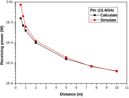
(28) 0.01. Pin @2.4GHz Calculate Simulate. Receiving power (W). 1E-3. 1E-4. 1E-5. 1E-6 0. 1. 2. 3. 4. 5. 6. 7. 8. 9. 10. 11. Distance (m). Figure 1-1-2 The calculated and simulated results of the received power varying with distances. Distance 0.5. 0.75. 1. 2. 5. 7.5. 10. (m) Calculated 1.58E-37.0362E-43.95786E-49.89465E-51.58314E-57.0362E-63.95786E-6 (Watt) Simulated 7.32E-3 2.03E-3. 6.13E-4. 1.23E-4. 1.914E-5. 6.72E-6. 4.10E-6. 0.6456. 0.8044. 0.8271. 1.047. 0.9653. (Watt) C/S value 0.204. 0.3466. Table 1.2 The calculated and simulated results of the received power varying with distances.. 26.
(29) Figure 1-1-3 Calculation of receiving power. 27.
(30) Chapter 2 Rectifier of a wireless microsensor. The received power of a wireless microsensor depends on the distance between the transmitter and receiver. Generally, the received power is about -10 ~ -20 dBm at the distance of 1 meter while the transmitting power is one watt. In order to efficiently use the input RF power for microsensor applications, the rectenna composed of an antenna and a rectifier is used to convert the RF power to DC voltage. In this research, we use two zero bias schottky diodes (HSMS-2850) to form a voltage doubler. The HSMS-2850 is designed and optimized for use in small signal applications. They are ideal for RFID and RF tag applications where primary (DC bias) power is not available. The zero bias schottky diode is modeled as Figure 1-2-1. The equivalent model includes the parasitic effect due to the device package. Table 2.1 shows the spice parameters for the HSMS-2850. These spice parameters are provides by Agilent manufacturer. Here, the advanced design system (ADS) software is used to simulate the RF circuit performance.. Figure 1-2-1 Equivalent model of HSMS 2850 28.
(31) Bv. Cj0. EG. IBV. IS. Units. V. pF. eV. A. A. 2850. 3.8. 0.18. 0.69. 3E-4. 3E-6. N. 1.06. RS. PB. Ω. V. 25. 0.35. PT. M. 2. 0.5. Table 2.1 Spice parameters for HSMS 2850. In the equivalent model, Rs is parasitic series resistance of the diode, the sum of the bondwire and leadframe resistance, the resistance of the bulk layer of silicon. RF energy coupled into Rs is lost as heat- it does not contribute to the rectified output of the diode. Cj is parasitic junction capacitance of the diode, controlled by the thickness of the epitaxial layer and the diameter of the schottky contact. Rj is the junction resistance of the diode, a function of the total current flowing through it. Rj =. 8.33 * 10−5 * n * (T + 273) I s + Ib. (2-1). Where n = ideality factor T = temperature I s = saturation current I b = externally applied bias current I s is a function of diode barrier height, and can range from picoamps for high barrier diodes to as much as 5 uA for very low barrier diodes. In general, very low barrier height diode (with high values of Is, suitable for zero bias applications) are realized on p-type silicon. Such diodes suffer from higher values of Rs than do the n-type. Besides, Lp is about 2 nH, Cp is 0.08 pF, Rs is 25 ohm, and Cj is about 0.18 pF. The most difficult part of the design of a rectified circuit is the input impedance matching network. The input 29.
(32) impedance of the voltage doubler at the frequency of 2.4 GHz as shown in Figure 1-2-2 is about 9.668 – j*113.449. Because the input impedance of the receiving antenna is designed as 50 ohm, the matching network must be designed between the rectifier and the antenna, the impedance matching is done from 50 ohm to 9.668 – j*113.449. The impedance matching circuit including an inductor of 7.535 nH and a resistance of 40.33 ohm is shown in Figure 1-2-3. Because the RF system is operated at the frequency of 2.4 GHz, the rectenna circuit is optimized at the operational frequency and shown in Figure 1-2-4. In the circuit, the two capacitances have the values of 100 pF, and the load resistance is 100 kOhm. Besides, the Smith Chart tool is used to match the receiver antenna and the rectifier presented as Figure 1-2-3. The return loss of the rectenna circuit is presented in Figure 1-2-5.. Figure 1-2-2 Impedance matching circuit of voltage doubler @ 2.4 GHz. 30.
(33) Figure 1-2-3 Matching circuit between receiver antenna and rectifier. Figure 1-2-4 The rectenna circuit @ 2.4 GHz. 31.
(34) Figure 1-2-5 Return loss of the rectenna circuit. From Figure 1-2-5, it can be noted that the rectenna circuit has the return loss of -55.107 dB at the frequency of 2.4 GHz and the impedance bandwidth of 0.62 GHz from the frequency of 2.105 GHz to 2.725 GHz. The transfer simulation of the rectenna circuit is developed in Figure 1-2-6. We use harmonic balance approach to simulate the transfer characteristics, and the first third order harmonic modes of the operational frequency of 2.4 GHz are considered. The RF input (Pin) simulated the receiving power from the antenna sweeps from -50 dBm to 30 dBm. Besides, the noise effect on all components is also considered in this simulation. The transfer curve of the rectenna circuit is shown in Figure 1-2-7. If the RF input power is -30, -20, -10 dBm, we can achieve a DC output voltage of 11.629 mV, 87.050 mV, and 415.183 mV. It can be noted that the transfer curve shows two regions of square law response and the linear law response. The boundary of the two regions is about at the input power of -15 dBm. The region above the boundary is the linear law response, and the region below the boundary has the square law response.. 32.
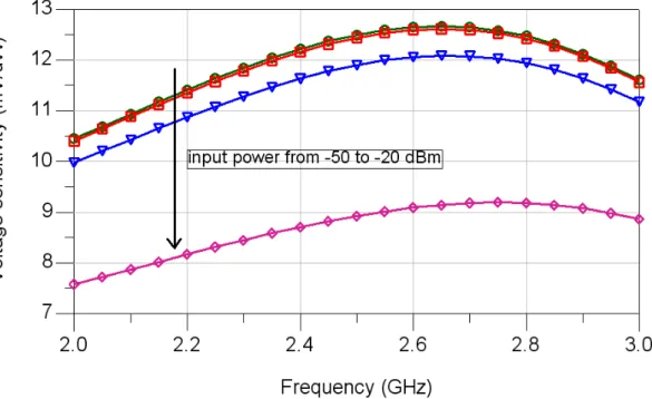
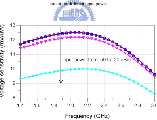
(35) In the RFID application, the square law region is the better operational region due to its large voltage sensitivity. The voltage sensitivity varying with frequency of the rectenna circuit for different input power is shown in Figure 1-2-8. The input power varies from -50 dBm to -20 dBm. It can be seen that the maximum voltage sensitivity occurs at the frequency of 2.65 GHz for the input power of -50 ~ -30 dBm and the maximum sensitivity for the input power of -20 dBm is at the frequency of 2.7 GHz. In order to compare with the rectifier with single schottky diode, we have also implemented the single diode rectenna circuit. The transfer cures of the rectenna circuits with single, double and triple schottky diodes are shown in Figure 1-2-9, and it can be noted that the single diode rectenna has larger output voltage than the double and triple diode ones below the input power of -30 dBm, but it has less output voltage than double and triple diode rectenna circuit above the input power of -30 dBm. This can be explanted by the series resistance and parasitic resistance of the rectenna circuit. Besides, the voltage sensitivity varying with frequency of the single diode rectenna circuit for different input power is presented in Figure 1-2-10. The maximum voltage sensitivity at the input power from -50 dBm to -30 dBm occurs at the frequency of 2.95 GHz higher than that of the double diode rectenna circuit, and the sensitivity decreases as the input power increases due to the operation from the square law response to the linear law response as shown in Figure 1-2-11.. 33.
(36) Figure 1-2-6 Transfer simulation of the rectenna circuit. Figure 1-2-7 Transfer curve of the rectenna circuit. 34.
(37) Figure 1-2-8 Voltage sensitivity varying with frequency of the rectenna circuit for different input power. Figure 1-2-9 Transfer curves of the rectenna circuit for single, double and triple schottky diodes 35.
(38) Figure 1-2-10 Voltage sensitivity varying with frequency of the single diode rectenna circuit for different input power. Figure 1-2-11 Voltage sensitivity varying with frequency of the triple diode rectenna circuit for different input power. 36.
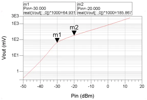
(39) In order to further improve the simulated exactness, we use microstrip lines to implement the matching circuit and also include the package influence of the HSMS-2862 by including capacitances and inductances. Because the vendor does not give us the zero-bias schottky diodes of HSMS-2850 yet, we use HSMS-2862 instead of HSMS-2850. The HSMS-2862 have been designed and optimized for use from 915 MHz to 5.8 GHz. It is ideal for RFID and RF tag applications. In small signal detector applications (Pin < -20 dBm ), this diode is used with DC bias at frequencies above 1.5 GHz. In larger signal power applications ( Pin > -20 dBm), it is used without bias at frequencies above 4 GHz. When DC bias is available, Schottky diode detector circuits can be used to create low cost RF and microwave receivers with a sensitivity of -55 dBm to -57 dBm. Figure 1-2-12 shows the configuration of the rectenna circuit whose matching network is made by microstrip line. The transfer curve of the rectenna circuit with the microstrip line is presented in Figure 1-2-13. The output voltage with the received RF power of -30 dBm and -20 dBm at the frequency of 2.4 GHz are about 64.932 mV and 185.867 mV, respectively. The photograph of the real rectenna circuit is shown in Figure 1-2- 14. We use chip resistance, chip capacitance and HSMS-2862 to implement the circuit, and the measured results of output voltage against transmission distance are shown in Figure 1-2- 15. From these, it can be noted that the measured output voltage is less than the predicted result due to the fabrication tolerance and the RF property of these passive chip devices. The RF input power of the transmitting antenna is 13 dBm which is the limitation of our equipments.. 37.
(40) Figure 1-2-12 Transfer simulation of the rectenna circuit with the microstrip line. Figure 1-2-13 Transfer curve of the rectenna circuit with the microstrip line. 38.
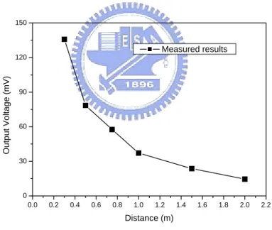
(41) 100kOhm. 100pF. HSMS2862. Figure 1-2- 14 Photograph of the real rectenna circuit for the frequency of 2.4 GHz. 150. Measured results. Output Voltage (mV). 120. 90. 60. 30. 0 0.0. 0.2. 0.4. 0.6. 0.8. 1.0. 1.2. 1.4. 1.6. 1.8. 2.0. 2.2. Distance (m). Figure 1-2- 15 Measured results of the output voltage against transmission distance. 39.
(42) Part II. Design and simulation of an uncooled microbolometer with low temperature CMOS-process compatibility. 40.
(43) Chapter 1 Introduction. 1.1 Characteristics of infrared. The range of infrared wavelengths is from 0.76 um to 1000 um. It can be divided into four groups which are near infrared (0.76 um~1.5 um), middle infrared (1.5 um~5.6 um), far infrared (5.6 um~25 um), and extra far infrared (25 um~1000 um). Crawford F.J. [1] presented the spectral dependence of radiation on temperature shown as Figure 2-1-1 Every object that is not at absolute zero emits and reflects electromagnetic radiation. The wavelength of the radiation is a function of the temperature of the object. Shorts wavelengths are emitted by higher temperatures and longer wavelengths are emitted by cooler objects. The short wavelengths between 0.45 um to 1um used by visible cameras are emitted by very hot sources, such as the sun or incandescent light bulbs. However, the longer infrared wavelengths between 3 and 14 um are emitted by objects at temperatures around 300 K or 25 oC.. Figure 2-1-1 Spectral dependence of radiation on temperature. 41.
(44) Radiation is either scattered or absorbed by gas molecules, rain, and snow as it propagates through the atmosphere. Figure 2-1-2 shows the atmospheric transmission characteristics from visible to 14 um. It can be noted that the two infrared transmission windows at 3 to 5 um and 8 to 12 um are the wavelengths encompassed by terrestrial temperatures. These transmission windows dictate the choice of wavelengths used in the infrared sensor design.. Figure 2-1-2 Atmospheric transmission characteristics 1.2 Infrared (IR) detector. Over the past several years, uncooled infrared (IR) radiation detectors have been rapidly developed into a large size of focal plane arrays (FPA). IR detectors have been an important technology for both military and civilian application, such as night vision, surveillance, detection of gas leakage, fire rescue operation, manufacturing quality control, early fire detection, and missile tracking, guidance, discrimination, and interception [2-5]. There are basically two types of IR detectors: photon and thermal detectors [6]. Traditionally, photon detectors are preferred primarily due to their superior 42.
(45) sensitivity. However, the photon detectors must be cooled to approximately the temperature of liquid nitrogen, with the cooling apparatus typically which is the most expensive component in a photon detector’s IR camera. Most thermal detectors, on the other hand, don’t need such an apparatus, and they are uncooled and comparatively inexpensive. In addition, the recent advances in micromachining technology have made it possible to fabricate highly sensitive thermal IR detectors. Hence it can decrease the cost of the system, offer improved reliability and mean-time-before failure (MTBF), instant operation, sensitivity in the spectral region of 8 um to 12 um. Conventional uncooled IR detectors, which have long been used for human image detection and temperature measurements, have a very small number of elements, sometimes only one. This is insufficient for tracking moving IR images; here, it is necessary to increase the number of elements and to integrate them into a two dimensional (2 D) array. Such an array sensor is called a focal plane array (FPA), or an array image sensor. Three different types of uncooled FPA have been developed. They are bolometer detectors [3, 7], thermopile detectors [8], and pyroelectric detectors [9-10]. Bolometers are generally easier to fabricate than pyroelectric detectors and have better responsibility than thermopiles [6]. The bolometer detectors are adopted in this dissertation.. 1.3 Micromachining technology with integrated circuits for micro-sensor applications. In recent years, microelectromechanical systems (MEMS) have emerged as a very promising field of researches and applications. There is a tendency towards developing a smart sensor which is a combination of sensors and integrated circuits (ICs) in the same chip. Practical implementation of smart sensors has still a lot of problems to be solved such as the difficulty in integrating different fabrication technologies. From the very beginning, integration of microelectromechanical systems (MEMS) with integrated circuits (ICs) was a major attraction of silicon micromachining. 43.
(46) technology. Practical implementation has not been easy. While the first pressure sensors reached the market in the 1960s, many first integration efforts failed, yielding the first practical, integrated pressure sensors in the 1980s [11]. The 1990s brought multiple product launches of integrated MEMS-IC devices, such as acceleration sensors, ink jet print heads, and display chips. In the current decade, integrated gyro sensors entered the market. All these efforts focused on integrating MEMS processes and IC processes on the same wafer. Incompatibilities forced long and expensive development cycles. Several approaches of process integration between IC and MEMS were developed over the past two decades. Generically, they classify into three categories as the following: (a) Integration of MEMS on Top of IC (b) Lateral (side-by-side) MEMS and IC integration (c) Vertical wafer-level MEMS-IC integration. ¾. Integration of MEMS on Top of IC The most straightforward method of integration is to build the MEMS device. directly on top of the CMOS wafers. This has the severe disadvantage of requiring strict process compatibility. MEMS structures are limited to those that can be surface micromachined within the CMOS thermal budget (<400 ◦C). It rules out LPCVD polysilicon and silicon fusion bonding, a staple for many MEMS devices. Another restriction is that the exposed materials, a low-temperature oxide and aluminum, limit the chemical means available for processing. ¾. Lateral (Side-by-Side) MEMS and IC Integration This approach overcomes some process incompatibilities between MEMS and. CMOS. This method fabricates any CMOS incompatible processes first and then can do both bulk and surface micromachining. ¾. Vertical Wafer-Level MEMS-IC Integration This approach bonds together two or more wafers. At least one wafer is MEMS. and at least one other is CMOS. Each is fabricated in a dedicated foundry. Vertical wafer level integration of circuits and MEMS has several advantages over integrating MEMS 44.
(47) and active circuitry at the process level: (1) It lacks the restriction of process compatibility. (2) It does not suffer the real estate penalty and inefficiency of lateral integration techniques. (3) Because the MEMS and CMOS are fabricated separately prior to integration, it affords the designer absolute flexibility in the choice of active circuit process options. High-density digital, mixed signal, high voltage (HV), BiCMOS, and RF can all be integrated using the same process steps. The example of the wafer-level MEMS and IC integration is shown in Figure 2-1-3 [11]. Two wafers are preprocessed to fabricate the bond metallization. The bonding recipe requires a precise bonding pressure and temperature profile. It is possible to create bonds which are purely structural, or which can also conduct signals between the MEMS and the CMOS, thus functioning as a part of the electrical circuit.. 45.
(48) Figure 2-1-3 Vertical wafer-level MEMS-IC integration. 1.4 Surface micromachining on top of IC for bolometer detector applications. Although the technology of vertical wafer-level MEMS-IC integration provides many advantages over MEMS on top of IC and lateral MEMS-IC integration, it may not be the best choice for the IRFPA applications, which require a large number of elements and are very susceptible to environmental thermal noise and electrical noise. In order to obtain the best device performance of IR detectors, the surface micromachining on top of IC is the promising candidate for infrared detector applications. Hence, a low-thermal budget (<400℃), CMOS-process compatible, surface micromachining process becomes more and more attractive, and it is widely applied to commercial products and consumer goods due to its benefit of easy integration with ICs. 46.
(49) In addition, a low temperature (<400℃) process makes MEMS sensors be able to fabricate directly on ICs as a post-process. This is a very convenient approach to integrate MEMS devices with driving and sensing circuits into a chip, and this integration can improve immunity against noise and increase sensing sensitivity. The primary structures of the surface micromachining are suspension structures such as cantilever beam, bridge, diaphragm, and membrane [12]-[15]. In these structures, flatness of a freestanding diaphragm or a cantilever beam is an important issue for optical applications which are like optical switches and micro-mirrors [15]. However, the flatness and long-legs of membranes are even more a challenge than other devices to design and fabricate for thermally isolated applications, especially as low cost uncooled IR (infrared) microbolometers [16], [17]. The IR microbolometers are radiation sensors with an infrared absorber. Under IR illumination, the temperature of the absorbing layer increases and then the resistivity of the sensitive material changes. In order to acquire a microbolometer with high responsivity, the thermally isolated structure of the device is vital to ensure a maximum increase of temperature due to the absorption of IR radiation [16]. The most important part of the whole microbolometer is the suspension membrane serving as a structural layer on which the sensing material and the signal metal lines are located. Besides, regarding thermal isolation of the microbolometer, many microfabrication approaches have been presented to reduce the thermal losses and thermal mass of the membranes of the microbolometer structures. These approaches contain the use of low thermal conductivity materials and thermally isolated structures obtained by surface or bulk micromachining techniques [17]. In order to integrate easily with CMOS sensing circuits, the surface micromachining technique is preferable due to its small feature size and CMOS compatible processes. However, in the surface micromachining technique, the sticking effect and residual stress play an important role in determining whether the 47.
(50) microstructures are suspended or collapse during the release process. In general, the released microstructures are apt to be attached to the underlying layers. There have been many studies about sticking effect and residual stress with regard to the cantilevered beam structures by developing several different models [18]-[19]. However, no research has been done on the influence of the anchor profile of the membrane microstructure with residual stress. In addition, during the release process, drying of the delicate microstructures is another important issue for whether the device is successful or failure. Many release methods have been presented and compared [20]. To date, most drying methods of release apply CO2 supercritical point to overcome the sticking effect, but this method leads to low throughput, high cost and expensive apparatus. In this dissertation, we used hot plate to dry the release-etch microstructure to substitute for CO2 supercritical point method. Although Takeshi [21] described the effects of elevated temperature treatments in microstructure release procedures, these effects were only been investigated for cantilever.. 1.5 In our research. We first develop the test microbolometer structure from two aspects including structural design and material selection to obtain high thermal isolation structures. Then, the structure fabrication has been developed to reach the aims of lower processing cost, higher fabricating reliability, and compatible with CMOS processes. The design of the test microstructure by controlling the anchor profile containing sidewall conformal factor (SCF) and sidewall angle is investigated. In addition, the temperature effect during release procedures for single membrane and membrane array is also discussed.. 48.
數據
+7
相關文件
了⼀一個方案,用以尋找滿足 Calabi 方程的空 間,這些空間現在通稱為 Calabi-Yau 空間。.
好了既然 Z[x] 中的 ideal 不一定是 principle ideal 那麼我們就不能學 Proposition 7.2.11 的方法得到 Z[x] 中的 irreducible element 就是 prime element 了..
Wang, Solving pseudomonotone variational inequalities and pseudocon- vex optimization problems using the projection neural network, IEEE Transactions on Neural Networks 17
volume suppressed mass: (TeV) 2 /M P ∼ 10 −4 eV → mm range can be experimentally tested for any number of extra dimensions - Light U(1) gauge bosons: no derivative couplings. =>
The spontaneous breaking of chiral symmetry does not allow the chiral magnetic current to
Define instead the imaginary.. potential, magnetic field, lattice…) Dirac-BdG Hamiltonian:. with small, and matrix
• Formation of massive primordial stars as origin of objects in the early universe. • Supernova explosions might be visible to the most
* School Survey 2017.. 1) Separate examination papers for the compulsory part of the two strands, with common questions set in Papers 1A & 1B for the common topics in
