Chapter 1 Introduction
1.1 General Introduction
“There`s plenty of room at the bottom”, famous physic scholar Richard Feynman announced at the annual meeting of the American Physical Society at the California Institute of Technology. Until today many researches agree his viewpoint. Feynman imagined a new physical world of ultra-small volumes and highlighted some difficulties that researchers might encounter when visiting it. A new word comes out `nano`.
Nanotechnology is provided to many aspects when the dimension is lower than 100nm scale, many interesting phenomena dominate in this scale. The improvements in lithography have resulted in the continued reduction of line widths to well below 1 micron. As the different lithographic methods approach to their limits, the conventional lithographic methods have to be replaced instead of the new developing methods.
As the progress of the higher density of modern semiconductor device, devices has to become scaled down to smaller sizes to the nano-regime, and beside with the reduction of the size, the problems such as quantum mechanism dominates in the nano-scale. Lots of phenomena arise and the classical physics fail in the explanation. Therefore, the quantum mechanics arises.
Alternative manufacturing methods, materials, device structures, and architectures are required. In this regime, the approach of fabricating nanoelectronic devices and interconnects using a combination of molecular and nanostructured materials with existing and emerging processing technologies promises to allow the continued miniaturization and
enhancement in performance for the next generation of memory and logic chips.
The most important step is to develop applications that leverage the unique aspects of the nanoscale system .Many new developed techniques (especially nanobiotechnology) are still in the new stage, requiring incubation for application and assay development.
Figure 1.1 displays the progress of nanotechnology .
This figure clearly indicates the technical complexity for various applications.The suggestion of the this figure is beneficial for us to develop the next generation technology.
1.2 Top-Down Nanotechnology
Small patterns need to be achieved from various lithographic methods.[1] The lithographic techniques were used to define patterns in a electronic chip associated with functional influence. The semiconductor roadmap of the line-width for the memory device illustrated a tendency as shown in Figure 1.2.
The light source is the key factor to define the line-width of the exposed device. The progress of the light source exceed from G-line (436 nm), I-line (365 nm), now the subsequent light source is 193 and 157nm. Figure 1.2 lists the semiconductor industry roadmap in the years 1999–2005 and the predictions for subsequent years to 2014.[2]
The shorter wavelength is needed to increase the resolution. According to Rayleigh`s formula[3],the resolution W and the depth of the focus are given in the following equation:
W=k1λ/NA , DOF=k2λ/(NA)2 Where theλ is the wavelength of the light
source, NA is the numerical aperture and the k1, k2 arethe constants.
Figure 1.2 Semiconductor roadmap of the line-width for the memory device
The higher the resolution, the smaller pattern is expected. With the reduction of theλ,the resolution W will be higher, but the DOF[4] means a range of focus errors which keeps the resist profile of a given feature within specifications over a specified exposure range. To achieve the higher resolution, the DOF should be in the ideal range and avoid the misfit problem caused by the out of the focus.
The optical lithography techniques will close to the limits of resolution, the bottleneck of the patterns will be encountered in the 10 years. The physical limit, 5–20-nm line widths will be a barrier difficult to be overcome.
The 65–90 nm range needs some techniques including liquid immersion lithography (LIL)[5]—Despite the invention of some impressive techniques that increase process resolution—such as the use of phase shift masks (PSM),[6] off-axis illumination (OAI)[7]and optical proximity correction (OPC). [8] Over 65-90nm, below the 65nm line-width, the new-developed techniques like extreme ultraviolet (EUV) lithography,[9] electron beam projection lithography (EPL),[10] proximity X-ray lithography (PXL),[11] electron beam direct writing (EBDW) [12]and ion beam projection lithography (IPL)[13] can be used to fabricate tiny patterns in semiconductor devices. The “next-generation ” lithography is indeed needed to be applied in modern semiconductor industry to satisfy the fabrication of tiny device in higher density of modern electronic device.
The top-down method including EBDW, EUV, EPL, PXL, and IPL and soft lithography (i.e. nanoimprint). Figure 1.3 displays the concept of
soft lithography[14] , which based on the mechanical force acted on the soft photoresist film. When the contact area is heated by the exposed light through transparent PDMS and the pattern formed because of the force. The continued pressurization of the PDMS module made the pattern appeared.
Figure 1.3 The concept of soft lithography (source: Physics World 11 (1998) 31–36).
The soft lithography is based on the use of elastomeric polymers to transfer a pattern from a master to a large number of copies having single-layer structures.The fabrication process of soft lithography including microcontact printing (CP),[15] microtransfer molding (TM),[16] replica molding (REM),[17] micromolding in capillaries (MIMIC),[18] and solvent-assisted micromolding (SAMIM),[19] and PDMS
Poly(dimethylsiloxane) molds.[20] The pattern in nano-scale is usually defined by the use of the microcontact printing for SAM on the substrate. The advantage of the soft lithography including easy process and simple equipment without clean room, but the shortage is the low yield and ineffective for transferring multi-layer into precise alignment. Based on the mechanical embossing principle, the resolution limits of light exposure can be overcomed when the nanoimprinting technique is used to semiconductor industry to avoid the shortage caused by light diffraction or e-beam scattering in other conventional techniques.
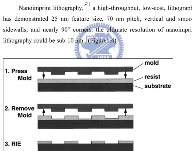
Nanoimprint lithography,[21] a high-throughput, low-cost, lithography has demonstrated 25 nm feature size, 70 nm pitch, vertical and smooth sidewalls, and nearly 90° corners. the ultimate resolution of nanoimprint lithography could be sub-10 nm . (Figure1.4)
Figure 1.4 Schematic diagram of nanoimprint lithography process: (1) imprinting usinga mold to create a thickness contrast in a resist, (2) mold removal, and (3) pattern transfer using anisotropic etching to remove residue resist in the compressed areas.
Nanoimprint lithography[22]has two basic steps : the first is the imprint step in which a mold with nanostructures on its surface is pressed into a thin resist cast on a substrate, followed by removal of the mold. The second step is the pattern transfer where an anisotropic etching process, such as reactive ion etching (RIE), is used to remove the residual resist in the compressed area. This step transfers the thickness contrast pattern into the entire resist. During the imprint step, the resist is heated to a temperature above its glass transition temperature, and the patterns are transferred into the desired position.
With further development, imprint lithography can become the technology for manufacturing nanostructures, and can have a significant impact in many areas such as integrated circuits, biology, and chemistry .It also avoids the diffraction effects during optical lithography, proximity effects during EBDW and EPL and difficulties in mask fabrication for X-ray and EUV lithography.
1.3 Bottom-Up Nanotechnology
Two general methods available for producing nanosized materials are shown in Figure 1.5. The top-down approach starts in a bulk material and then breaks it into smaller pieces using mechanical, chemical, or other forms of energy.
On the contrary, the bottom-up methods is to synthesize the material from atomic or molecular species through chemical reactions that allow the precursor particles to grow in size. The bottom-up methods can be used for nanostructure. The atoms and molecules are assembled into the smallest nanostructures (dimensions of typically 2 to 10 nm) by carefully controlled
chemical reactions.
Self-assembly of atoms and molecules into nanostructures can be classified as a type of bottom-up method. The formation of self-assembled monolayers (SAMs), that are produced when a substance spontaneously forms a molecular monolayer on a surface, could be successfully combined with standard lithographical methods to achieve large-scale and better controlled structure. Biologically inspired self-assembly holds great promise in nanostructuring. For instance, it can be used in the formation of peptide nanotubes by self-assembly of cylindrical octapeptides, tubes that function as ion channels. (Figure1.6) [23,24,25]
Figure 1.5 Methods available for producing nanosized materials
Figure 1.6 Peptide nanotubes by
The fabrication of carbon nanotubes (CNT) and quantum dots have been proposed for studying the physics in one-dimensional solids as well as being used in various nanoscale devices.[26] They can be self-assembled into hierarchical structures with controlled nanotube orientation .[27]
Nanocrystals including organic biological compounds, metal, semiconductor and inorganic oxide can be fabricated through the chemical self-assembly methods. All the methods conclude selective attachments of molecules on specific surface [e.g., thiol (–SH) end groups] can be used to be 1D, 2D, and 3D self-assembled nanostructures.
1.4 Comparison of top-down and button-up methods
Two distinct strategies have been used to explore the nanometer
domain (i.e., 1–100nm)—‘bottom-up’ and ‘top-down’. [28] For the former,
nanoscale materials are assembled from smaller molecular and atomic components. Here, nanomaterials, such as quantum dots and nanobars, can be synthesized or designed layer by layer, blending techniques from chemical engineering and material science. The innovation lies in precise control of the material’s size and results in optical and electronic properties. Dendrimer and liposome technologies are derived from well-established bottom-up synthetic techniques, built to scale using chemistry and self-assembling lipids, respectively.
The top-down development path is guided to the nanoscale by fabrication tools from the electronics industry, where techniques of lithography, embossing and contact printing are used to create micron-scale array elements and fluidic pathways. Top-down methods start with patterns made on a large scale and reduce its lateral dimensions before forming
nanostructures. These micron-sized components can be used to manipulate submicron (nanometer) amounts of material.
Ultimately,nanotechnology-based products will require a convergence of the two approaches for practical use, both to engineer the nanoscale device and to interface with the outside world. The bottom-up approach permits control of the chemical and structural architecture; however, manual assembly of individual nanometer-sized components is clearly prohibitive in time and cost. Top-down technologies provide a progressive interface from the real world (meters, millimeters, microns) to control at the nanometer scale. Table 1.1 summarizes the methods . [29]
1.5 Motivation
Nanotechnology is a dominate phrase talked by people. Building blocks like atoms and molecules integrated into tiny structure or devices . Nowadays, If it is possible to examine how biological systems perform molecular processes and signaling in the living body by a clear way. One approach to nanotechnology may be feasible.
According to the report,[30] it is effective to detect DNA molecules with silicon nanowire. The complete DNA (deoxyribonucleic acid) consists of two strands of DNA with specific sequence nucleotides, which binding together to form a stable structure.
Radiolabeling and fluorescence labeling techniques are the most used methods for DNA sensing. However, the methods need long half-life for radioisotopes such as 32P .Conventional methods of DNA detection spend a lot of time and money. In order to detect diseases such as cancer, diabetes, and hypertension, many research groups detect DNA through electrical signal corresponding to the DNA sequence. The Lieber group has proposed the use of silicon nanowires as powerful sensors for biological, chemical, and PH meter.[31] When the binding of specific DNA molecules on the silicon nanowire, the distribution of charge changes that affect the conductivity. When an FET device channel width is on the nano-scale, the device can be considered to be a nanowire sensor.
Togetger with the research illustrated above, we plan to try to bind bio-molecule with complex structure such as protein. Rapid, multiplexed detection of protein with high selectivity and sensitivity is necessary. This goal has not been attained with any existing method, Recently, there has been an increasing demand to find simple and rapid methods for the
detection of specific protein, which can also be used easily in non-specialized laboratories. The detection of specific protein is critical importance because protein mutation can induce a couple of diseases. The traditional techniques for protein identification are enzyme-linked immunosorbent assay, [32] fluorescence immunoassays,[33] and western blot .[34] The drawback of above methods is time-consuming, tedious labeling process and poor sensitivity.
Solid state electronic device such as nanowires[35] and nanogaps[36] nanoparticles,[37] microcantilevers,[38] and carbon nanotubes[39] are provided as the tool for the detection of protein. The advantage of them are high sensitivity and low-cost .The attachment of protein must be strong and high selective . Based on the strong chemical-bonding between gold and thiol, the gold silicide nanowire is provided as the suitable platform to sensing the protein such as streptavidin.
Gold silicide nanowires were defined by electron beam lithography (EBL) and fabricated using a standard semiconductor process. After thermal evaporation of gold, the following anneal process at temperature ranging from 400oC to 650oC is used to form gold silicide. The surfaces of gold silicide nanowires were then modified to allow the attachment of bio-molecule. The conductance of the nanowires is lower when streptavidin attached. These findings highlight the potential of this system for use as a protein sensor and for its integration into the processes used for the mass production of semiconductors.
Chapter 2 Review of Silicon Nanowires
2.1 Bottom-up Method for Nanowires
Nanoscale-building blocks require with precisely controlled and tunable chemical composition, structure, size and morphology. It is critical to develop and explore the limits of functional devices based on these building blocks. The development of architectures enables high-density integration with predictable function, and hierarchical assembly methods that organize building blocks into these architectures. bottom-up approach in which functional device elements and element arrays have been assembled from solution through the use of electronically well-defined semiconductor nanowire building blocks.[1]
The crossed nanowire p-n junctions and junction arrays in Figure 2.1 can be assembled with controllable electrical characteristics. Integrated nanoscale field-effect transistor arrays can be fabricated and with nanowires as both the conducting channel and gate electrode. Nanowire junction arrays can be modified as OR, AND, and NOR logic-gate structures. Figure 2.2 with substantial gain has been used to implement basic computation.
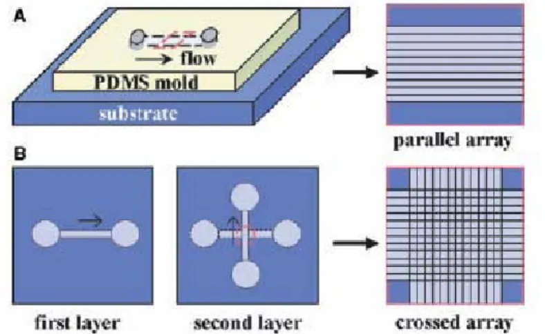
The assembly of these nanowires onto devices by Lieber and co-workers have developed[2] fluidic alignment with surface-patterning techniques to accomplish the large-scale hierarchical organization of nanowire arrays for integrated nanosystems.Fluidic channel structure was illustrated in Figure 2.3 that nanowires could be assembled into parallel arrays with controlled average separation; poly(dimethylsiloxane) (PDMS) mold was applied that the fluidic channel was fabricated to control the periodicity. Layer-by-layer assembly to be aligned within a area contains
complex arrays of crossed nanowires.
Figure 2.1 Diagrams of crossed
nanowire p-n junctions and junction arrays
Figure 2.2 Diagrams of OR, AND, and NOR logic-gate structures
The assembly of functional nanoscale devices from indium phosphide nanowires shows the electric-field-directed assembly.[3] It can be used to create highly integrated device arrays from nanowire building block. The electric fields to align and position individual nanowires into parallel and crossed arrays (Figure 2.4). The potential of this approach was demonstrated by aligning many nanowires between parallel electrodes.
2.2 Top-down Method for Nanowires
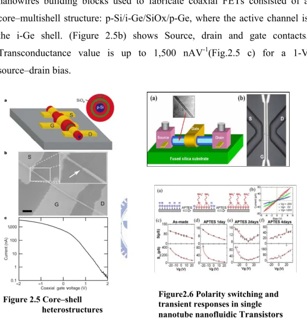
Semiconductor heterostructures with modulated composition and/or doping enable passivation of interfaces and the generation of devices with diverse functions. Core–shell heterostructures formed by the growth of crystalline overlayers on nanocrystals offer enhanced emission efficiency.[4] Axial heterostructures have also been formed by a one-dimensional modulation of nanowire composition and doping.[5] In Figure 2.5a,[6] the
nanowires building blocks used to fabricate coaxial FETs consisted of a core–multishell structure: p-Si/i-Ge/SiOx/p-Ge, where the active channel is the i-Ge shell. (Figure 2.5b) shows Source, drain and gate contacts. Transconductance value is up to 1,500 nAV-1(Fig.2.5 c) for a 1-V source–drain bias.
The integration of inorganic nanotubes into metal-oxide-solution field effect transistors (FETs) which exhibit polarity switching and transient responses.[7] Surface functionalization can switch the nanofluidic transistors from p-type to ambipolar and n-type field effect transistors. Figure 2.6 illustrates the device and it`s electrical signal with modifying molecule.
Figure 2.5 Core–shell heterostructures
Figure2.6 Polarity switching and transient responses in single nanotube nanofluidic Transistors
2.3 Application for the Protein Detection
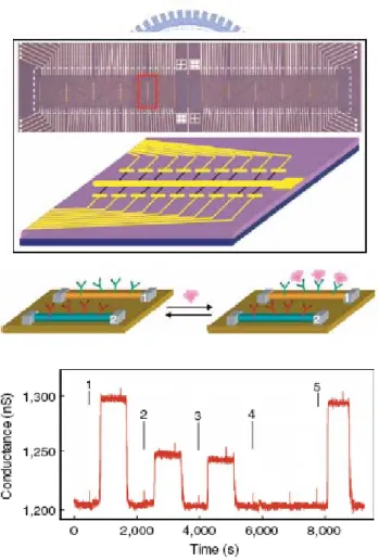
Multiplexed electrical detection of cancer markers using silicon-nanowire field-effect device[8] in which distinct nanowires and surface receptors are incorporated into arrays. Protein markers were routinely detected at femtomolar concentrations with high selectivity. The capability for multiplexed real-time monitoring of protein markers and telomerase activity with high sensitivity and selectivity in clinically relevant samples opens up substantial possibilities for diagnosis and treatment of cancer and other complex diseases.
Figure 2.7 Multiplexed electrical detection of cancer markers with nanowire sensor arrays.
Chapter 3 Experimental Section
To test the feasibility of gold silicide, the poly-silicon thin film was deposited using LPCVD on the p-type silicon wafer. Beside with gold film coating, the annealing transformed the poly-silicon to the gold silicide. After the removal of gold with immersing in the aqua regia, the binding of bio- molecule was accomplished and the fluorescent experiment was applied.
The methods for the fabrication of silicon nanowires include bottom-up and top-down, mentioned in the previous chapter. This chapter discusses the fabrication of nanowires and the bridge resistor test structure contains 4-probe measurement. The E-beam direct writing was used to define the nanoscale pattern, the nanowire with width below 80nm can be achieved. The succeeding etching process defines the poly-silicon nanowire definitely. The gold silicide will be formed through the annealing process range under appropriate temperature. After the removal of un-reacted gold,
the nanowire was formed. These fabrication processes all employed
commercial semiconductor equipment located in the National Nano Device Laboratories.
3.1 General Introduction
All reagents and solvents were of reagent-grade quality, purchased commercially, and used without further purification, unless otherwise noted. The experimental reagents included:
Bovine serum albumin {BSA; for molecular biology, powder}
Bovine serum albumin was prepared by approximately 50% of the total protein in serum. It is an on-acetylated protein suitable as a blocking agent.
This chemical had very unpleasant smell and must be handled in the hood. Any spoil must be cleaned with active charcoal immediately
(+)-Biotin hydrazide {C10H18N4O2S; ~98%; Sigma}
This reagent was for labeling surface functional groups and biologically active molecules such as antibodies, lectins, sugars, nucleic acids or molecules with free carboxylic or keto groups. Typically used for coupling to glycoproteins through the carbohydrate by hydrazone formation. Stored in 4oC.
Phosphate-buffered saline tablets {PBS, 1X; CALBIOCHEM}
PBS, a biological buffer solution, was used to increase the selectivity of the DNA chips by washing away any non-hybridized nucleic acids. This chemical is dissolved in one liter ddH2O to yield 10 mM phosphate buffer,
pH 7.4, 140 mM NaCl, 3 mM KCl.
Sodium phosphate dibasic dihydrate {NaH2PO4; ≥99.5%;
Riedel-deHaën}
Sodium phosphate solution was widely used biological buffer. This chemical was also an ingredient of PBS.
Streptavidin−FITC from Streptomyces avidinii {essentially salt-free, lyophilized powder,≥ 5 units/ mg protein; Sigma}
This protein showed high affinity to biotin. The powder needed to dissolve in the PBS prior to to use. It must be stored at -20℃.
Sulfosuccinimidyl 4-[N-maleimidomethyl]-cyclohexane-1-carboxylate {sulfoSMCC;C16H17N2NaO9S; Sigma}
SulfoSMCC was water soluble, non-cleavable and membrane impermeable crosslinker. It contains an amine-reactive N-hydroxysuccinimide (NHS ester) and a sulfhydryl-reactive maleimide group.
3.2 Fabrication Process
Single-crystalline p-type <100> silicon wafers were used through all
the experiments. Four major steps are used for fabrication lists as (1) polycrystalline silicon nanowires, (2) deposition of the gold thin film and formation of gold silicide, (3) the process includes the attachment of the linker layer on the gold silicide and the binding of biotin and streptavidin and (4) detection of each bio-molecule in sequences.
3.2.1 Fabrication of Polycrystalline Silicon Nanowires (PSNWs)
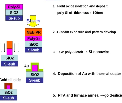
Figure 3.1displays the process for the fabrication of silicide nanowire.
Poly-Si SiO2 Si-sub Poly-Si SiO2 Si-sub E-beam NEB PR SiO2 Si-sub SiO2 Si-sub Au SiO2 Si-sub Gold-silicide
1. Field oxide isolation and deposit poly-Si of thickness = 100nm
2. E-beam exposure and pattern develop
3. TCP poly-Si etch → Si nonowire
4. Deposition of Au with thermal coater
5. RTA and furnace anneal →gold-silicide
Single-crystalline p-type <100> silicon wafers were cleaned through standard RCA cleaning. The silicon dioxide film (5000 Ao) was grown in thermal oxidization furnace as the isolation layer. The succeeding deposition of poysilicon layer (100 nm) is achieved in low pressure CVD. The electron beam resist NEB 22-A was spin-coated using a TEL CLEAN TRACK MK-8.
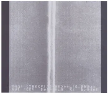
Leica WePrint 200 e-beam writer was used to pattern nanowires of various widths and contact pads. Tetramethyl ammonium hydroxide (TMAH) solution was used for development. After the tuning of appropriate dose, the desired shape of photoresist was obtained came out. The nanowire pattern was shown in Figure 3.2.
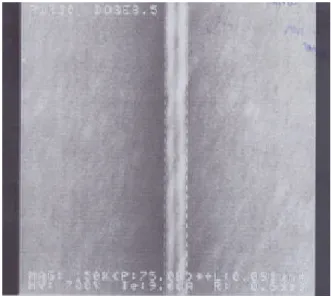
The polysilicon layer was etched using a TCP (LAM TCP 9400SE). Then the wafer was treated with thermal ozone (FUSION OZONE ASHER) and dipped the wafer in H2O2/H2SO4 (3:1) solution for 10 min. Finallly, the 80-nm polysilicon nanowires was shown in Figure 3.3.
Figure 3.2 The inline SEM image of developed 80nm nanowire
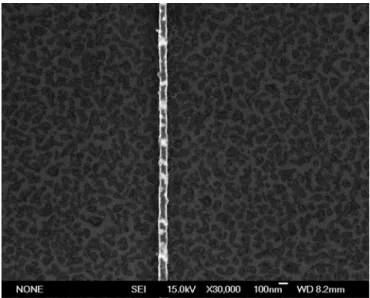
The nanowires can shrink to 70nm through SC1 <NH
4OH/H22/H2O
(0.25:1:5)> solution and the morphology is illustrated in Fig 3.4. [1]
Figure 3.3 The inline SEM image of 80nm poly-Si nanowire
Figure 3.4 The inline SEM image of SC1-etching 70nm poly-Si nanowire
3.2.2 Deposition of a Gold Film and the Formation of the Gold
Gold thin film (50nm) was deposited on the polysilicon nanowires using thermal coater and then annealed at temperature ranged from 400oC to 500oC including two methods of annealing – RTA and furnace. The gold silicide was formed under above process. The resulting wafers were immersed in HNO3/HCl solution (1:3) at 75 °C to remove the un-reacted gold. Figure 3.5 shows the morphology of the nanowire.
3.2.3 Attachment of the Protein for the Linkage of Silicide Nanowire
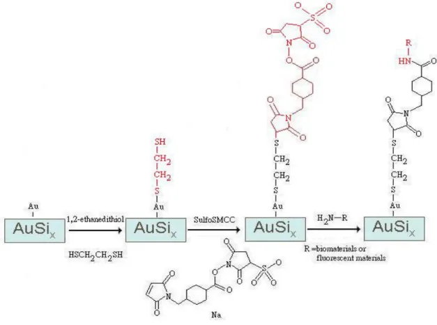
Figure 3.6 illustrates the process of immobilization of biomelecules
onto the gold silicide. All the experiments here were operated under room temperature. We sequentially washed the gold-silicide nanowires with ddH2O, ethanol, and acetone in order. Then, the nanowire was immersed in
the 5% 1,2-ethanedithiol of DMF solution for 30 minutes.
After sequential DMF, ethanol, and ddH2O washing, the sample was
again immersed in the 0.1 % sulfoSMCC solution for one hour. SulfoSMCC
was dissolved in the 100 mM sodium phosphate buffer of pH 6.8. The
sample also washed with sodium phosphate buffer after immersion. The hydrazide-biotin was dissolve in the DMF at 50 mM and diluted to 5
mM with 100 mM sodium phosphate, pH 7.5.
The nanowire was immersed in the biotin solution for 2 hours and also washed with sodium phosphate buffer to removal unbound biotin. The final step was to immerse the biotin-assembled nanowire in the 0.1 % FITC-streptavidin solution for 2 hours. FITC-streptavidin was dissolve in the PBS and diluted with the mixture of 10 mM pH 7.2 sodium phosphate buffer, 0.05 % NaN3, 0.15 M NaCl, and 0.1 % Tween 20.
Figure 3.6: The process of immobilization of biomelecules onto the gold silicide. R represents rhodamine or biotin.
3.2.4 Protein Detection
Based on the suggestion of reports,[2] [3] solid devices such as nanowire or nanogap can be used to detect biomolecule. At first the biomolecule such as biotin and streptavidin bind to the nanowire, the attachment of biomolecule will affect the charge distribution or theelectric field. Based on these effects, the resulted change of electrical property can be expected. The resulted electrical characteristics can be changed. Figure 3.7 displays the the sensing procedures for protein. The protein will bind on the nanowire and the resulted drop of sheet resistance is expected that will prove the sensing of the protein.
Chapter 4 Results and Discussion
Polysilicon and gold silicide on silicon wafers have been prepared in this study. At first we characterize the electrical behavior of the poly-Si nanowire by using an HP 4156A semiconductor parameter analyzer, and then characterize the gold silicide. We can understand the difference of them by means of the signal comparison.
The noise level of the electrical analyzer was measured to be ca. 50 fA (Fig 4.1) We can control the noise level to such low level for ensuring the reliability of characterization.
4.1 Physical and Electrical properties of Silicide film
After annealing the film, the silicide is formed on the surface. Figure 4.2 is the SEM picture for the gold silicide. Table 4.1 lists the
27
the poor uniformity of the gold silicide, the sheet resistance will be higher than furnace. In the Furnace, annealing time for 1 hour is used and the formation extent of gold silicide is higher than RTA method. Therefore, the sheet resistance is lower than RTA (in Figure 4.3). We adopt the furnace annealing technique based on the results of sheet resistance measurement.
Table 4.1 Comparison of poly-silicon and gold silicide film in resistivity Temperature resistivity (Ω- cm) 350 o C 103.822 400 o C 85.320 500 o C 9.682 600 o C 0.116 RTA 650 o C 0.114 400 o C 0.110 500 o C 0.090 method Furnace 600 o C 0.27
Figure 4.2 SEM picture of gold –silicide o the film
Figure 4.3 Comparison of RTA and furnace in electrical characteristics
4.2 Description of Bridge-resistor Structure
Figure 4.4 displays the Bridge-resistor structure [1]of gold silicide nanowire. It constitutes of four pads and three nanowire. The length of nanowire is 100μm and the width of nanowire ranges from 80nm to 200nm. Figure 4.5 displays the measured procedure for the conductance.
Figure 4.4 Bridge-resistor structure
Figure 4.5 Illustration for electrical measurement
Conductance = I
/ (V
-V
)
29
4.3 The Electrical properties of Polysilicon Nanowires
The electrical characteristics of polysilicon nanowire (80 nm width and 100 μm length) is shown in Figure 4.6. We determine the approximate conductance of the polysilicon nanowire to be 4 pS. Figure 4.6 determines the conductance at various widths. The conductance of poly-Si nanowire does not change too much with the reduction of width. The conductance of polysilicon nanowire is shown in Figure 4.7. The conductance of polysilicon is at the pS-scale ranging from 2 to 5 pS. The ideal conductance available from the literature is also in the same range of reports. [2]
Figure 4.7 Diagram of the conductance at various widths
4.4-1 The Physical and Electrical Properties
of Gold Silicide Nanowires
The silicide nanowire was accomplished after annealing at high temperature. The eutectic point of gold-silicon is 363oC upon the phase diagram.[3] (Figure 4.8) The gold silicide will form at temperature higher than eutectic point.[4]
The annealing temperature at 400, 500, 600 and 650oC transforms poly-Si to gold silicde.
31
Figure 4.9 shows the SEM picture of gold silicide nanowire.
Figure 4.10a-Figure 4.10e illustrates the conductance versus width at various temperatures. In Figure 4.10a, there is no obvious change of conductance because of the lower temperature than eutectic point (363oC). In Figure 4.10b –Figure 4.10e, the change of conductance is obvious at higher temperatures. After annealing temperature higher than 363oC, the sheet resistance will drop because of the low resistivity of gold silicide. Many factors affect the resistance of nanowire including of gold silicide uniformity, phase (constitution, structure) [5]of gold silicide, geometry effect (seen in Chapter 4.4-2.), narrow width effect[6]and narrow width edge effect.[7] Each factor competes and dominates depending on the condition.
Figure 4.10b –Fig 4.10c show the conductance versus width. The conductance will increase with the reduction of wire width as annealing
Figure 4.9 400oC Furnace for 1h At 80nm width
at 400oC and 500oC.
From SEM pictures, the gold silicide is the island-like (Figure 4.11a ,b ) distribution and it forms much barrier between poly-Si and gold silicide. Based on the narrow width effect, [6] the islands will decrease the conductance, and the phenomenon will dominate under small width. Figure 4.10b-Figure 4.10c show the tendency that the conductance will increase when the width of nanowire decreases. This phenomenon is different from that in Figure 4.10d and Figure 4.10e.
Under higher temperature such as 600oC and 650oC, the phase of gold silicide transformes to another phase which contained lower resistivity .[8] Figure 4.11c and Figure 4.11d display the SEM pictures of nanowires in 600oC and 650oC, respectively. The ratio of silicide is enhanced in the edge area, so the narrow width edge effect [7] and geometry effect will dominate the mechanism.
33
Figure 4.10c Conductance versus width at 500oC furnace Figure 4.11b Furnace 500oC - 200nm
Figure 4.11a SEM image of furnace at 400oC and 200nm width
Figure 4.10d Conductance versus width at 600oC
furnace
Figure 4.10b Conductance versus width at 400oC furnace
Figure 4.11c SEM image of furnace at 600oC and 200nm width
4.4-2 Geometry Effect:
The conductance will change with the variation of nanowire`s width. When the gold is thermally coating on the poly-Si, the succeeding annealing will transform the poly-Si to the gold silicide. The gold silicide formed on the nanowire is uniform and gold silicide thickness is about 10nm. Based on the observation (Figure 4.12a –Figure 4.12d), the ratio of poly-Si to gold silicide will increase with the reduction of width. For the higher ratio of gold silicide at smaller width, the sheet resistance will become smaller.
Figure 4.11d SEM image of furnace at 650oC
and 200nm width
Figure 4.12a Width=80nm Fig 4.12b Width=100nm
Figure 4.10e Conductance versus width diagram at 650oC furnace
35
4.4-3 The Effect of Gold Thickness to the Silicilation
The thickness of gold thin film can affect the density of gold silicide [9]. With increasing the gold layer thickness, the nucleation density of the Au-Si island is expected to decrease with increasing grain size, as illustrated in Figures 4.13a,b and Figures 4.14 a,b. [10]
The decrease in the number density of the gold silicide with increasing the gold thickness can be related to the decreasing nucleation density of the Au-Si islands. Thus the join of poly-Si and gold silicide will be enhanced with the thinner gold film. Hence the conductive path through poly-Si and silicide will be more. Figure 4.15a and Figure 4.15b display the distribution of silicide on the nanowire.
This phenomenon will enhance the conductivity of nanowire that the conductance of nanowire will be higher. Figure 4.16 displays the comparison of conductance at various thicknesses of gold thin film. In the smaller width (Figure 4.17), the difference of conductance will be
Figure 4.12c Width=120nm , gold silicide =10nm,
The coverage of gold silicide =25 %
Figure 4.12d Width=200nm , gold silicide =10nm, The coverage of gold silicide =19 %
enhanced with the more islands-like structure of silicide existing. The barrier between poly-Si and gold silicide is significant for smaller width. Thus, the resistance will increase effectively.
Figure 4.13a Formation of gold silicide
at 50nm gold thickness Figure 4.13 b Formation of gold silicide at 50nm gold thickness
Figure 4.15a
Figure 4.14b Formation of gold silicide at 10nm gold thickness
Figure 4.15b SEM image of gold silicide nanowire at 50nm thick gold
Figure 4.15a SEM image of gold silicide nanowire at 10nm thick gold
Figure 4.14a Formation of gold silicide at 10nm gold thickness
37
Figure 4.16 Sheet resistances at various thicknesses
4.5 Comparison of Poly-Silicon and Gold Siliscide Nanowire
As discussed in the previous section, poly-Si has much higher resistance than gold silicide whether in film or nanowire. The gold silicide nanowires used were prepared through the furnace process at different temperatures to attain the lower resistance as for biomolecule sensing. After annealing at 400oC, 500oC, 600oC and 650oC, the gold film separated into isolated islands (Figure 4.18).
Figure 4.19 is the electrical characteristics of poly-Si and nanowire, this observation supports the issue that the gold silicide has much higher conductance than poly-Si.
Figure 4.19 Sheet resistances of poly-Si and gold silicide
39
4.6 DNA Self-Assembling on the Gold Silicide Nanowire
The selective immobilization technique was used to bind the terminal 5´ phosphate groups of the oligonucleotides to the amino groups on the surface. Based on this aim, the gold silicde nanowire was immersed in the single-stranded DNA solution containing the buffer and the ssDNA. Gold silicide nanowires exhibit the higher conductance after immersing in the DNA solution (figure 4.20) that indicate the ssDNA contains negative charge [11] and the negative charge will lower the Shottky barrier existing in the poly-Si and gold silicide.[12] With the reducing Schotty barrier,the conductivity will be enhanced. Therefore, this leads to the higher conductance of the gold silicide nanowire.
Figure 4.20 Electrical characteristics of DNA-assembled gold silicide nanowire
4.7 Fluorescent Experiment of Silicide Nanowire
after Binding Protein
The gold atoms of gold-silicide could bind with thiol group containing molecule such as 1,2-ethanedithiol through sulfur-gold bonding. The free thiol group could react with the maleimide group of sulfoSMCC and form a stable thioester bond. The N-hydroxysuccinimide group of sulfoSMCC could react with primary amines to form stable amide bonds. The primary amine containing molecules in the experiments are amine-rhodamine and hydrazide-biotin.
Through the continued steps for the protein binding, the fluorescent experiment was used to prove the binding of streptavidin. The binding of biotin-streptavidin can be excited by the UV –light and illuminated green visible light. Figure 4.21 a to Figure 4.21 h displayed fluorescent picture that were obtained at RTA400oC, RTA500 oC, RTA600 oC, RTA650 oC and Furnace 400 oC, 500 oC, 600 oC, 650 oC, respectively. In Figures 4.21a-d, the patterns are not well-visible through RTA treatment, demonstrating it is not applicable through RTA treatment. Figure 4.21e-h are operated by Furnace process. The treatments are all under the same range of temperatures, but the amount of silicide is not the same. Fewer silicide binds fewer protein which derives dark color. Figures 4.21e-h display brighter image which derived from the high efficiency of protein binding, especially in Figure 4.21f. It shows the best binding efficiency on the whole pattern but there are no protein binding form Figure 4.21h. The treatment of 500oC furnace is the best condition for the protein
41
Figure 4.21a 400oC RTA Figure 4.21b 500 oC RTA
Figure 4.21c 600 oC RTA Figure 4.21d 650 oC RTA
Figure 4.21e 400 oC furnace 1h Figure 4.21f 500 oC furnace 1h
4.8 Electrical Properties of Silicide Nanowire
After Binding Protein
In this study, we choose two samples: one is the well-binding (Figure 4.22a) and the other is not (Figure 4.23a). Figure 4.22b shows an obvious change of conductance between the raw and binding samples. However, figure 4.23b shows the opposite result, there is no obvious shift of conductance. This result indicates less influence for conductance at 650oC furnace and the weak biotin-streptavidin bonds.
Figure 4.22a Fluorescent image of 500oC furnace
43
4.9 Comparison of Raw and Biomolecular- Modified
Silicide Nanowire
Nanowire sensors decorated with specific capture molecules can detect minute quantities of biological and chemical species. In this study, we are interested in determining whether the nanowires could be use to sense a biomolecule, such as biotin and streptavidin. Once these biomolecules bond to the nanowire, the charge distribution of the
Figure 4.23a Fluorescent image of 650oC furnace
nanowire changed. We supposed that the conductance of nanowire will change.
The complete process of bio-molecule binding includes the following steps:
1. Washing the gold-silicide nanowires with ddH2O, ethanol, and acetone,
respectively.
2. Immersing in the 1,2-ethanedithiol solution for 30 minutes 3. Immersing in the 0.1 % sulfoSMCC solution
4. The biotin molecule is assembled onto the sulfoSMCC
5. The streptavidin molecule has assembled onto the nanowire The samples includes a,b,c,d represent continued steps:
a : 1→2→3 b : 1→2→3→4 c : 1→2→3→4→5
d : 1→2→3→4→5→washing
Table 4.2 lists the samples of a,b,c and their comparison for raw and binding cases. Each sample has various steps which provide evidence for the influence of each molecule. Detailed parameter indicates clear tendency of conductance change. Sample (a) has a less significant change after binding ethanedithiol and sulfoSMCC, but sample (b) shows the highest change after binding biotin. Sample (c) shows slight reduction of conductance after binding streptavidin. Figure 4.25 is the electrical characteristics for sample (c) with the complete biotin-streptavidin
45
Table 4.3 is the ratio of raw and molecule binding in conductance. Sample (a) provides no intense change of sheet resistance, that indicates the binding of ethanedithiol and sulfoSMCC is not a factor to affect the electrical characteristics. Hence we can exclude the influence of ethanedithiol and sulfoSMCC.
Figure 4.25 indicates the situation described above. Figure 4.26 is the electrical characteristics under the biotin binding. The conductance
Table 4.2 Comparison of sheet resistance after bio-molecule binding
raw – conductance (nS) After binding – conductance (nS)
sample
80nm 100nm 120nm 200nm 80nm 100nm 120nm 200nm
a 1.582 1.919 2.257 3.906 1.526 2.053 2.439 3.571
b 3.759 4.81 5.813 14.18 0.9995 0.622 3.4246 5.2083
c 2.463 3.676 4.878 7.401 1.6504 2.4096 2.8571 5.1020
Figure 4.24 Electrical characteristics for biotin-streptavidin binding
becomes much lower in this figure. With respect to the larger width of nanowire, the smaller width of nanowire has lower conductance. Figure 4.27 and figure 4.28 illustrate the ideal ratio of gold silicide at various widths of nanowires.
Table 4.3 The ratio of raw and molecule binding in conductance
After binding - conductance sample
80nm 100nm 120nm 200nm average
a 96.5% 107% 108% 91.6% 100.6%
b 26.6% 12.9% 58.9% 36.7% 33.78%
c 67% 65.5% 58.6% 68.9% 65%
47
As to the narrower width, the proportion of gold silicide is higher than the wider width. The less proportion of gold silicide can bind less protein. Hence, nanowires have much lower conductance. Table 4.3 and figure 4.26 support the above result. The biotin is the most important factor which affects the electrical characteristics.[13] Next, the nanowire is modified with streptavidin, and the bond of biotin-streptavadin was
Figure 4.26 Conductance versus width for biotin binding
Figure 4.27 Nanowires of narow width – 80nm
accomplished.
Figure 4.29 indicates the conductance is still lower than the raw nanowire and the decrease of conductance is not significant. The phenomenon demonstrates the bond of biotin-streptavadin isn`t a major factor in the electrical characteristics. The streptavidin enhances the conductivity a little bit and can be attributed to the negative charge it contains. [14,15] In figure 4.30, after boiling DI water washing, [16] the electrical characteristics will go back to the origin and the conductance is enhanced to the value of raw nanowire. It is explained by the break of bonding between streptavidin and biotin and the sulfoSMCC-biotin is weakened by the sustained high temperature DI water washing.
The contribution in each step is demonstrated in figure 4.31.
49
Figure 4.30 Conductance versus width
after boiling DI water rinsing
4.10 Physical and Electrical Theory
According to Figure 4.17, the SEM picture shows that the formation of islands-like gold silicide. The path of conduction consists of poly-Si and gold silicide, and the barrier exists between poly-Si and gold silicide. This observation is explained that the poly-Si lacks of dopant which forms a Schottky contact between poly-Si and gold silicide.[12] The Schottky barrier behaves as the block when the charge flows through the conductive path. The Schotty barrier height can be tuned by the dopant concentration.[17,18]
When a sequence of biomolecule such as ethanedithiol, sulfoSMCC, biotin and streptavidin bind on the nanowire, the complex structure of biotin and streptavidin consist of huge mass, we have known the largest shift of conductance come form the biotin. The biotin binding on the nanowire has a little contribution of positive charge that the schottky barrier height will be higher. The electron must jump across the Schottky barrier existing in the boundary. The enhanced Schottky barrier height involved in the reduced conductivity which lead to lower conductance.
Figure 4.32 a .b and c describe the proposed mechanism for explaining the electrical property. This method is successfully used to elucidate the various sensing behavior.
51
Figure 4.32a
Raw nanowire, the electron tunnels the Schottky barrier more easily.
Figure 4.32b
After binding biotin, The rise of Schottky barrier height leads to lower conductance.
Figure 4.32c
After binding streptavidin, the reduced Schottky barrier height leads to higher
Chapter 5 Conclusions
The gold silicide nanowires have been fabricated as the detector for protein-like biomolecule sensing. A sequence of semiconductor fabricating process is proposed: e-beam direct writing, SC1 (NH
4OH/H2O2/H2O, 0.25:1:5) wet etching, RTA, and aqua regia wet
etching. The AuSi nanowires have controllable width. The nanowire is annealed in RTA or furnace at various temperatures. `Various annealing temperatures can affect the electrical properties. The sheet resistance changes at various widths and also elucidated in this study. After the formation gold silicide, the succeeding biomolecule attachment is applied. The standard process includes ethanedithiol, sulfoSMCC, biotin and streptavidin immersing and the following fluorescent experiment is used to elucidate the attachment of biomolecule described above. To survey all the samples for the fluorescent experiment, the 500oC furnace has the best binding efficiency.
The electrical measurement indicates the higher sheet resistance after binding protein. The detailed process reveals the factor affect the electrical characteristics. The biotin significantly affects the electrical property. The mechanism has been proposed to the electrical property.
The developed sensors possess the advantage of label-free, fast response, reliable, simple operation and low cost.
53
Chapter 6 Future Perspective
In this thesist, we fabricate gold silicide nanowires with 80nm-width that function for protein sensing. The ideal biosensor must possess a couple of vital features, such as sensitivity, the ability to enable real-time detection, label-free and multisteps detection. In nanowires, we apply an easy way to sense the protein. However, to achieve the ideal sensor, to achieve the ideal sensor, lab-on-chip systems shall be considered to construct the micro-fluid channels and electrical detection platforms in the future. In addition, the reliability of the nanobiosensors is required to be promoted by suitable bonding technique and automatic fluid flow techniques.
Reference
Chapter 1
1. K.-S. You, Fabrication technique and characterization of silicon nanowire device, PhD Thesis, NCTU (2004).
2. International technology roadmap for semiconductors, http://public.itrs.net/ 3. Ken Yamada and Hiroshi Shimizu, ULTRASONICS SYMPOSIUM, 756 -
1985
4. Danel G.Green, Maurren K.Powers and Martin S.Banks , Vision Research Vol.20.pp.827-835
5. Resolution enhancement of 157 nm lithography by liquid immersion JM3 1(3) 225–228 (October 2002)
6. P. F. Carcia, R. H. French, M. H. Reilly, M. F. Lemon, and D. J. Jones, Appl. Phys. Lett. 70, 2371 (1997)
7. P. F. Carcia, G Hughes, R. H. French, C. Torardi, G.Reynolds, and L. Dieu, Vacuum and Thin Film, IHS Publishing Group, pp. 14–21 (1999).
8. V. V. Ivin, T. M. Makhviladze, and K. A. Valiev, Practical Aspects of Off-Axis Illumination in Optical Nanolithography, Russian Microelectronics, v33, no4, p209 (2004)
9. R. Stulen, D. Sweeney, and D. Attwood J. Vac. Sci. Technol. B 16.6., Nov/Dec 1998 , p3142
10. C. W. Gwyn, “Extreme Ultraviolet Lithography-White Paper”, Next Generation Lithography Workshop, Colorado Spring, Dec. p7-10 (1998) 11. New electron projection lithography of NIKON company in Japan
55
13. Y. Lee, K. N. Leung, and M. D. Williams, Proceedings of the 1999 Particle Accelerator Conference, New York, (1999)
14. The pioneer of soft lithography is Dr. George M. Whitesides (Harvard University,USA):http://www.chem.harvard.edu/faculty/whitesides.html 15. C. D. James,R. C. Davis, L. Kam, H. G. Craighead, M. Isaacson, J. N. Turner
and W. Shain, Langmuir 1998, 14, 741-744
16. Xiao-Mei Zhao, Stephen P. Smith and Samuel J. Waldman, George M. Whitesidesa) Mara Prentissb, Appl. Phys. Lett. 71 (8), 25 p1017-1019 August 1997
17 . Meier, A. Dodabalapur, J. A. Rogers, R. E. Slusher, A. Mekis, A. Timko,C. A. Murray, R. Ruel, and O. Nalamasu, JOURNAL OF APPLIED PHYSICS Vol 86, No.71 , p3502-3507
18. Enoch Kim, Younan Xia, and George M. Whitesides. J. Am. Chem. Soc. 118, 5722-5731
19. By Noo Li Jeon, Insung S. Choi, Bing Xu, and George M. Whitesides, Adv. Mater. 1999, 11, No. 11, p946-950
20. M. Bender, U. Plachetka, J. Ran, A. Fuchs, B. Vratzov, and H. Kurz T. Glinsner and F. Lindner , J. Vac. Sci. Technol. B 22(6), p3229-3232 21. Stephen Y. Chou,Peter R. Krauss, and Preston J. Renstrom
J. Vac. Sci. Technol. B 14(6), p4129-4133
22. Michael D. Austin, Haixiong Ge, Wei Wu,Mingtao Li, Zhaoning Yu
J. Vac. Sci. Technol. B 14(6), APPLIED PHYSICS LETTERS Vol.84, No. 26, p5299-5301
23. R. Karlsson, M. Karlsson, A. Karlsson, A.-S. Cans, J. Bergenholtz,B. Akerman, A. G. Ewing, M. Voinova and O. Orwar,
24. M. Karlsson, K. Scott, A.-S. Cans, A. Karlsson, R. Karlsson and O. Orwar, Langmuir, 2001, 17, p 6754
25. Anal. Chem., 2003, 75, 2529; www.orwarlab.mc2.chalmers.se. 69 J. Hurtig, M. Karlsson and O. Orwar, Langmuir, 2004, 20, 5637.
26. H. Dai, Surf. Sci., 2002, 500, 218
27. H. Shimoda, S. J. Oh, H. Z. Geng, R. J. Walker, X. B. Zhang, L. E. McNeil and O. Zhou, Adv. Matter, 2002, 14, 899
28. Laura Mazzola , NATURE BIOTECHNOLOG, Vol.21, No. 10 Y p1137-1143 29. D. Mijatovic, J. C. T. Eijkel and A. van den Berg
Lab Chip, 2005, 5, 492–500
30. Jong-in Hahm and Charles M. , Lieber Noni Letters 2004 Vo.4l,No.1, 51-54 31. Jong-in Hahm and Charles M. Lieber, Nano Letters 4, 51 (2004).
32. Karpinski, K. F. et al. (1990), Biometrics, 46, p381-390 33. H. Siitari et al. (1983), Nature, 301, p258- 260
34. Nobuo Ida et al. (1996), The Journal of Biological Chemistry, 271, p22908–22914
35. Fu-Hsiang Ko et al.(2005), J. Vac. Sci. Technol. B, 23, p3000-3005 36. J. AM. CHEM. SOC. 2005, 127, 3280-3281
37. Paul Alivisatos, The use of nanocrystals in biological detection. Nat. Biotechnol. Vol.22,No.14, 7–52 (2004)
38. Wu, G. et al. Bioassay of prostate-specific antigen (PSA) using microcantilevers. Nat.Biotechnol. 19, 856–860 (2001)
39. Chen, R.J. et al. Noncovalent functionalization of carbon nanotubes for highly specific electronic biosensors. Proc. Natl. Acad. Sci. USA 100, 4984–4989 (2003)
57 Chapter2
1. Yu Huang,1 Xiangfeng Duan, Yi Cui, Lincoln J. Lauhon, Kyoung-Ha Kim, Charles M. Lieber, Science 2001, Vol.294, 1313-1317
2. Yu Huang, Xiangfeng Duan, Qingqiao Wei, Charles M. Lieber Science (2001), Vol. 291, 630-632
3. Xiangfeng Duan, Yu Huang, Yi Cui, Jianfang Wang and Charles M. Lieber Nature (2001), Vol. 409, 66-69
4. Nirmal and M. Brus, Luminescence photophysics in semiconductor nanocrystals. Acc. Chem. Res. 32, 407–414 (1999)
5. Gudiksen,M. S., Lauhon, L. J.,Wang, J., Smith, D. C. & Lieber, C.M. Nature (2002) 415, 617–620
6. Lincoln J. Lauhon, Mark S. Gudiksen, Deli Wang & Charles M. Lieber, Nature (2002), Vol. 420, 7, 57-61
7. Rong Fan, Min Yue, Rohit Karnik, Arun Majumdar, and Peidong Yang PRL (2005), 95, 086607
8. Gengfeng Zheng, Fernando Patolsky,Yi Cui1, Wayne U Wang and Charles M Lieber, Nature Biology (2005), Vol.23 No.10, 1294-1301
Chapter 3
1. Fu-Hsiang Ko,a_ Zen-Hou Yeh, Chun-Chi Chen, and Tzeng-Feng Liu J. Vac. Sci. Technol. , B 23 ,No.6 , 3000-3005
2. Gengfeng Zheng, Fernando Patolsky, Yi Cui1, Wayne U Wang & Charles M Lieber, Nature Biology (2005), Vol.23, No.10, 1294-1301
3. Hiroshi Shiigi, Shiho Tokonami, Hidetaka Yakabe, and Tsutomu Nagaoka, J. AM. CHEM. SOC. (2005), 127, 3280-3281
Chapter 4
2. Amitava Chatterjee, Senior Member, IEEE, Mark Rodder, and Ih-Chin Chen, IEEE Transactions on electron devices (1998), Vol.45, NO. 6, 1246-1652
3. Maggie Paulose, Oomman K. Varghese, and Craig A. Grimes¤ J. Nanosci. Nanotech.( 2003), Vol. 3, No. 4, 341-346
4. S. F. Li, Xinlian Xue, Yu Jia, Gaofeng Zhao, Mingfeng Zhang, and X. G. Gong, Physical review B (2006) , 73, 165401
5. B. Rout, B. Sundaravel,a) Amal K. Das, S. K. Ghose, K. Sekar,b) D. P. Mahapatra, J. Vac. Sci. Technol. B (2000), 18(4), 1847-1852
6. T. Ohguro et al., IEEE Tran. Electron Devices, ED-41, (1994), p.2305 7. HongmeiWang, Mansun Chan, Member, IEEE, YangyuanWang, Senior
Member and Ping K. Ko, Tran.Electron Devices (2000), Vol. 47, NO. 3, 593-600
8. S. F. Li,Xinlian Xue,Yu Jia, Gaofeng Zhao, Mingfeng Zhang, and X. G. Gong Physical review B (2006), 73, 165401
9. Adv.Mater. (2002), 14, No.24, p1847-1850
10. M.Hansen.K.Anderko, Constitution of Binary Alloy, 2nd ed., McGraw.Hill, New York 1958
11. Danny Porath, Alexey Bezryadin, Simon de Vries and Cees Dekker, Nature (2000), Vol. 403, 635-638
12. Fu-Hsiang Ko, Zen-Hou Yeh, Chun-Chi Chen, and Tzeng-Feng Liu J. Vac. Sci. Technol. B (2005), 23.6, p3000
13. James F. Klemic, Eric Stern, and Mark A. Reed
Nature Biotechnology (2001), Vol.19, OCTOBER, p924-925
14. Gabriel O.Reznik,Sandor Vajda,Takeshi Sano and Charles R.Cantor, Proc. Natl. Acad. Sci. (1998), Vol. 95, , p. 13525–13530
59
Journal of Lipid Research (2003), Vol.44, p2287
16. Anders Holmberg, Anna Blomstergren, Olof Nord, Morten Lukacs, Joakim Lundeberg , Mathias Uhlen , Electrophoresis (2005), 26, 501-510
17. H.Palm,M.Arbes and M.Schulz , Physical Review Letters, Vol.71, No.14 2224-2227
18. P. Syed Abthagir,R. Sarawathi