雙二進位光纖通訊調制方法之研究
70
0
0
全文
(2) 相位調制雙二進位傳輸系統以及驅動電壓 與雙二進位編碼器之研究 學生:盧昱璋. 指導教授 : 陳智弘 老師. 國立交通大學光電工程研究所碩士班. 摘要 由於目前 10 Gb/s 傳輸速率,傳統的開關調制鍵控(On-Off Keying), 在頻寬運用上效率不好,而在傳輸距離上也相到受限,只有 60 公里 ~~80 公里。而雙二進位調制方法,除了在頻寬的利用上是傳統開關調 制鍵控(On-Off Keying)的兩倍,此外,傳輸距離也可達 180 公里。 在本篇論文中,我們模擬並實驗測試了加入啁啾的雙二進位調制 法(Chirped Duobinary Transmission Format ),並藉由調整啁啾的大小,進而 增加光訊號對於色散以及非線性的容忍度,達到長距離傳輸的目的。 此外,深入探討雙二進位調制方法,對於光電轉換調制器驅動電壓以 及用以產生雙二進位三階電訊號的電濾波器(Encoder、Duobinary Filter) 之頻寬,其之間的關係,對於雙二進位調制方法有相當的影響。. ii.
(3) Study of phase-modulation Duobinary modulation System (PMDBM)& the effect of driving voltage and duobinary filter Student:Yu-Chang Lu. Advisor : Dr. Jyehong Chen. Institute of Electro-Optical Engineering National Chiao Tung University. Abstract At the present day, The spectral efficiency of 10-Gb/s On-Off Keying (OOK) is not good and the transmission length is limited by chromatic dispersion, approximately 60km~~80km.Optical duobinary coding is an effective method in high-speed optical transmission systems to increase dispersion tolerant, to improve spectral efficiency. The transmission length is over 180km.In this thesis, I studied the effects of driving voltages and the bandwidth of duobinary encoder (duobinary filter).This relation has very critical effects on the performance of optical duobinary transmission system. By optimizing the driving voltages and the bandwidth of duobinary filter, I can improve on the sensitivity of 0km and the transmission length. Moreover, I simulated and experimented the PMDBM using only one Mach-Zehnder Modulator. By controlling the chirp I improved the dispersion and nonlinear effect tolerant to increase the transmission length of duobinary, approximately 255km.. iii.
(4) CONTENTS Acknowledgements............................................................................................ i Chinese Abstract................................................................................................. ii English Abstract.................................................................................................. iii Contents................................................................................................................. iv List of Figures...................................................................................................... vii List of Tables........................................................................................................ x. CHAPTER 1. Introduction. 1.1 Why use Duobinary modulation format........................................................... 1 1.2 What is the Duobinary modulation..................................................................... 3 1.3 Structure of the thesis......................................................................................... 5. CHAPTER 2. Basic Concepts of Duobinary Transmission System. 2.1 The Duobinary signaling........................................................... 7 2.1.1 The theory of duobinary coding.................................................................. 7 2.1.2 Implement of duobinary encoder.............................................................. 12 2.1.3 Geneate the optical duobinary signal…………………………………..13 2.2 Duobinary decoding………………....................................................... 17 2.2.1 Duobinary decode scheme................................................................... 17 2.2.2 Error propagation………………………………………………………..18 2.2.3Differential encoder………………….……….............................................20 2.3 The optical Duobinary transmission system................................................. 22. 2.3.1. Optical duobinary transmitter……………………………………22. 2.3.2. Analysis of signal spectrnm………………………………………...26. iv.
(5) CHAPTER 3. Phase-modulation duobinary modulation (PMDBM) format. 3.1 Introduction of PMDBM………….............................................................. 28 3.2 The operation principle of PMDBM……………............................. 29 3.2.1 Using only one MZM for modulating phase and intensity....................... 29 3.2.2 The operation principle of chirp inducing by phase modulation............... 30 3.3 Experimental setup and performance analysis of PMDBM................................ 32 3.3.1 Experimental setup of PMDBM................................................................ 32 3.3.2 Perfromance analysis for PMDBM…………………........................... 39 3.3.3 Performance comparison with DBM in linear & nonlinear……………..37 3.4 Summary of the experimental eye diagram and BER curve............................ 39 3.4.1 The eye diagrams of PMDBM in nonlinear................................ 39 3.4.2 The eye diagrams of PMDBM in nonlinear.............................................. 43. CHAPTER 4. The effects of driving voltages and duobinary filter. 4.1 Introduction………………..……………................................... 47 4.2 The effect of driving voltage…………….……………….................... 47 4.2.1 Operation principle of driving voltage…………..................... 47 4.2.2 experimental and simulation results of driving voltage effect............... 48 4.3 The effect of duobinary filter............................................... 51 4.3.1 Introduction of duobinary filter............................................................... 51 4.3.2 The simulation results of duobinary filter................................................. 52 4.4 Performance analysis of driving voltage and duobinary filter..................... 56 4.4.1 Summary simulation eyes……………………………................ 56 4.4.2 Optimize the duobinary filter in specific condition…........................... 57 v.
(6) CHAPTER 5. Conclusions. 5.1 Phase-modulation duobinary transmission system........................................... 59 5.2 The impact of driving voltages and duobinary filter.......................................... 60. LIST OF FIGURES Figure 1-1:. Schema of the co- and counter-propagation XGM. Figure 1-2:. Schema of the XPM. Figure 2-1:. SOA schematic vi.
(7) Figure 2-2:. The inter- and intraband process in semiconductor.. Figure 2-3:. The schemata of interference between TE and TM mode. Figure 3-1:. Schematic of the TMM-based SOA model. Figure 3-2:. Schematic of transfer matrices. Figure 3-3:. Input signals pattern (upper), converted signals pattern (middle), and frequency chirp (lower) using XGM method.. Figure 3-4:. The variation of carrier density from the front to the end part of a SOA.. Figure 3-5:. Gain spectra for different signal powers (upper), and the ER of converted signal obtained by subtracting the -5 and -15 dBm gain spectra.. Figure 3-6:. Contour plot of output ER with different signal and CW wavelength. Figure 3-7:. Peak Chirp (solid lines) and the extinction ratio (dashed line) of converted signals using XGM scheme.. Figure 3-8:. Wavelength conversion with 10 Gbps input signal by XGM. Figure 3-9:. EOR and peak-to-peak chirp as a function of the data rate for different cavity length.. Figure 3-10:. Carrier distribution in longitudinal direction as level-1 signal input (left) and level-0 signal input (right). Figure 3-11:. Eye diagrams of XGM in co- and counter-propagation configurations. Figure 3-12:. EOR of converted signal as a function of the data rate in co- and counter-propagation configurations.. Figure 3-13:. The phase shift with the gain saturation as a function of signal input power. Figure 3-14:. Transfer function of XPM wavelength converter by changing phase current. Figure 3-15:. Pattern and frequency chirping of converted signals by XPM scheme. vii.
(8) Upper and lower ones illustrate the non-inverted operation and inverted operation, respectively. Figure 3-16:. ER degradation as a function of the power and wavelength. Figure 3-17:. EOR and peak chirp as a function of the bit-rate in XPM scheme. Figure 3-18:. Static transfer function of XPM as a function of the polarization of the CW. Figure 3-19:. Conversion efficiency by FWM as a function of wavelength shift. Figure 3-20:. Illustration of directions of third-order susceptibilities. Figure 3-21:. Pulse pattern and frequency chirping of the input signal (upper) and the converted signal (lower).. Figure 3-22:. ER and parasitic chirp of the converted signal as a function of the pump and the signal power.. Figure 3-23:. ER (upper) and conversion efficiency (lower) of the converted signal using rFWM scheme as a function of the pump and signal power.. Figure 3-24:. Pulse pattern and frequency chirping of the input signal (upper) and the converted signal (lower) using rFWM scheme.. Figure 3-25:. Parasitic peak chirp (upper) and overshoot (lower) of the converted signal using rFWM scheme as a function of the pump and signal power.. Figure 3-26:. The paths of rotation of the output polarization in cross polarization modulation. Figure 3-27:. Transfer function of the CW with different input polarization containing inverted and non-inverted conversion.. Figure 3-28:. Different transfer curves (solid lines) with different orientation of polarizer and the total CW output power (dashed line) decreases as input signal power increasing. viii.
(9) Figure 3-29:. Input signal patter (1st), pulse pattern and frequency chirping of the non-inverted converted signal (2nd& 3rd) and the inverted converted signal (4th& 5th).. Figure 4-1:. Experimental setup of counter-propagation XGM scheme.. Figure 4-2:. Gain spectrums of the Alcatel SOA for different injection currents. Figure 4-3:. The eye diagrams (left) and 27-1 PRBS pulse patterns (right) of the converted signal for back-to-back (upper) and transmission after 25 km of SMF28 fiber (lower) in counter-propagation XGM scheme.. Figure 4-4:. BER curves of the input signal and converted signal. Figure 4-5:. BER curve as a function of the input signal power. Figure 4-6:. BER curve as a function of the CW power. Figure 4-7:. The eye diagrams of the converted signal in co- (right) and counter(left) propagation XGM schemes.. Figure 4-8:. Experimental setup of co-propagation XPM scheme.. Figure 4-9:. The BER curves of the input signal, non-inverted converted signal, and inverted converted signal with and without transmission.. Figure 4-10:. Eye diagrams of the input signal (upper), the non-inverted conversion signal (middle), and inverted conversion signal (lower) for back-to-back (left) and transmission in 50 km SMF.. Figure 4-11:. The static transfer function of XPM method on different polarization state of the input CW.. Figure 4-12:. The eye diagrams and pulse patterns of the input signal (upper), the best converted signal (middle), and the worst converted signal (lower).. Figure 4-13:. Experimental setup of FWM scheme.. Figure 4-14:. The conversion efficiency of FWM as a function of wavelength shift. Figure 4-15:. The BER curves of the input signal and converted signal by FWM and ix.
(10) rFWM scheme for back-to-back and transmission in 50 km SMF. Figure 4-16:. The eye diagrams of the signals converted by FWM (left) and rFWM (right) schemes.. Conversion with large signal-to-pump power ratio of. -4.5 dB (upper) and small signal-to-pump power ratio of -10.5 dB (middle) for back-to- back and transmission in 50 km SMF (lower). Figure 4-17:. Experimental setup of cross polarization modulation scheme.. Figure 4-18:. The static transfer function of cross polarization scheme.. Figure 4-19:. The BER curves of the original signal and conversion signals at 2.5 Gb/s and 5 Gb/s.. Figure 4-20:. The eye diagrams of the 2.5 Gb/s inverted (1st row), 10 Gb/s inverted (2nd row), 2.5 Gb/s non-inverted (3rd row) and 10 Gb/s non-inverted (4th row) signals for back-to-back (left) and transmission in 50 km SMF (right).. Figure 4-21:. The power penalties of the converted signal by cross polarization modulation as a function of CW wavelength.. LIST OF TABLES Table 3-1:. Device Parameters in SOA’s. Table 3-2:. Nonlinear Parameters in SOA’s. x.
(11) CHAPTER 1 INTRODUCTION. 1.1 Why Use Duobinary Modulation Format In recent years, the requirement for high speed transmission has increased rapidly.. Multimedia services, HDTV, and computer links in the national information. highway will undoubtedly benefit us by improving the way of life and increasing efficiency. Single-mode fibers deployed in the public telecommunications network today can potentially accommodate more than 1 Tb/s traffic.. Higher bit-rate at 40. Gb/s are becoming available, however, the dispersion and nonlinearities in the fiber severely limit the transmission distance. Ultra-Dense Wavelength Division multiplexed (UDWDM) networks which offer a very effective utilization of the fiber bandwidth directly in the wavelength domain, rather than in the time domain, can increase the system capacity. Hence, the spectral efficiency and the tolerant of dispersion and nonlinearities is an important consideration for realization of a in the network. Since the advent of erbium-doped fiber amplifiers (EDFA), attention has shifted away from considerations of available power at receiver to limitations due to chromatic dispersion in lightwave systems operating at ~1550nm over standard, single-mode fiber. It is well known that that bandwidth and power can be traded off for one another and it is, therefore, of interest to investigate various forms of modulation format for their potential dispersion tolerance. It has already been demonstrated that optical duobinary signal can extend the reach of 10Gb/s lightwave systems beyond the ~80km possible in a conventional binary system. The spectral efficiency is depended on the spectrum bandwidth of each channel in UDWDM. In Multi-Ring Passive Optical Network (Multi-ring PON), all the ring length is always 1.
(12) over 200km (see Fig.1-1).The general skill for against dispersion effect and its drawback is shown in Table 1-1. A. Dispersion compensating fiber (DCF). Drawback. Only a minority of the optical channel can be compensated for DWDM system.. B. Fiber bragg grating (FBG). Drawback. The fabrication of FBG dispersion compensator is not easy due to the required nonuniform period distribution.. C. Discrete-time signal processing circuits (DSP circuits). Drawback. Only channel can be compensated and it is unsuitable for higher speed transmission system, like 40 Gb/s system.. D. New modulation format. Drawback. A cost-effective way without any new installation in the optical fiber network only re-design the transmitter or/and receiver. Table 1-1. So as to simplify the structure of Muti-ring PON, We avoid to use dispersion management, like the dispersion compensating fiber (DCF), fiber bragg grating (FBG), discrete-time signal processing circuits (DSP circuits). Hence, it is necessary to design a new transmission format for high dispersion tolerance over 200km.Today the most built optical fiber network uses the single mode fiber(ex: SMF-28). In 1550nm wavelength, the traditional NRZ transmission format even can’t transmission over 100km.This limit of transmission length is resulted from the accumulated dispersion. The distortion of optical signal is proportional to the square of spectrum bandwidth of signal. Hence, the required features placed on modulation format are: 2.
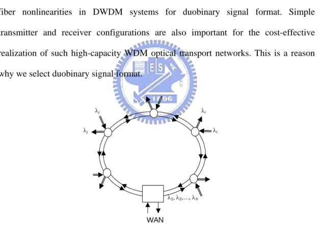
(13) z. Compact modulation spectrum.. z. Simple configuration of transmitter and receiver.. z. High fiber-nonlinearity tolerance.. In according to these requirement, optical duobinary format is very attractive, because their optical modulation bandwidth can be compressed to the data bit rate B, that is, the half-bandwidth of the nonreturn-tozero (NRZ) format (2B). A simple direct-detection receiver can be used in this format, which is also desirable for cost-effective realization for the receivers. It is strongly demanded to overcome the transmission distance limitation induced by both the dispersion characteristics and the fiber nonlinearities in DWDM systems for duobinary signal format. Simple transmitter and receiver configurations are also important for the cost-effective realization of such high-capacity WDM optical transport networks. This is a reason why we select duobinary signal format.. λj. λi. λj. λi. λ1, λ2,…, λN. WAN. Figure 1-1: Multi-Ring Passive Optical Network structure. 1.2 What is the Duobinary Modulation Format. 3.
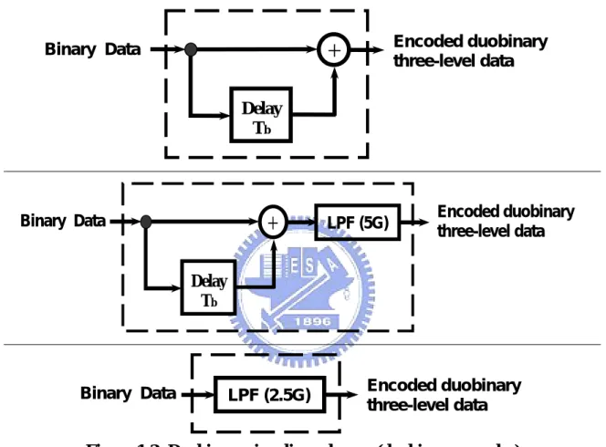
(14) Optical duobinary modulation (DBM) format is considered to be a technology of great importance for the next generation of optical transmission networks. The major factors is as following: z. Narrower spectrum bandwidth of optical signal (a half of the spectrum bandwidth of NZR).. z. High spectral efficiency for DWDM.. z. Excellent dispersion and nonlinear tolerance.. z. Using the intensity modulation direct detector (the same as the demodulation of NRZ).. z. Without dispersion management in Multi-ring passive optical network area.. Duobinary modulation is a scheme for transmitting scheme R bit/sec using less than R/2 Hz of bandwidth. Nyquist’s rule tells us that in order to transmit R bits/sec without intersymbol interference (ISI), the minimum bandwidth required of transmitted pulse is R/2 Hz. This result implies that the duobinary pulse will have ISI. However, this ISI is introduced in a controlled manner so that it can be subtracted out to recover the original values. With a narrower spectrum, the distortion effects of the channel are also fewer. This outcome is one of reasons why duobinary modulation is resilient to dispersion. One way of generating duobinary signal is to digitally filter data bits with two-tap finite impulse response (FIR) with equal weight and then low-pass filter the resulting signal to obtain the analog waveform with the function in Fig. 1-2. Duobinary signaling system also calls partial response signal system, because of the transmission signal with the dual information and its principle is shown in Fig 1-2. From Fig. 1-2, we can find duobinary encoder not only is used as encoder but also the finite impulse response (FIR) filter. Therefore, the spectrum of duobinary signal has 4.
(15) narrower bandwidth than NRZ signal about half of NRZ. Duobinary modulation with the signal modulation and coding technique is major advantage. As a result of these advantages, there are better transmission performances for the application of optical fiber transmission system.. Binary Data. Encoded duobinary three-level data. +. Delay Tb. Binary Data. +. LPF (5G). Encoded duobinary three-level data. Delay Tb. Binary Data. LPF (2.5G). Encoded duobinary three-level data. Figure 1-2: Duobinary signaling schemes (duobinary encoder). 1.3 Structure of The Thesis In Chapter 2, the theory and the math model of duobinary signal are described in detail, including the implement of optical duobinary transmission system. Chapter 3 I propose and experimentally demonstrate a new cost-effective way to implement PMDBM Transmission system using single Mach-Zehnder Modulator (MZM). The 5.
(16) effects of driving voltages and the bandwidth of duobinary filter are given in Chapter 4.and the simulation and experimental results can demonstrate the improvement by optimizing the driving voltages and the bandwidth of duobinary filter. Finally, conclusions are given in the chapter 5.. 6.
(17) CHAPTER 2 BASIC CONCEPTS OF DUOBINARY MODULATION FORMAT. 2.1 Duobinary signaling intersymbol interference (ISI) is an undesirable phenomenon that produces a degradation in system performance. Nevertheless, by adding ISI to the transmitted signal in a controlled manner, it is possible to achieve a signaling rate equal to the Nyquist rate of 2W symbols per second in a channel of bandwidth W Hertz. Such schemes are called correlative-level coding or partial-response signaling schemes. The basic idea of correlative-level coding will now illustrated by considering the specific transmission format of duobinary signaling, where “duo” implies doubling of transmission capacity of the straight binary system.. 2.1.1. The theory of duobinary coding. Consider a two-level amplitude input sequence b(k) consisting of uncorrelated amplitude 1 and 0, each having duration Tb. As before, this sequence is applied to pulse-amplitude modulator producing a two-level sequence of short pulse whose amplitude a(k) is defined by. {. ak =. +1 if symbol bk is 1 −1 if symbol bk is 0. (2-1). When this sequence is applied to a duobinary encoder, it is converted into a three-level output, namely –2, 0 and 2. To produce this transformation, we may use the scheme shown in Fig. 2-1. The two-level sequence a(k) is first passed through a simple filter involving a single delay element and summer. For every unit impulse applied to the input of this filter, we get two unit impulses spaced Tb seconds apart at the filter output. Therefore, we may express the duobinary coder output c(k) as the. 7.
(18) sum of the present input pulse a(k) and its previous value a(k-1), as shown by equation (2-2). c ( k ) = a ( k ) + a ( k − 1). (2-2). Filter H(f) a(K) Input two-level sequence. +. Hr(f) ∑. +. Band -limited filter. c(k) output sequence. Delay Tb. Figure 2-1 One of the effects of the transformation described by equation (2-2) is to change the input sequence a(k) of uncorrelated two-level pulses into a sequence c(k) of correlated three-level pulses. This correlation between the adjacent pulses may be viewed as introducing intersymbol interference into the transmitted signal in artificial manner. However, the ISI so introduced is under the designer’s control, which is the basis of correlative coding. Fig. 2-2 shows the variation between the duobinary encoder input and the output. Duobinary signal Two-level input sequence. Duobinary encoder. Figure 2-2: An ideal delay element, Tb second, has the frequency response exp ( jπ fTb ) , so that the frequency response of the simple delay-line filter in Fig. 2-1 is 1 + exp ( jπ fTb ) . First, we assume that the frequency response of the band-limited. filter Hr(f) is ideal magnitude response shown in Fig. 2-3.. 8.
(19) {. Hr (f ) =. 1 0. f ≤. 1 2Tb. (2-3). otherwise. Hr=(f). f 1/2Tb. 1/2Tb. Figure 2-3: Hence, the frequency response of duobinary encoder connected in cascaded with the band-limited filter is shown as. H ( f ) = H r ( f ) 1 + exp ( j 2π fTb ) . = H r ( f ) exp ( − jπ fTb ) + exp ( jπ fTb ) exp ( − jπ fTb ). (2-4). = 2 H r ( f ) cos (π fTb ) exp ( − jπ fTb ). Finally, the overall frequency response of the duobinary-signaling scheme has the form of a half-cycle cosine function, as shown by equation (2-5). {. Hr (f ) =. 2 cos (π fTb ) exp ( − jπ fTb ) 0. f ≤. 1 2Tb. (2-5). otherwise. The magnitude response and phase magnitude response for duobinary-signaling scheme are shown in Fig. 2-4 (a) and (b), respectively. An advantage of this 9.
(20) frequency response is that it can be easily approximated, in practice, by virtue of the factor that there is continuity at the band edge. The spectrum of duobinary signal is a half of the original signal, so duobinary signal has higher spectrum efficiency. arg |H|(f). π. |H|(f). 2. 2 Rb = 1/Tb. 0. Rb/2 f. -Rb/2. − -Rb/2. 0. Rb/2. f. π 2. Figure 2-4. From the first line in equation (2-4) and the definition of Hr(f) in equation (2-3), we find that the impulse response corresponding to the frequency response H(f) consist of two sinc pluses that are time-displaced Tb seconds with respective to each other, as shown by t t − Tb h ( t ) = sin c + sin c Tb Tb . =. =. =. sin (π t Tb ) sin π ( t − Tb ) Tb + π t Tb π ( t − Tb ) Tb sin (π t Tb ) sin (π t Tb ) − π t Tb π ( t − Tb ) Tb. (2-6). Tb 2 sin (π t Tb ). π t (Tb − t ). The impulse response h(t) is plotted in Fig 2-5, where we see that it has only two distinguishable values at the sampling instants. From the Fig. 2-5, we can see that the 10.
(21) tails of h(t) decay as 1/|t|2, which is a faster rate of decay than 1/|t| encountered in ideal sinc pulse so ISI can be reduced. That is why we also refer to this type of correlative coding partial-response signaling.. t sin c Tb . t − Tb sin c Tb . (a). h(t). Serious ISI is introduced when detecting the next symbol. No ISI is introduced when detecting the previous symbol. (b) Figure 2-5 11.
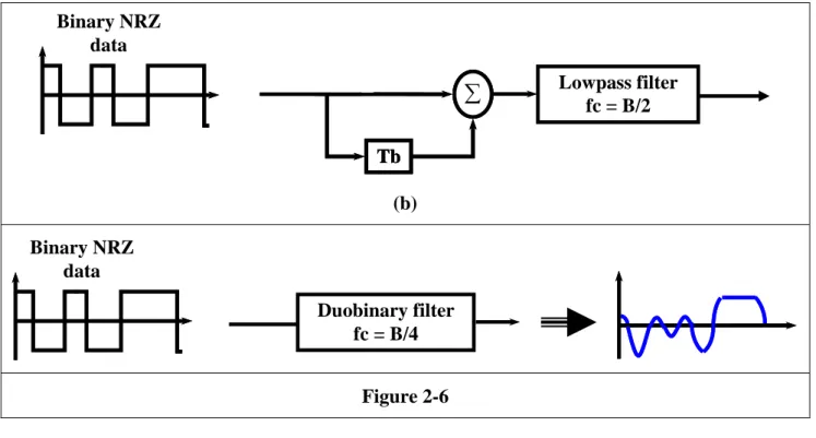
(22) 2.1.2. Implement of duobinary encoder. Two possible implementations of a duobinary generator are shown in Fig. 2-6. In Fig. 2-6(a), an ideal (no band limiting) binary NRZ signal is passed through a delay-and-add circuit, which has a periodic transmission response, to produce an ideal duobinary NRZ signal. The ideal duobinary signal may then be passed through a band-limiting filter resulting in finite rise and fall times between levels. Note that the band-limiting filter is not a requirement for the generation of a duobinary signal. However, it will be shown that this band-limiting filter is essential to obtain an improvement in the dispersion-limited transmission distance when using duobinary transmission. Alternatively, as shown in Fig. 2-6(b), a duobinary filter may be approximated by a single low-pass filter with a 3-dB cutoff at 0.25B the bit rate. Such a filter approximates the low-frequency roll-off of a delay-and-add circuit while concurrently filtering out frequency components above B/2. From the Fig. 2-6 we can see the difference between the duobinary encoder and duobinary filter are that the duobinary signal by using 5-th pole Bessel filter has less narrow signal spectrum, i.e. the high frequent components being reduced, and has the ripple in the null space.. Binary NRZ data. ∑ Tb. (a). 12.
(23) Binary NRZ data. ∑. Lowpass filter fc = B/2. Tb. (b) Binary NRZ data Duobinary filter fc = B/4. Figure 2-6. Figure 2-7: Simulation of different dupbinary encoder.. 2.1.3. Generate the optical dobinary signal. 13.
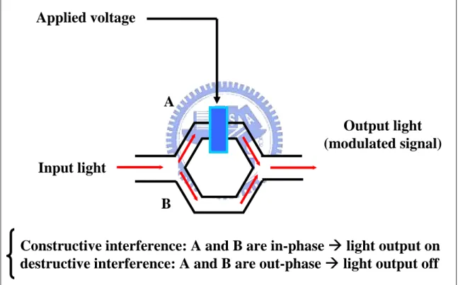
(24) In this section, I focus on how to convert the three-level electrical duobinary. 1. signal into optical duobinary signal with 0 two intensity levels. At first, we will discuss the Mach-Zehnder modulator how to modulate signal. Fig. 2-7 shows the structure of MZ modulator. When applied voltage is added on the electrode of the MZ modulator, it induces an electric field, which will change the index of refraction and changes the relative phase of the signal in the arm. Signal A and B will interfere each other when they combine at the modulator output. By this property, we can make the constructive or destructive interference to modulate signal.. Applied voltage. A Output light (modulated signal) Input light B Constructive interference: A and B are in-phase Æ light output on destructive interference: A and B are out-phase Æ light output off Figure 2-8: The structure of MZM. In general, the optical duobinary signal can be generated, by using a dual-arm Mach–Zehnder (MZ) type with push–pull operation and then I will describe operation method for dual-arm MZ modulator to generate the optical duobinary signal. Fig. 2-8(a) shows that MZ modulator is driven by duobinary signal and its inverted signal using the push-pull type and Fig. 2-8(b) shows operation method and transfer curve of MZ modulator. The output electric field E(t) is expressed as. 14.
(25) {. E = E0 a ⋅ b ⋅ e j∆φ1 + 1 − a 2 1 − b 2 e j∆φ2. } (2-12). 1 for perfect splitting ratio : a = b = 2 1 1 E = E0 e j∆φ1 + e j∆φ2 2 2 ∆φ − ∆ φ 2 j = E0 ⋅ cos 1 ⋅e 2 2 ∆φ − ∆φ2 power = E0 cos 2 1 2 . (2-13) ∆φ1 +∆φ2 2. (2-14) (2-15). where E 0 is the input electric field and φ (t) is the phase difference between the. propagation in the two optical waveguides and φ0 is the constant when the MZ modulator is driven with push-pull operation. E-field and Power of LiNbO3 Modulator 1 0.8. Transmission function. 0.6 0.4 0.2 0 -0.2 -0.4 -0.6 -0.8 -1 0. e-field power 1. 2. 3 4 phase difference. 5. 6. Figure 2-9: The transmission curve of MZM. 15.
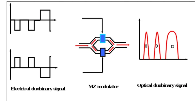
(26) Optical phase of output signal π π. 0. Data Transmittance. U. 0 C. A. B. L Data. Dual-drive Mach-Zehnder modulator. -1. 0. 1. Electrical duobinary signal. Figure 2-10: The transmission curve of MZM. At first, the modulator has to be biased at its null point B. Therefore, adjusting the amplitude of the modulator driving signal so that logic states "-1","0", and "1" of the duobinary encoded signal are set at points "A", "B", and "C" in Fig. 2-8 (b), generates the optical duobinary signal. The symbols "-1" and "1" of the duobinary encoded signal are represented by "on" state of optical signal with the phase 0 and π, respectively. Although the generated optical duobinary signal has three-level intensity in terms of electric field, it only has two-level intensity in terms of optical power, as shown in Fig 2-9.. 16.
(27) 0. Electrical duobinary signal. MZ modulator. 0. π. Optical duobinary signal. Figure 2-11: The schemata of interference between TE and TM mode. 2.2 Duobinary decoding 2.2.1. Duobinary decode scheme. Original two-level sequence a(k) may be detected from the duobinary-coded sequence c(k) by invoking the use of equation, c(k) = a(k) + a(k-1). Specifically, let a(k) represent the estimation of the original pulse a(k) as conceived by receiver at. time t = kTb. Then, subtracting the previous estimate "a(k-1)" form c(k), we get ) a ( k ) = c ( k ) − a ( k − 1). (2-16). It is apparent that if c(k) is received without error and if also the previous estimate a(k-1) at time t = (k-1)Tb corresponds to a correct decision, then the current estimate a(k) will be correct too. The technique of using a stored of the previous symbol is call. decision feedback. We observe that detection procedure just described is essentially an inverse of the operation of the simples delay-line filter at transmitter. Duobinary decode scheme is shown in Fig 2-10.. 17.
(28) C(K) Receive sequence. +. ∑ -. c(k) - a(k-1) > 0, a(k) = 1 c(k) - a(k-1) < 0, a(k) = -1. a(k). a(k-1) Delay Tb. Figure 2-12. 2.2.2. Error propagation. A major drawback of this detection procedure for duobinary encode is that once errors are made, they tend to propagate error to the next information because a decision on the current input b(k) depend on the correctness of the decision made on the previous input b(k-1). Error propagation is caused because of the relation of the adjacent data. Form Fig. 2-11, we can find the decoding rule for duobinary encode and the source of the error propagation.. 18.
(29) a(k). C(k). ∑. + +. a(k-1). If c(k) = -2 Æ a(k) = -1. Delay Tb. If c(k) = 0 Æ a(k) = -a(k-1) Error propagation term a(k). a(k-1). c(k). -1. -1. -2. 1. -1. 0. -1. 1. 0. 1. 1. 2. If c(k) = -2 Æ a(k) = 1. Figure 2-13. Finally, I give an example shown in table 1. In this example, the receiver may receive the error signal r(k) because of additional noise and then we can find the error propagate to the next information. Binary sequence b(k). 0. 0. 1. 0. 1. 1. 0. 1. Two-level sequence a(k). -1. -1. 1. -1. 1. 1. -1. 1. Delay of sequence a(k), a(k-1). -1. -1. -1. 1. -1. 1. 1. -1. Duobinary coder output c(k). -2. -2. 2. 0. 0. 2. 0. 0. Receive signal r(k). -2. -2. 2. 2. 0. 2. 0. 0. 0. 0. 1. 1. 0. 1. 0. 1. Applying decision rule. Error propagation. Table2-1. 19.
(30) 2.1.3. Differential encoder A practical means of avoiding the error-propagation phenomenon is to use. precoding before the duobinary coding, as shown in Fig. 2-12. The precoding operation performed on the binary data sequence b(k) converts it into another binary sequence d(k) defined by d ( k ) = b ( k ) ⊕ d ( k − 1). (2-17). where symbol ⊕ denotes modulo-two addition of the binary digits b(k) and d(k-1). This addition is equivalent to a two input Exclusive OR operation, which is performed as follows: b(k). d(k). d(k-1) T. Differential encoder b(k). d(k-1). d(k). 0 0. 0 1. 0 1. 1. 0. 1. 1. 1. 0. Figure 2-14. The precoded duobinary scheme is shown in Fig. 2-13. The precoded binary sequence d(k) is applied to a pulse-amplitude modulator, producing a corresponding two-level sequence of short pulse is next to applied to duobinary coder, thereby producing the sequence c(k) that is related to a(k) as follows: 20.
(31) c ( k ) = a ( k ) + a ( k − 1). (2-18). Note that unlike the linear operation of duobinary coding, the precoding described by formula (2-9) is a nonlinear operation. The combined use of the equations (2-9) and (2-10) yields. {. c (k ) =. If If. 0 ±2. c (k ) < 1 c (k ) > 1. if data symbol b ( k ) is 1 if data symbol b ( k ) is 0 ⇒. symbol b ( k ) is 1 symbol b ( k ) is 0. b(k). a(k). Pulse amplitude modulator. d(k). d(k-1). (2-19). ∑. +. C(k). +. T. Delay Tb. a(k-1). Differential encoder. b(k). d(k-1). d(k). a(k). a(k-1). c(k). 0. 0. 0. -1. -1. -2. 0. 1. 1. 1. 1. 2. 1. 0. 1. -1. 1. 0. 1. 1. 0. 1. -1. 0. Figure 2-15. When | c(k) | = 1, the receiver simply makes a random guess in favor of symbol 1 or 0. According to decision rule, the detector consists of a rectifier, the output of which is compared in a decision device to a threshold of 1. A block diagram of the detector is is show in Fig. 2-14. A useful feature of this detector is that no knowledge of any. 21.
(32) input sample than the present one is required. Hence, error propagation cannot occur in the detector of Fig. 2-14. | c(k) | c(k) Rectifier. symbol b ( k ) is 1 symbol b ( k ) is 0. Decision device. If. c (k ) < 1. If. c (k ) > 1. Threshold = 1. Figure 2-16. By using the differential encoder, receiver circuit can be reduced and system performance is upgraded because of no error propagation. So the differential encoder has become indispensable to duobinary transmission system, especially optical duobinary transmission.. 2.3 Optical duobinary transmission system There are several approaches to achieve overall bandwidth efficiency. Amongst them are improved modulation formats, channel coding, and sophisticated management of chromatic and polarization mode dispersion including equalization, wideband optical amplifiers, improved WDM-multiplexers and demultiplexers. Sophisticated modeling of the WDM-optical channel including nonlinear effects is necessary in order to investigate the impact of the various methods. For practical reasons it is important to end up with structures that are realizable at these high frequencies i.e. we have to avoid high complexity algorithms. In this contribution we focus mainly on bandwidth efficient modulation formats at channel data rates of 10 Gb/s. By saving bandwidth both the dispersion problems and the channel density are improved.. 2.3.1. Optical duobinary transmitter. 22.
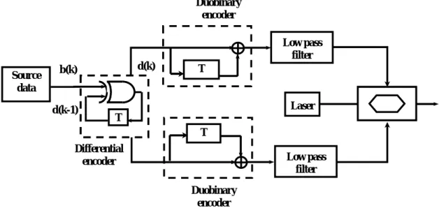
(33) The Fig. 2-15 shows transmitter for optical duobinary system using dual arm MZ modulator with push pull operation.. Duobinary encoder Low pass filter Source data. d(k). b(k). d(k-1). T. Laser T T. Differential encoder. Low pass filter Duobinary encoder. Figure 2-17: The schemata of interference between TE and TM mode. A partial response encoded sequence c(k) is related to binary sequence d(k) by the following encoding rule c ( k ) = d ( k ) + d ( k − 1). (2-20). The output symbols are 0, 1,and 2. Using an offset of -1 the output symbols change to –1, 0 and 1 without changing the encoding scheme itself. Decoding the received bits without recursion is possible by using a differential encoder as precoder in front of the duobinary encoder. The precoding rule for duobinary coding is d ( k ) = b ( k ) ⊕ d ( k − 1). (2-21). where " ⊕ " is the logic instruction " exclusive or ". The detail signal procedure is shown in Fig. 2-16 (a) and (b). Therefore the intensity profile of duobinary signal is the same as the binary intensity modulated when AM-PSK.. 23.
(34) c(k). d(k). b(k) d(k-1). Offset -1. a(k) V1. Vb1 Output. T. T Differential encoder. V2. b(k). d(k-1). d(k). c(k). 0. 0. 0. 0. -1. 1(on). 0. 1. 1. 2. 1. 1(on). 1. 0. 1. 1. 0. 0(off). 1. 1. 0. 1. 0. 0(off). output. Duobinary encoder. a(k) Output. (a). Vb2. 0 Respective phase. a(k) = -1 a(k) = 0. π. a(k) = 1. (b) (c) Figure 2-18: (a) the diagram for optical duobinary encoding. (b) the table for encoder procedure. (c) operation of MZ modulator. The principle of operation of the proposed scheme is shown in Fig. 1. The precoded. (2-22) duobinary are fed into the dual-drive Mach-Zehnder (DD-MZM). The output electric field Eout can be written as:. where Vπ is the switching voltage of the modulator and Vb1 and Vb2 are the DC bias voltages for arm one and arm two, respectively. V1 and V2 are the total voltages employed on the two electrode arms. The optical duobinary signal has two intensity levels " on " and " off " as shown in Fig. 2-16 (c). The " on " state signal can have one of two optical phases, 0 and π. As shown in Fig. 2-16 (b) and (c), the two " on ". 24.
(35) states correspond to the logic states "1" and "-1" of the duobinary encoded signal, a(k), and the "off " state corresponds to the logic state “0” of the duobinary encoded signal. According to the duobinary encoding rule, the logic states "1", "0" and "-1" of the duobinary encoded signal correspond to the logic states "1", "0" and "0" of the original binary signal, respectively. Therefore, the original signal can be recovered by inverting the directly detected signal. As the photodiode converts the optical duobinary signal to the electrical binary signal, no duobinary decoder is needed. The detected signal must be inverted to recover the original binary signal, so logic inverter is needed for data recovery. Fig. 2-17(a) shows the simple model of the proposed optical duobinary transmission system. The original binary signal, duobinary encoded signal, optical duobinary signal and receiver output signal are also shown in Fig. 2.17(b). (B). (A) Source data. Precoder. (C) Duobinary encoder. O/E converter. Output. E/O converter. Inverter. Decision. (D). (E) Original binary signal. (A). 0. 1. 0. 1. 1. 0. 0. 1. 0. 0. 1. 0. 0. 1. c(k) = c(k-1) ⊕ a(k) Differential encoded signal (B). 0. 1. 1. 0. 1. 1. 1. 0. c(k) = a(k-1) + a(k). Duobinary encoded signal. (C). E/O converter. Optical duobinary signal. (D). 25. Square law decision and data inverted.
(36) 2.3.2. Analysis of the signal spectrum. The modulated optical signal s(t) can be expressed as. (2-23) where A and wc are amplitude and angular frequency of optical carrier, respectively. S(t) is the optical duobinary signal if d(t) is the duobinary encoded signal which has three values of 1, 0, and -1. S(t) is the binary IM signal if is the binary signal which has two values of 0 and 1. The power spectrum of the duobinary-encoded signal is expressed as. (2-24) where T denotes one bit duration. Fig. 2-18 shows the power spectra of the duobinary encoded signal and binary signal in the baseband.. Fig. 2-19: 10 Gb/s power spectra density for NRZ signal (upper trace) and duobinary signal (lower trace). The optical duobinary signal power is concentrated within a narrow bandwidth, half the binary NRZ signal spectrum, as shown in Fig 2-18. Such a narrow band signal can be expected to achieve high tolerance to chromatic dispersion. From the Fig 2-19, we 26.
(37) can find that the optical duobinary signal has no carrier frequency component in contrast with the binary IM signal. Therefore, fiber input power limitation due to SBS can be expected to be relaxed. This means the optical duobinary signal has more nonlinearity tolerance than NRZ signal.. (a). (b) Fig 2-20: (a) Power spectrum of optical duobinary signal (b) Power spectrum of NRZ signal. Finally, the main advantages for using optical modulation format in high-speed modulation systems can be summarized as followed as: 1. High dispersion tolerance 2. High nonlinearity tolerance 3. High spectrum efficiency 4. Intensity modulation direct detection 27.
(38) CHAPTER 3 THE PAHSE-MODULATION DUOBINARY MODUALTION FORMAT In this chapter, I proposed and experimentally demonstrated a cost-effective chirped duobinary modulation scheme to improve the self-phase modulation (SPM) tolerance using only one modulator. Penalty-free transmission is achieved after 230kmof standard single mode fiber. Compared with no phase modulation, I observed a 12dB sensitivity improvement.. 3.1 Introduction of Phase-Modulation DuoBinary modulation format Recently, optical duobinary modulation (DBM) has receiverd much attention .Because of narrow spectral bandwidth, DBM has higher specral efficiency, better chromatic dispersion tolerance and less sensitivity to nonlinear effects. There benefits are essential advantages for dense wavelength division multiplexed (DWDM) transmission systems. However, under high input power, the spectral width broadens rapidly during transmission due to the Self-Phase Modulation (SPM) effect. Therefore, dispersion tolerance was weakened quickly when increased the input power. Pre-chirped duobinary modulation was first proposed in 1998, and the theoretical investigation was given to explain the benefits of phase modulation. The phase-modulation duobinary modulation (PMDBM) was later suggested to improve SPM tolerance by combining the effects of phase modulation, chromatic dispersion and SPM. In order to provide the required phase modulation, an extra modulator is needed. Therefore, this will increase the complexity and cost of the transmitter, and hamper the use of this modulation format in cost-sensitive metro area transmission systems. In this chapter, I proposed a novel chirped duobinary transmission scheme to improve the SPM tolerance using only one modulator. After 230km transmission of 28.
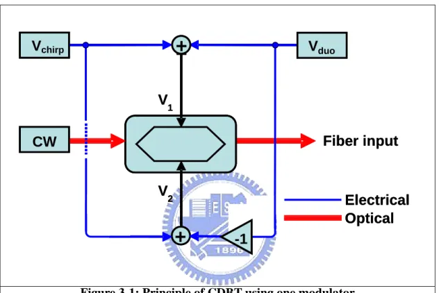
(39) standard single mode fiber (Corning SMF-28), we observed a 12dB sensitivity improvement.. 3.2 The operation principle of PMDBM 3.2.1. Using only one MZM for modulating phase and intensity. The principle of operation of the proposed scheme is shown in Fig3-1. The precoded duobinary electric signal and phase data are combined and fed into the Dual-Drive Mach-Zehnder Modulation (DD-MZM). I assumed that the DD-MZM is a ideal Electric-Optical Modulator (E/O Modulator), i.e. the Extinction Ratio (ER) of DD-MZM is infinity. The operation equation of DD-MZM (3-1) is shown. The output electric field Eout can be written as:. Eout =. Ein j (e 2. θ1. Ein j = e 2 . +ej. θ2. θ1 − θ 2 2. . ). +e. (3-1) θ + θ2 − j 1 2 . j ⋅e . θ1 + θ 2 2. . θ1 + θ 2 2 . θ − θ 2 j = Ein Cos 1 ⋅e 2 Q θ1 =. V1 π Vπ. θ2 =. V2 π Vπ V1 +V2 π 2Vπ . V − V j = Ein Cos 1 2 π ⋅ e 2Vπ V1 = Vduo + Vchirp + Vbias1 V2 = −Vduo + Vchirp + Vbias 2. Eout. 2Vchirp +Vbias 1 +Vbias 2 π 2Vπ . 2V + V − V j = EinCos duo bias1 bias 2 π ⋅ e 2Vπ . where V π is the switching voltage of the modulator and Vbias1 and Vbias2 are the DC. 29.
(40) bias voltages for arm one and arm two, respectively. V1 and V2 are the total voltages employed on the two electrode arms. Using the property of DD-MZM, we can modulate the optical signal phase and intensity with only one MZM for high cost-efficiency.. + +. Vchirp PM. Vduo duo. V1 Fiber input. CW V2. Electrical Optical. +. -1. Figure 3-1: Principle of CDBT using one modulator. 3.2.2. The operation principle of chirp inducing by phase modulation. By carefully choosing the polarity sent into the two arms, we can control the duobinary data (Vduo) appears only on the intensity term and the phase modulation data (Vchirp) appears only on the phase term. Therefore, by using a single modulator, we can simultaneously encode the duobinary and phase information onto the optical signal. Fig3-2 shows (a) the detail pattern of normalized electrical duobinary data, (b) the detail pattern of normalized electrical phase data ( data ), (c) normalized optical intensity of PMDBM, (d) normalized optical phase of PMDBM, (e) normalized 30.
(41) optical intensity data of PMDBM with color-encoded frequency chirped, respectively. Although we shows inverted signals in (a) and (b), we do have the freedom to select using either data or data in phase modulation signal. In addition, (c) and (d) are the corresponding optical intensity and phase after PMDBM. In Fig 3-1 (e), we shown the frequency shift due to phase modulation by color encoded bit pattern. There is a blue-shifted at the rising edge and red-shifted at the falling edge. We can see that the rising and falling edges have different frequency chirped.. Intensity. Duobinary Data. 0.5 0. 0.5. 1 1.5 2 2.5 Phase Modulation Data. 3. 1. (b). 0.5 0. 0. 0.5. 1 1.5 2 Intensity of PMDBM. 2.5. 1 0. 3. (c). 0.5. phase. Intensity. Intensity. 0. Intensity. (a). 1. 0. 0.5. 1. 1.5 2 Phase of PMDBM. 2.5. 3. 1 0 -1 0. (d) 0.5. 1. 1.5. 2. 2.5. 1. 3. (e). 0.5 0. 0. 0.5. 1. 1.5 2 time (ns). 31. 2.5. 3.
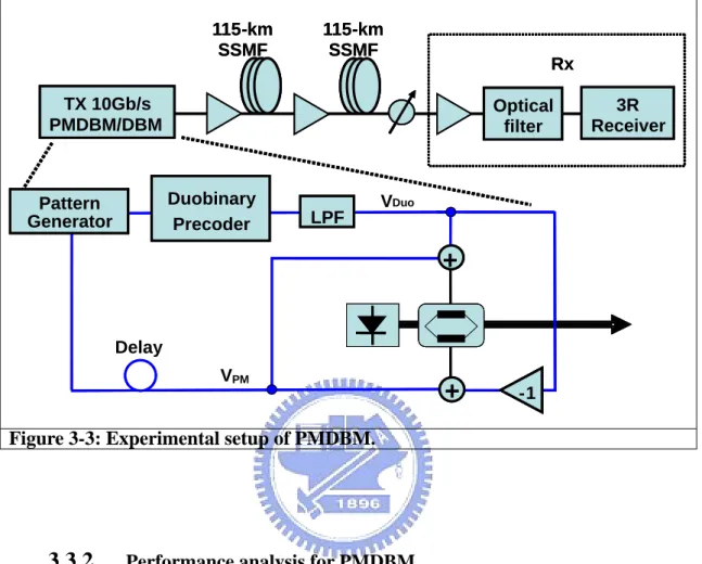
(42) Figure 3-2: (a) Electrical bit pattern of duobinary data (b) Electrical bit pattern of phase data (c)Optical intensity pattern after modulator (d)Optical phase pattern after modulator (e)the chirped duobinary signal. By choosing the appropriated amplitude and sign of the electrical phase bit pattern, we can control the needed amount of phase modulation to counterbalance the effects of SPM and chromatic dispersion under different optical powers and transmission distance.. 3.3 Experimental setup and performance analysis of PMDBM 3.3.1. Experimental setup of PMDBM. Fig.3-3 shows the experimental setup of PMDBM. A 10Gbps pseudo-random binary sequence (PRBS) of length of 215-1 is sent into Inphi 13750DE duobinary pre-coder. The electrical signal then passes through duobinary encoder (a 2.5GHz, 5th order electrical Bessel low pass filter (LPF)) to generate the duobinary signal. Then the electrical duobinary and phase data are combined using a wideband (40GHz) resistive combiner and sent into the Dual-Drive MZM with V π. equals to 5.8 volt. Due to. the high insertion loss of combiner (7.5dB), the maximum driving voltage we can obtain after the combiner is 3.8 volt for both the duobinary data and phase modulation data, which corresponding to about 66% of the full swing voltage. The CW laser is a JDSU/CQF935 40mw DFB laser with center wavelength at 1549nm and the input optical optical power sent into the fiber is set at 13dBm to ensure a large SPM effect. After 115km of SSMF, an EDFA is used to amplify the optical power back to 13dBm before sent into another section of 115km of SSMF.. At the receiver, I employed an. optically pre-amplified receiver including an EDFA and a 40GHz optical band-pass filter. 32.
(43) 115-km SSMF. 115-km SSMF. Rx. TX TX 10Gb/s 10Gb/s PMDBM/DBM PMDBM/DBM. Optical Optical filter filter. Duobinary Duobinary Precoder Precoder Encoder. Pattern Pattern Generator Generator. LPF. 3R 3R Receiver Receiver. VDuo. +. Delay VPM. +. -1 -1. Figure 3-3: Experimental setup of PMDBM.. 3.3.2. Performance analysis for PMDBM. At back-to-back measurement, the receiver sensitivity (bit error ratio (BER)=10-9) is -32dBm. The eye pattern of 66% driving voltage of (a) 0km DBM, (b) 230km DBM, (c) 0km CDBT, (d) 230km CDBT are shown in Fig.3-4 We can see the chirp inducing by phase modulation has significant impact on the eye pattern by maintaining the balance between SPM and dispersion. DBM 0km. 33.
(44) PMDBM 0km. DBM 230km. PMDBM 230km. 34.
(45) Figure 3-4: The simulation (red) and experimental (blue) eye pattern of PMDBM and DBM in 0km & 230km. Fig.3-5 (a) and (b) show the spectral of 66% DBM and PMDBM before and after transmission. We observe a wider spectrum of PMDBM before transmission. Nonetheless, we notice a narrower spectrum after the transmission. This is the another evidence shown the effect of phase modulation can maintain a narrower spectrum after transmission and has better dispersion tolerance Fig3-6. shows the BER of 0km and 230km transmission of 66% driving voltage DBM as reference. Compared with 66% PMDBM, we can not obtain error free transmission after 230km for both 66% and 100% DBM. This corroborates well with the walk-off eye pattern in Fig3-4. and the optical spectra shown in Fig3-5. Conversely, if we applied appropriate amount of phase modulation, we achieved penalty-free transmission after 230km transmission of SSMF. .. 35.
(46) Spectrum of DBM and PMDBM at 0km -10 DBM 0 km PMDBM 0 km. Power (dBm). -20 -30 -40 -50 -60 -70 1549.1. 1549.2. 1549.3 1549.4 wavelength (nm). 1549.5. 1549.6. Spectrum of DBM and PMDBM at 230 km -10 DBM 230 km PMDBM 230 km. Power (dBm). -20 -30 -40 -50 -60 -70 1549.1. 1549.2. 1549.3 1549.4 wavelength (nm). 1549.5. 1549.6. Figure 3-5: Optical spectra of 66% driving voltage of (a) 0km DBM, (b) 230km DBM, (c) 0km PMDBM, (d) 230km PMDBM. 36.
(47) 10. 10. 10. 10. 10 10 10 10 10 10. BER of DBM and PMDBM. -2. PMDBM 66% 0 km PMDBM 66% 230 km DBM 66% 0 km DBM 66% 230 km NRZ 100% 0 km DBM 100% 0 km. -3. -4. -5. -6. -7 -8 -9. -10 -11. -40. -35. -30 Received Power (dBm). -25. -20. Figure 3-6: BER of 66% driving voltage of 0km and 230km of DBM and PMDBM, NRZ format and 100% driving voltage of DBM. 3.3.3. Performance comparison with DBM in linear & nonlinear. Because the high insertion loss of combiner (7.5dB), we can not transmission in 100% driving voltage of PMDBM. The future work is to do the fully driving PMDBM using the low driving voltages MZM. Therefore, there is signal distortion form using only 66% driving voltage. First, I compare the PMDBM in linear and nonlinear. The experimental results can demonstrate that the effect of phase. 37.
(48) modulation counterbalances the signal distortion from SPM and dispersion. Because the effect of SPM only appears in nonlinear region. From the experimental result, we can see that there is the more improvement for PMDBM in nonlinear region than in linear region. The chirp induced by phase modulation can compensate the over nonlinear effect, like SPM when the appropriate amount of SPM can increase the dispersion tolerance. PMDBM can increase the tolerance of dispersion and nonlinear effect by applying appropriate amount of phase shift.. Figure 3-7: The sensitivity of PMDBM (66%) in linear & nonlinear.. Due to the high insertion loss of combiner, we can not transmit the PDBDM signal in fully drive. The effects of lower driving voltage distort the duobinary signal. Fig3-7. shows that the worse sensitivity curve in lower driving voltages as Chapter 3 mentioned. Therefore, we can see that the improvement of PMDBM makes the sensitivity curve better than 50% driving voltage DBM in linear. Basically I can infer 38.
(49) that the improvement of phase modulation is decreased by the effect of lower driving voltage because the most appropriate duobinary filter is not 2.5GHz bandwidth in 66% driving voltage. .. -25 PMDBM 66% Nonlinear DBT 100% Linear DBT 75% Linear DBT 50% Linear. Sensitivity(dBm). -30. -35. -40. 0. 50. 100. 150 Distance(km). 200. 250. Figure 3-8: The sensitivities of PMDBM (66% in nonlinear region) and DBM (in linear region) in different driving voltage.. 3.4 Summary of the experimental eye diagram and BER curve 3.4.1. The eye diagrams of PMDBM in nonlinear. 0 km. 39.
(50) 50 km. 75km. 100 km. 40.
(51) 125km. 150km. 180km. 41.
(52) 205km. 230km. 255km. 42.
(53) Figure 3-9: The electric (left) and optical (right) eye diagrams of nonlinear PMDBM (66% driving voltage) in different transmission distance.. 3.4.2. The eye diagrams of PMDBM in linear. 0 km. 50 km. 75km 43.
(54) 100 km. 125km. 150km. 44.
(55) 180km. 205km. 230km. 45.
(56) Figure 3-10: The electric (left) and optical (right) eye diagrams of linear PMDBM (66% driving voltage) in different transmission distance.. 46.
(57) CHAPTER 4 THE EFFECT OF DRIVING VOLATGES AND DUOBINARY FILTER. 4.1 Introduction In a duobinary transmission system, we use the low pass filter to generate duobinary three-level filter. In experiment process, we have to use a amplifier driver to amplify the electric signal for the driving voltage of MZM. Therefore, we can adjust the bandwidth of duobinary encoders by controlling the driving voltage and the bandwidth of duobinary filter. .. 4.2 The effect of driving voltage 4.2.1. Operation principle of driving voltage SSMF SSMF. SSMF. SSMF. Rx. TXTX10Gb/s 10Gb/s. 3R Receiver. PMDBM/DBM. DBM. 10 Gb/s. Pulse pattern generator. Q. Duobinary filter. Modulator driver. Differential encoder. Q. Duobinary filter. Modulator driver. Figure 4-1: The experimental setup In fig. 4-2, we can see the transmission function of MZM. By adjusting the gain controlling voltage of amplifier driver we can change driving voltage. In experiment and simulation system, we try the 100% 50% 25% driving voltage into MZM.. 47.
(58) Figure 4-2: The transmission curve of MZM. 4.2.2. Experimental and simulation results of driving voltage effect. Figure 4-3: The spectrum of different driving voltage 48.
(59) In fig 4-3, we can see the effect on signal spectrum by adjusting the driving voltage. In lower driving voltage, the spectrum of duobinary signal is narrower. Therefore, We can control the driving voltage to adjust the bandwidth of signal. We use the 2.5GHz 5th Bessel LPF in different driving voltage in linear and nonlinear region. From the sensitivity curve, we can see that the performance is getting worst in lower driving voltage when we use 2.5GHz LPF. We can get the same result in nonlinear region. In next section we will have a discussion about the bandwidth of duobinary filter.. Sensitivity(dBm) vs Distance(km) -24. 100% 2.5G linear 50% 2.5G linear 25% 2.5G linear. -26. S ensitivity(dBm ). -28. -30. -32. -34. -36. -38. 0. 25. 50. 75. 100 125 150 Distance(km). 175. 200. 225. 250260. Figure 4-4: The experimental results of different driving voltage in linear region. 49.
(60) Sensitivity(dBm) vs Distance(km). -26 100% 2.5G Nonlinear 50% 2.5G Nonlinear 25% 2.5G Nonlinear. -28. S ensitivity(dBm ). -30. -32. -34. -36. -38. -40. 0. 20. 40. 60. 80. 100 120 Distance(km). 140. 160. 180. 200. Figure 4-5: The experimental results of different driving voltage in nonlinear In fig 4-6, we can see the experimental and simulation eyes in different driving voltages. From the experimental and simulation eyes, we can explain the performance. First we can see the noise of mark is getting worse and the ripple of eyes is reduced. The two factor can dominate the sensitivity performance. The ripples of eyes cause the penalty from the extinction ratio decreasing. And the noise of mark is getting worse, too.. 50.
(61) 0km 100%. 0km 50%. 0km 25%. Figure 4-6: experimental and simulation eye in different driving voltage in 0km. 4.3 The effect of duobinary filter 4.3.1. Introduction of duobinary filter. In this section we have a detail discussion about the bandwidth of duobinary filter. In duobinary transmitter, duobinary filter is the duobinary encoder instead of delay&add circuit and band-limited filter (a half of bit rate). By adjusting the bandwidth of duobinary filter, we can find the best bandwidth of duobinary signal theoretical. Because we have no other different bandwidth filter, we have simulation results only.. 51.
(62) 4.3.2. The simulation results of duobinary filter. The simulation software for optical fiber transmission we used is VPItransmissionMaker. In fig 4-7 we can see the effects on the duobinary signal when we use different bandwidth duobinary filter.. Original data. Encoded data. 52.
(63) 3-level signal (3GHz duobinary filter). 3-level signal (2.5GHz duobinary filter). Optical signal (3GHz duobinary filter). Optical signal (2.5GHz duobinary filter). Optical eye (3GHz duobinary filter). Optical eye (2.5GHz duobinary filter). Figure 4-7: simulation pattern and eyes for 3GHz and 2.5GHz duobinary filter. 53.
(64) From the simulation eyes we can find the effect of duobinary filter on signal eye is like the effects of driving voltage. In the same way, the effects of duobinary filter dominate the noise of mark and ripples. In fig4-8. we can find the optimum bandwidth of duobinary filter. That is to say, there is a best bandwidth in specific driving voltage and transmission distance.. 100% driving voltage in 2GHz,2.5GHz,3GHz Sensitivity(dBm) vs Distance(km) -24 100% 2.0 100% 2.5 100% 3.0. -26. Sensitivity(dBm). -28. -30. -32. -34. -36. -38 0. 25. 50. 75. 100 125 150 Distance(km). 175. 200. 50% driving voltage in 2GHz,2.5GHz,3GHz. 54. 225. 250260.
(65) Sensitivity(dBm) vs Distance(km) -28. 50% 2GHz 50% 2.5GHz 50% 3GHz. -29 -30. Sensitivity(dBm). -31 -32 -33 -34 -35 -36 -37 -38 -39. 0. 25. 50. 75. 100 125 150 Distance(km). 175. 200. 225 240. 25% driving voltage in 2GHz,2.5GHz,3GHz Sensitivity(dBm) vs Distance(km) -20 25% 2GHz 25% 2.5GHz 25% 3GHz. -22 -24. Sensitivity(dBm). -26 -28 -30 -32 -34 -36 -38 0. 20. 40. 60. 80. 100 120 Distance(km). 140. 160. 180. 200. Figure 4-8: Simulation sensitivity curve in different driving voltage and filter. 55.
(66) In fig4-8, we can see that the best performance in the lower driving voltage have to use the wider bandwidth duobinary filter. Actually, we can get a optimum signal bandwidth for duobinary transmission system in specific transmission distance.. 4.4 performance analysis of driving voltage and duobinary filter 4.4.1. summary simulation eyes. From the fig 4-9, we can see the change of eyes clearly. We have to notice the ripples and the noise of mark. The two factors dominate the performance in back to back. 25% 3GHz. 25% 2.5GHz. 25% 2GHz. 50% 3GHz. 50% 2.5GHz. 50% 2GHz. 100% 3GHz. 100% 2.5GHz. 100% 2GHz. Figure 4-9: simulation eyes in 0km. 56.
(67) After transmitting 205km, we have to pay an attention to dispersion penalty. Therefore, we need to control a wider bandwidth of signal spectrum for reducing the noise of mark. But the wider bandwidth of signal spectrum cause more dispersion penalty. In fig4-10, we can see the dispersion penalty clearly . 25% 3GHz. 25% 2.5GHz. 25% 2GHz. 50% 3GHz. 50% 2.5GHz. 50% 2GHz. 100% 3GHz. 100% 2.5GHz. 100% 2GHz. Figure 4-10: simulation eyes after 205km. 4.4.2. Optimize the duobinary filter in specific condition. From the simulation eyes and the sensitivity curves, we know that the relation of the noise of mark and dispersion penalty is trade-off. We just can find the optimum setup.. 57.
(68) Filter DV. The noise of mark. Trade-off. DV. Dispersion penalty. Filter Ripple ( b2b) Figure 4-11: The relation of the noise of mark and dispersion penalty In table4-1, we can see that the lower driving voltage have to use a wider duobinary filter. There is a suitable bandwidth of signal spectrum combined by the effect of driving voltage and duobinary filter.. 100% DV 75% DV 50% DV 25%DV. 0km 2.3GHz 2.3GHz 2.9GHz 2.9GHz. 100km 2.3GHz 2.5GHz 2.5GHz 3.5GHz. 225km 2.5GHz 2.9GHz 3.1GHz 3.5GHz. Table 4-1: optimum duobinary filter in specific driving voltage and distance.. 58.
(69) CHAPTER 5 CONCLUSION 5.1 Phase-modulation duobinary transmission system We have successfully demonstrated a novel PMEDBM scheme to counter balance the effects of SPM and dispersion using only a single modulator. In PMDBM transmission system we can transmit 230km without penalty and longest transmission distance over 255km. In table 5-1, we can see the penalty in different transmission distance.. Fiber length (km) 50km 75km 100km 125km 150km. Penalty Fiber length Penalty (dB) (km) (dB) -3.5dB 180km -4.4dB (-35.5dBm) (-36.4dBm) -4.6dB 205km -1.17dB (-37.6dBm) (-33.17dBm) -6.48dB 230km 0dB (-38.48dBm) (-32dBm) -6.32dB 255km 6.3dB (-38.32dBm) (-25.7dBm) -6.12dB (-38.12dBm). Table 5-1 penalties of PMDBM transmission system. 5.2 The impact of driving voltages and duobinary filter Driving voltages and duobinary filter is a major factor in the performance of duobinary transmission system. In my simulation and experimental results, I proposed that the noise of mark and dispersion penalty dominate the sensitivities of 0km and. 59.
(70) longer transmission distance over 200km. However, the relation is trade-off between the noise of mark and dispersion penalty. By adjusting the driving voltage and the bandwidth of duobinary filter, I can optimize of mark and dispersion penalty.In different transmission distance, I can optimize the driving voltage and the bandwidth of duobinary filter. Obtaining high driving voltage is especially challenging at high bit rates. Therefore, I proposed that optimizing the duobinary filter can get the same performance in lower driving voltage. We can see the trade-off effect because the lower driving voltage can get the same performance in wider bandwidth duobinary filter. In table 5.2, we can see the optimum duobinary filter in different driving voltage and transmission distance.. 100% DV 75% DV 50% DV 25%DV. 0km 2.3GHz 2.3GHz 2.9GHz 2.9GHz. 100km 2.3GHz 2.5GHz 2.5GHz 3.5GHz. Table 5-2: optimum duobinary filter. 60. 225km 2.5GHz 2.9GHz 3.1GHz 3.5GHz.
(71)
數據
+7


相關文件
Teachers may consider the school’s aims and conditions or even the language environment to select the most appropriate approach according to students’ need and ability; or develop
In addition that the training quality is enhanced with the improvement of course materials, the practice program can be strengthened by hiring better instructors and adding
volume suppressed mass: (TeV) 2 /M P ∼ 10 −4 eV → mm range can be experimentally tested for any number of extra dimensions - Light U(1) gauge bosons: no derivative couplings. =>
Courtesy: Ned Wright’s Cosmology Page Burles, Nolette & Turner, 1999?. Total Mass Density
The existence of cosmic-ray particles having such a great energy is of importance to astrophys- ics because such particles (believed to be atomic nuclei) have very great
• Formation of massive primordial stars as origin of objects in the early universe. • Supernova explosions might be visible to the most
(Another example of close harmony is the four-bar unaccompanied vocal introduction to “Paperback Writer”, a somewhat later Beatles song.) Overall, Lennon’s and McCartney’s
Pursuant to the service agreement made between the Permanent Secretary for Education Incorporated (“Grantor”) and the Grantee in respect of each approved programme funded by the
