背閘偏壓對於次臨界區電路不匹配效應之控制與其物理模型
47
0
0
全文
(2) 背閘偏壓對於次臨界區電路不匹配效應之控制與其物 理模型 Back-Gate Bias Control on Subthreshold Circuit Mismatch and its Physical Model 研 究 生:曾貴鴻. Student:Kuei-Hung Tseng. 指導教授:陳明哲. Advisor:Prof. Ming-Jer Chen. 國 立 交 通 大 學 電子工程學系 電子研究所碩士班 碩 士 論 文 A Thesis Submitted to Department of Electronics Engineering & Institute of Electronics College of Electrical and Computer Engineering National Chiao Tung University in Partial Fulfillment of the Requirements for the Degree of Master of Science In Electronics Engineering July 2006 Hsinchu, Taiwan, Republic of China 中華民國. 九十五. 年. 七. 月.
(3) 背閘偏壓對於次臨界區電路不匹配效應之控制與其物 理模型 研究生:曾貴鴻. 指導教授:陳明哲博士. 國立交通大學 電子工程學系電子研究所. 摘. 要. 本論文研究背閘偏壓對於次臨界區的電路不匹配之效應與物理 模型。我們已經量測及分析不同大小的電晶體,這些電晶體都被加以 逆向及順向偏壓。我們首先觀察到,在次臨界區存在著比過臨界區更 大的誤差。此種現象是因為在次臨界區中,電流與閘極電壓及製程參 數成指數關係的結果。如將背閘逆向偏壓加入考慮,我們發現電流誤 差隨著背閘逆向偏壓的加劇而增大,在次臨界區此一現象更加明顯。 另一方面,電流誤差會隨著背閘順向偏壓的增大而改善。此種改良是 因為閘控橫向電晶體在低注入情況下作用的結果。隨著分析從不同大 小的電晶體所量測的結果,我們發現小尺寸的電晶體不只存在著更大 的誤差,並且對於背閘偏壓更加敏感。從實驗的結果我們提出兩點建 議:(一)次臨界區的電路需小心設計以免誤差;以及(二)閘控橫向雙. i.
(4) 載子電晶體的作用可以被利用來改善誤差。 除了實驗外,我們亦推導出一個新的解析式的統計模型。此一模 型可以成功地重現在次臨界區對不同元件在不同偏壓下所量測的結 果。在此模型中,電流誤差被表達成以製程參數變動為因子的函數。 所萃取出的參數變動值與元件面積平方根的倒數成正比,符合前人所 提理論。對於在元件面積與誤差間的取捨,我們以一些例子來顯示, 以背閘順向偏壓為參數此一模型可被利用來當成一種量化的最佳化 設計工具。. ii.
(5) Back-Gate Bias Control on Subthreshold Circuit Mismatch and its Physical Model Student:Kuei-Hung Tseng. Advisor:Prof. Ming-Jer Chen. Department of Electronics Engineering Institute of Electronics National Chiao Tung University. Abstract This thesis investigates the back-gate bias control on subthreshold circuit mismatch as well as its physical model. We have measured the MOSFETS operating in subthreshold (or called weak inversion) to above-threshold regions with different gate widths and lengths. These MOSFETS were characterized with back-gate reverse and forward biases. The first observation is that the devices operating in subthreshold region exhibit larger mismatch than those in above-threshold region. This is due to the exponential dependence of current on gate and bulk voltages as well as process variations. In the case of back-gate reverse bias, we have found that current mismatch increases as the magnitude of back-gate reverse bias increases. This phenomenon is more pronounced in subthreshold region than in above-threshold region. On the other hand, with the supply of back-gate forward bias, the current mismatch deceases iii.
(6) with increasing the back-gate bias in all operation regions. The improvement in match is due to the gated lateral bipolar action in low level injection. With the data measured from devices with different sizes, we have found that small size devices not only exhibit larger mismatch, but also are more sensitive to the back-gate bias. Two suggestions are drawn from the experiment data: (i) subthreshold circuits should be carefully designed to suppress the mismatch; and (ii) the gated lateral bipolar action can be utilized to improve the matching property of MOSFET’s. Besides the experiment, we have also derived a new simple analytical statistical model that has successfully reproduced the mismatch data in weak inversion for different back-gate biases and different device dimensions. With this model, the current mismatch can be expressed as a function of the variations in process parameters, namely, flat-band voltage and body effect coefficient. The extracted variations are shown to follow the inverse square root of the device area. Some examples have been given to demonstrate that the model is capable of serving as the quantitative design tool for the optimal design between the mismatch and device size with the back-gate forward bias as a parameter.. iv.
(7) 致. 謝. 轉眼間,兩年的碩士班生活即將接近尾聲,俗話說天下無不散的 筵席,儘管心裡面有很多的依依不捨,但是這就是人生,這一階段的 結束,代表又是另一階段的開始。 在此要深深感謝在這兩年裡給我幫助、鼓勵與陪伴我的人,首先 要感謝我的指導老師陳明哲教授,在這兩年給我指導,並不只是做研 究的方法,還有人生的態度、哲學,並且也讓我更加了解物理;接下 來要感謝的是我實驗室的夥伴們,呂博與謝博給我專業的指導,阿 志、阿貴與阿賢是我的好伙伴兼好戰友,許智育與李韋漢這兩個學弟 都很好相處,也給了我不少的建議;另外還有我的朋友們的鼓勵與幫 助,都是我的強心劑。 最後當然還要感謝在一直在背後默默支持我的家人們,他們是我 最重要的心靈依靠,我的老爸、老媽、老姊、老哥,他們的支持是我 走下去的原動力。. v.
(8) Contents. Abstract (Chinese) .........................................................................................i Abstract (English) .......................................................................................iii Acknowledgement ........................................................................................v Contents ......................................................................................................vi List of Captions..........................................................................................viii. Chapter 1 Introduction.........................................................................1 1.1 Subthreshold Operation ...................................................................1 1.2 Mismatch Analysis...........................................................................2 1.2.1 Device Area and Back-Gate Bias ...........................................2 1.2.2 Mismatch in Subthreshold Region..........................................3. Chapter 2 Experiment of Mismatch .................................................6 2.1 Introduction......................................................................................6 2.2 Experiment .......................................................................................8. Chapter 3 Dependence of Current Match on Back-Gate Bias .....................................................................................................10 3.1 Analysis and Modeling ..................................................................10 3.2 Detailed Interpretations..................................................................14 3.3 Mismatch Model ............................................................................16. vi.
(9) Chapter 4 Conclusion ..........................................................................20 References ...............................................................................................21. vii.
(10) List of Captions. Fig. 2.1 The used dies on wafer. All dies on wafer contain many n-channel MOS transistors with the same structure...................24 Fig. 2.2 The drain current versus gate voltage characteristics with back-gate bias as parameter from one of 25 n-channel MOSFETs in one die ..................................................................25. Fig. 2.3 The measured drain current versus gate voltage characteristics for three different back-gate biases ....................................................26. Fig. 3.1 The histogram for the NMOSFET dimension W/L = 1µm/0.5µm with three different VBS ................................................................27. Fig. 3.2 The σ ID versus the drain current for zero back-gate bias..............28. Fig. 3.3 The measured drain current mismatch versus the drain current. with the back-gate bias as parameter ...........................................29. Fig. 3.4 The measured drain current mismatch in weak inversion versus the back-gate bias for two different drain currents. The calculated results from Eq. (2.4) are also shown for comparison… ...............................................................................30. viii.
(11) Fig. 3.5 The drain current versus gate voltage characteristics with back-gate bias as parameter .......................................................31 Fig. 3.6(a) Four different gate width with the same length for the coefficient of variance σ ID versus ID ....................................32 Fig. 3.6(b) The same width with three different lengths for the coefficient of variance σ ID versus ID ..................................33 Fig. 3.7 The measured drain current mismatch in weak inversion versus the back-gate bias with seven different dimensions.....................34 Fig. 3.8(a) The measure and calculated σ γ versus the inverse square root of the device area ......................................................................35. Fig. 3.8(b) The measure and calculated σ VFB versus the inverse square root of the device area .............................................................36. ix.
(12) Chapter 1 Introduction. 1.1 Subthreshold Operation Traditionally the operation of MOSFETs utilizes the above-threshold region, especially the saturation region. In the saturation region, MOSFET is considered as the gate-controlled current source and the current is essentially independent of the drain voltage. On the other hand, subthreshold MOSFET conduction first attracted attention as the leakage current in the early seventies [2]. It is considered as the undesired feature with respect to the normal MOSFET operation and should be eliminated if possible. In the early eighties, Eric Vittoz [1] suggested that subthreshold conduction of MOSFET can be used as the fundamental element for micropower integrated circuits. As the transistor density continuously grows in VLSI technology, how to reduce the power consumption becomes more and more important. Thus the subthreshold operation of MOSFET is becoming increasingly interesting because of the ability of low power consumption. Many researchers have started to apply the subthreshold characteristics of MOSFET to circuit design [2], [6], [7], [17]. There are. 1.
(13) some advantages for operating MOSFET in subthreshold region: (i) extremely low power consumption; (ii) low voltage swing; and (iii) exponential dependence of drain current on gate voltage. In this thesis, we explore some characteristics of MOSFET operating in subthreshold region, such as mismatch application. The threshold voltage can be lowered via the back-gate forward bias, leading to implementation of cost-effective, low voltage, low power CMOS digital integrated circuits with reasonable speed.. 1.2 Mismatch Analysis 1.2.1 Device Area and Back-Gate Bias It is well recognized that no two things in the world are exactly the same. This is why everything comes with tolerance. The same situation can be applied to MOSFET: no two transistors can be the same even they are identically drawn. For example, flat band voltages are different, body effect coefficients are different, drain currents are different, etc. This is called mismatch. If not properly controlled, mismatch results in the performance degradation, the circuit malfunction, even more the drop of yield. In [19] Pelgrom derived and pointed out that the MOSFET mismatch is proportional to the inverse square root of gate area. Thus as device becomes smaller in today’s VLSI technology, mismatch analysis becomes more and more. 2.
(14) important. In addition to device area, back-gate bias (or substrate-to-source bias) also plays an important role in the device mismatch. Since device characteristics depend on the back-gate bias, different back-gate bias causes different mismatch [16]. We have reported that back-gate reverse bias worsens the matching property, while back-gate forward bias improves it. Thus during the mismatch analysis we should take both device area and back-gate bias into account simultaneously.. 1.2.2 Mismatch in Subthreshold Region Subthreshold operation is good for low power design as stated above. One of the advantages is the exponential relation between drain current and gate voltage, but this relation is also the cause for large mismatch. In subthreshold operation the device characteristics have the exponential dependencies on process parameters, while in the above-threshold the dependencies follow square rule for saturation operation. Thus it is expected there exists larger mismatch in drain current as compared with that in above-threshold region. Because analog circuits deal with the continuous electrical signal rather than the discrete one as used in digital circuit, mismatch is especially important for analog circuits. Even worse, when the. 3.
(15) back gate of the devices is reverse biased, the mismatch increases dramatically for subthreshold operation. Large mismatch means more probable failure, or lower yield. In order to reduce the mismatch effectively, subthreshold circuits usually use much larger area than the above-threshold ones do. However the above statement is only partially correct. As reported in this thesis, with back-gate forward bias we can reduce the mismatch effectively. Thus the disadvantage of larger mismatch and larger area can be compensated by a back-gate forward bias. This makes the subthreshold operation more attractive. Recently mismatch analysis has attracted more attention and has been applied to circuit design [2]. However, due to present circuit design methodology most of the mismatch analysis works focus on the above-threshold [18]-[20]. The study of mismatch in weak inversion is still limited [2], [3]. In [2], Pavasovic showed that the inverse-square-root formula is still applicable to the subthreshold region; however the effect of the back-gate bias on mismatch is not simultaneously addressed. In [3], only one back-gate is demonstrated, but it clearly shows that back-gate reverse bias increases the mismatch. In this thesis, we extend the mismatch analysis by measuring devices with different gate widths and lengths which are biased in back-gate reverse and forward voltages. Also provided is the. 4.
(16) design tool for optimizing the mismatch.. 5.
(17) Chapter 2 Experiment of Mismatch. We have extensively measured and analyzed the current mismatch of a miniaturized n-channel MOS transistor operated in weak inversion with its p-well-to-n+-source junction forward and reverse biased. The case of slightly forward biasing the well-to-source junction represents the action of a gated lateral bipolar transistor in low level injection. The measured dependencies of the mismatch in weak inversion on the back-gate forward and reverse biases have been successfully reproduced by a new simple statistical model. From the experimental data, we suggest that (i) subthreshold circuits should be carefully designed for suppression of mismatch arising from back-gate reverse bias, and (ii) a gated lateral bipolar action in low level injection may be utilized as a new method of improving the transistor matching.. 2.1 Introduction One of the fundamental factors limiting the accuracy of MOS circuits operated in the subthreshold or weak inversion region is the current mismatch between identically designed devices [1]-[2]. It is well known that. 6.
(18) owing to exponential dependencies on the process variations, devices operating in subthreshold have a dramatically large mismatch in current as compared with that in the above-threshold region [1]-[4]. This poor control over the current match can cause a number of undesirable effects in the circuit level. Especially, in nanoscale devices, the effects are more and more serious. Traditionally several layout techniques such as making devices large and placing devices close to each other have been proposed for improving the transistor matching [5]. One of the practical examples by employing these techniques in subthreshold circuits can be found in [6], where the minimum size was 6µm × 6µm while the match-sensitive devices needed four to eight times as much area. However, to realize high density subthreshold MOS circuits with high accuracy, an understanding of current match for the small devices as well as match control is very important. In this thesis we will report detailed experimental mismatch data measured from a small-size n-MOSFET with p-well-to-n+-source junction forward and reverse biased. The case of slightly forward biasing the well-to source junction represents the action of an n-p-n gated lateral bipolar transistor in low level injection [7]-[9]. A new simple statistical model will be proposed to quantitatively interpret the observed dependencies of the mismatch on the back-gate reverse and forward biases. Also from our data we will suggest the. 7.
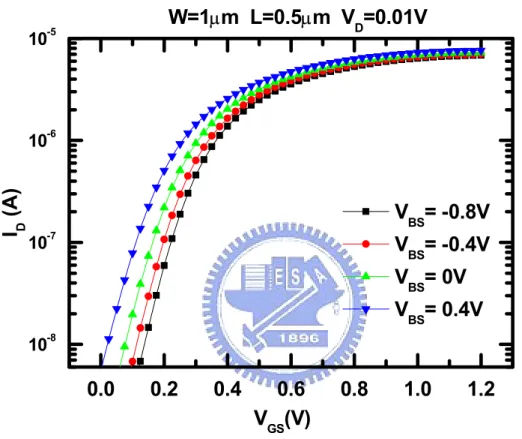
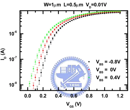
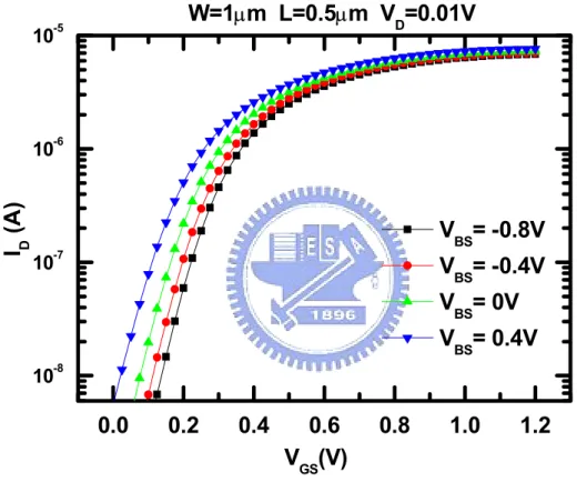
(19) gated lateral bipolar action as a new method for improving the matching.. 2.2 Experiment The measurement of current mismatch for identical devices was achieved in terms of the dies on wafer as schematically shown in Fig. 2.1. All dies on wafer contain many n-channel MOS transistors with the same structure. They were fabricated using a 65 nm CMOS process. In our measurement of current mismatch, the p-well-to-n+-source bias, VBS, was fixed when sweeping VGS from 0 to 1.2 V in a step of 25 mV. The drain currents were measured and recorded for subsequent analysis. This procedure was repeated for each VBS varying from 0.4 V to 0 V as well as from 0 V to -0.8 V. The choice for the maximum forward bias VBS of 0.4 V is to guarantee the action of the gated lateral bipolar transistor [7]-[9], as interpreted later. The measurement setup contained the HP4156B and a Faraday box for shielding the test wafer, all performed in an air-conditioned room with the temperature fixed at 298 K. The total measurement time of one die’s n-channel MOS for these full ranges was about 3 hours. A total of 25 sample size was measured in one die. Fig. 2.2 depicts typical measured I-V characteristic with VBS as a parameter from a single n-channel MOSFET. In Fig. 2.2 the operating regime of the interest in the work, i.e., weak. 8.
(20) inversion, is the range of VGS > 0 and ID < 10-8 ~10-7 A depending on the deviations from the exponential I-V relationship as will be clearly described later. The corresponding I-V curves are plotted in Fig. 2.3 for three different VBS values of 0.4, 0, and -0.8V. It is clearly seen from Fig. 2.3 that (i) the back-gate reverse bias causes a relatively large spread in the I-V characteristics; and (ii) for fixed VBS the spread decreases as the current increases. The statistical analysis of the our data in Fig. 2.3 is described in detail in next chapter.. 9.
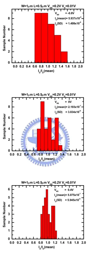
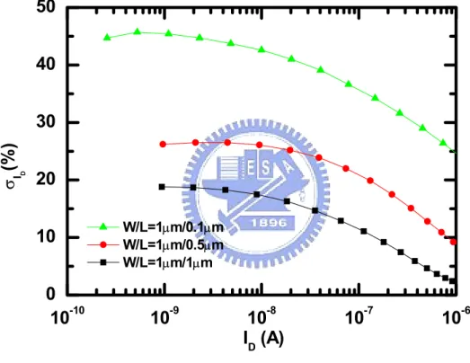
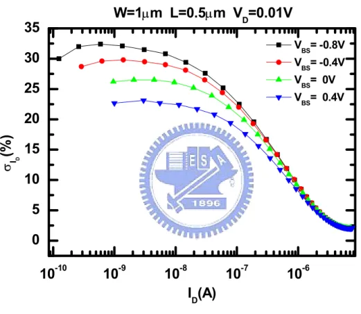
(21) Chapter 3 Dependence of Current Match on Back-Gate Bias 3.1 Analysis and Modeling The drain current mismatch σ ID is defined as σ ID = ID. (SD). / ID. (mean). where ID (mean) and ID (SD) are the mean and SD ( standard deviation ) of drain current for all the same dimensions of n-channel MOSFETs. We can calculate the mean and SD by means of a statistics tool. Fig. 3.1 shows the histogram of the drain current for different VBS as a parameter. From Fig. 3.1 we can observe that (i) for given VBS the distribution of ID; (ii) the distribution broadens as VBS varies from 0.4 V to -0.8 V. Fig. 3.2 shows the data in terms of σ ID versus ID for zero VBS, where W/L is the gate width to length ratio. In Fig. 3.2 our data from three dimensions are plotted for comparison. Further investigation of Fig. 3.2 reveals that the mismatch in weak inversion decreases with increasing the device area. However, this dependence must be scaled to account for process variations. Also from Fig. 3.2 it can be seen that, over all weak inversion current densities, the mismatch is essentially independent of current. In the moderate and strong inversion regions the mismatch significantly rolls off.. 10.
(22) The reasons for such dependencies are given in the following. In subthreshold the threshold voltage Vth affects exponentially the drain current ID through the following expression [1], [2], [4], [13]:. ID ∝ e. - kTq Vnth. (3.1). where Vth can be written as [13]:. Vth = VFB + 1.5φf + γ 1.5φf -VBS φf = γ=. kT N ln( A ) q ni t ox 2qε si N A. n = 1+. ε ox γ 2 1.5φf - VBS. where VFB is the flat-band voltage; NA is the effective well doping concentration; ni is the intrinsic concentration; tox is the oxide thickness; and εsi and εox are the silicon and oxide permittivities, respectively. According to (3.1), the variations in the fabrication process through NA, tox, and VFB cause a change in Vth, which in turn produces an exponential change in ID. However, in the above-threshold region the dependence of the drain current on the threshold voltage is turned to the well-know polynomial form, i.e.,. I D ∝ VDS (VGS -Vth ) or (VGS -Vth ) 2 11. (3.2).
(23) Therefore in the above-threshold region the variation in ID is a weak function of the variation in Vth as compared with the exponential change in weak inversion. The measured mismatch as a function of the bias VBS is given in Fig. 3.3. It is noted from Fig. 3.3 that in the weak inversion region the mismatch increases with increasingly negative VBS (from 0 V) and decreases with increasing the forward bias VBS. Such significant change is not as noticeable as the current enters the moderate and then strong inversion regions. This is because the corresponding dependence of drain current on the voltage changes from the exponential (3.1) to the polynomial (3.2). Note that a mathematical technique combining (3.1) and (3.2) as originally proposed in [14] can be utilized to empirically smooth the I-V characteristics of the transition region. Now we propose a new simple statistical model to quantitatively account for the above observed dependencies of the mismatch in weak inversion on the well-to-source bias. As revealed by (3.1), the our observed mismatch as a function of the VBS can be attributed to the variations in the oxide thickness tox, the doping concentration NA, and the flat-band voltage VFB. For simplifying the derivation, we consider the body effect γ, which contains tox and NA, as a single parameter responsible for the variations in. 12.
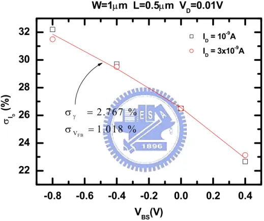
(24) both tox and NA. The variation in oxide charges and charged interface traps can essentially be reflected by the variation in the single parameter VFB. The validity of this procedure can be verified experimentally later. Assuming no correlation between parameters, from (3.1) the variance of the current different, σ ID , can be derived as function of both the variance of the difference in the body effect coefficient, σ γ , and the variance of the difference in the flat-band voltage, σ VFB , [15]:. σ 2ID ≅ (. V γ 2 ) (1.5φf -VBS )σ 2γ + ( FB ) 2 σ V2 FB nVT nVT. (3.3). where VT (=KT/q) is the thermal voltage. This new formulation explicitly describes the dependence of σ ID on VBS, i.e., the current mismatch increases with increasingly negative reverse bias VBS, while an increase in the forward bias VBS can improve the transistor matching. The calculated results based on (3.3) with σ γ = 2.767 % and σ VFB = 1.018 % have been found to be capable of appropriately reproducing the measured data as depicted in Fig. 3.4. The corresponding parameter values tox, VFB, and NA as provided by the experiment’s extract, which are also utilized later for identifying the regime of the gated lateral bipolar action in low level injection. From the above analysis and modeling, we can conclude that the mismatch becomes worse. 13.
(25) with the back-gate reverse bias applied and the current match can be substantially improved by slightly forward biasing the well-source junction.. 3.2 Detailed Interpretations Based on the above results, we suggest utilization of a MOS transistor with its well-to-source junction slightly forward biased or equivalently a gated n-p-n lateral bipolar transistor in low level injection [8]-[10] in order to improve the matching in the weak inversion region. Now we give interpretations for the action of the gated lateral bipolar transistor. Fig. 3.5 shows the drain current versus gate bias characteristics with forward bias VBS as parameter measured from one single n-channel MOSFET. According to our work [9]-[10], the measured I-V characteristics in Fig. 3.5 can be separated into two distinct regions: (i) the weak inversion region; and (ii) the strong inversion region. The condition for the surface inversion is VGS – VBS > Vth. Under this condition the opposite-polarity charges are induced at the surface beneath the gate and thus the drain current is dominated by drift component. The operating region of interest in this chapter is 0 < VGS < Vth + VBS. In this region the surface emitter(source)-base(well) junction barrier beneath the gate is lowered and almost all the injected electrons flowing toward the drain(acting as a. 14.
(26) collector) are limited to the surface depletion region [8]-[10], indicating that the pure bipolar collector current (which appears only for VGS < 0) is relatively negligible. The drain (or collector) current in the regime of 0 < Vth + VBS can be accurately described by [9]:. ID = I0e. q(ϕC +VBS ) kT. γ2 γ 2 ϕC = +(VGS -VBS -VFB )γ +4(VGS -VBS -VFB ) 2 2 where. φC. (3.4). represents the surface potential for lowering the emitter-base. junction barrier. In (3.4) the potential lowering is expressed as function of the process parameters such as the well doping concentration, the work function difference, and the gate oxide thickness as well as of the electrical parameters such as VGS and VBS. Note that the subthreshold current expression (3.3) can be derived from (3.4) using the Taylor series expansion [13]. Eq. (3.4) clearly reveals that the potential barrier can be lowered by the surface potential through the gate bias control, which causes an exponential change in the drain current. Note that the pure lateral bipolar action in a MOS transistor with well-to-source junction forward biased has also been reported in [11], [12] for improving the matching. However, the our operating condition and the mechanism responsible both are completely different from those in [11], [12]; 15.
(27) that is, in our work the pure lateral bipolar transistor action is relatively negligible since the surface carrier diffusion dominates the drain current, while in [11], [12] the pure lateral bipolar transistor action is totally responsible as cited there. Accurate comparisons can be presented in the following: (i) in [11], [12] the polarity of the VGS is negative while in our work it is positive; and (ii) in [11], [12] the pure lateral bipolar action occurs at VBS > 0.3 – 0.4 V while in our work the gated lateral bipolar action appears in low level regime of 0 V < VBS < 0.4V.. 3.3 Mismatch Model According to [15], the variance or standard deviation σg(x,y) of a function g(x,y) with two random variables x and y can be expressed as 2 σg(x,y) ≅ (. ∂g 2 2 ∂g ∂g ∂g ) σ x + ( ) 2 σ 2y + 2( )( )Cov (x,y) ∂x ∂y ∂x ∂y. (3.5). where σx and σy are the variances of x and y, respectively; and Cov(x,y) is the correlation coefficient between x and y. Thus the mismatch of the difference in the drain current ID can be written as function of the variances in the associated process parameters:. σ 2ID ≅ (. ∂V V γ 2 ∂Vth 2 2 ) ( ) σ γ + ( FB ) 2 ( th )σ 2VFB nVT ∂γ nVT ∂VFB. 16. (3.6).
(28) where σ ID , σ γ and σ VFB are the coefficient of variance of the difference in the ID, the body effect coefficient γ, and the flat-band voltage VFB, respectively. To facilitate the analysis, we assume Cov(VFB,γ) = 0. This is a basic assumption in the field [18]-[20] since the process variations are independent of each other in nature. Note that the variations in the gate oxide thickness tox and channel effective doping concentration NA are simultaneously reflected in the single parameter γ since γ includes both tox and NA, i.e. γ = tox 2qε si N A / εox where εsi and εox are the silicon and oxide permittivities, respectively. The following weak inversion current expression is considered for the derivation of the model [16]:. ID = A e. −. q Vth kT n. ln I D = ln A -. (3.7). 1 Vth VT n. where the critical voltage Vth = VFB + 1.5φf + γ 1.5φf -VBS ; the Fermi level φf =. γ kT N ln( A ) ; the slope n = 1 + ; and ni is the q ni 2 1.5φf - VBS. intrinsic concentration. From (3.7) the derivatives in (3.6) can easily be derived:. 17.
(29) ∂Vth = ∂γ. 1.5φf − VBS. (3.8). And. ∂Vth = 1 ∂VFB. (3.9). Thus we obtain a compact model:. σ ID ≅. (. γ 2 V ) (1.5φf -VBS )σ 2γ + ( FB ) 2 σ 2VFB nVT nVT. (3.10). Apparently, (3.10) analytically expresses the current mismatch in weak inversion as function of the coefficient of variance of the difference in VFB and γ. Fig. 3.6(a) shows four different gate width with the same length and Fig. 3.6(b) shows the same width with three different length for the coefficient of variance σ ID versus ID. Fig. 3.7 shows the measured drain current mismatch in weak inversion versus the back-gate bias with seven different dimensions. From Fig. 3.8(a) and (b) we can observe that the coefficient of variance in VFB and γ each effectively follow the inverse square root of the device area, in agreement with [18], [19]. Thus empirically we have. 18.
(30) σγ =. Aγ WL. and σ VFB =. A VFB WL. (3.11). where Aγ and A VFB are the size proportionality constants for σ γ and σ VFB , respectively. The extracted values lead to Aγ = 0.013464µm and A VFB = 0.006441µm. Therefore, a combination of (3.10) and (3.11) can serve as an analytic design tool for properly calculating the mismatch with back-gate forward bias and device size both as input parameters.. 19.
(31) Chapter 4 Conclusion. The current mismatch of a small gate area n-channel MOS transistor with its well-to-source junction forward and reverse biased has been extensively measured and analyzed. The n-channel MOS transistor with well-to-source junction slightly forward biased acts as a gated lateral bipolar transistor in low level injection. Our measured mismatch data for zero back-gate bias are close to the existing ones with comparable size. The measured data exhibit important observations: (i) back-gate reverse bias can make worse the mismatch in current; and (ii) current match can be substantially improved by the gated lateral bipolar action. The measured dependencies of the mismatch on the well-to-source forward and reverse biases have been successfully reproduced by a new simple statistical model. The new simple mismatch model has successfully reproduced the extensively measured data. The extracted variations in the associated process parameters have been found to follow the inverse square root of the device area. The work of optimizing the trade-off between the match and the device size with back-gate forward bias as design parameter has been demonstrated based on the model. 20.
(32) References. [1]. E. A. Vittoz, “Micropower techniques,” in Design of MOS VLSI. Circuits for Telecommunications, Y. Tsividis and P. Antognetti, Eds., Prentice-Hall, Inc., NJ. pp. 104-144, 1985. [2] A. Pavasovic, Subthreshold region MOSFET mismatch analysis and modeling for analog VLSI systems, Ph. D. Dissertation, the Johns Hopkins University, 1990. [3] F. Forti and M. E. Wright, “Measurement of MOS current mismatch in the weak inversion region,” IEEE J. Solid-State Circuits, vol. 29, pp. 138-142, Feb. 1994. [4] M. D. Godfrey, “CMOS device modeling for subthreshold circuit,” IEEE Trans. Circuits and Systems-II: Analog and Digital Processing, vol. 39. pp. 532-539, Aug. 1992. [5]. E. A. Vittoz, “The design of high-performance analog circuits on. digital CMOS chips,” IEEE J. Solid-State Circuits, vol. SC-20, pp. 657-655, June. 1985. [6]. L. Watts, D. A. Kerns, R. F. Lyon, and C. A. Mead, “Improved. implementation of the silicon cochlea,” IEEE J. Solid-State Circuits, vol. 27, pp. 692-700, May 1992. 21.
(33) [7] C.A. Mead Analog VLSI and Neural Systems, Addison-Wesley Co., MA., 1989. [8] S. Verdonckt-Vandebroed, S. S. Wong, J. C. S. Woo, and P. K. Ko “High-gain lateral bipolar action in a MOSFET structure,” IEEE Trans. Electron Devices, vol. 38, pp. 2487-2496, Nov. 1991. [9] T. H. Huang and M. J. Chen, “Empirical modeling for gate-controlled collector current of lateral bipolar transistors in an n-MOSFET structure,” Solid-State Electronics, vol. 38, pp. 115-119, Jan 1995. [10] T. H. . Huang and M. J. Chen, “Base current reversal phenomenon in a CMOS compatible high gain n-p-n gated lateral bipolar transistor,” IEEE Trans. Electron Devices, vol. 42, pp. 321-327, Feb. 1995. [11] E. A. Vittoz, “MOS transistors operated in the lateral bipolar mode and their application in CMOS technology,” IEEE J. Solid-State Circuits, vol. SC-18, pp. 273-279, June. 1983. [12] T. W. Pan and A. Abidi, “A 50-db variable gain amplifier using parasitic bipolar transistors in CMOS,” IEEE J. Solid-State Circuits, vol. 24, pp. 951-961, Aug 1989. [13]. Y. P. Tsividis, Operation and Modeling of the MOS Transistor,. McGraw-Hill Co., N.Y. 1987. [14] P. Antognetti, D Caviglia, and E. Profumo, “CAD model for threshold. 22.
(34) and subthreshold conduction in MOSFET’s,” IEEE J. Solid-State Circuits, vol. SC-17, pp. 454-458, June. 1982. [15] A. Papoulis, Probability, Random Variable and Stochastic Processes, Tokyo: McGraw-Hill, Kogakusha, 1965. [16] M. J. Chen, J. S. HO, and T. H. Huang, “Dependence of Current Match on Back-Gate Bias in Weakly Inverted MOS Transistors and Its Modeling,” IEEE J. Solid-State Circuits, vol. 31, pp. 259-262, Feb.1996. [17] E. A. Vittoz, “Low-power design: ways to approach the limits,” IEEE 1994 International Solid-State Circuits Conference, Digest of Technical Papers, pp. 14-18. [18]. K. R. Lakshmikumar, R. A. Hadaway, and M. A. Copeland,. “Characterization and modeling of mismatch in MOS transistors for precision analog design,” IEEE J. Solid-State Circuits, vol. 21, pp. 1057-1066, Dec. 1986. [19] M. J. M. Pelgrom, A. C. J. Duinmaijer, A. P. G. Welbers, “Matching properties of MOS transistors,” IEEE J. Solid-State Circuits, vol. 24, pp. 1433-1440, Oct. 1989. [20] C. Michael and M. Ismail, “Statistical modeling of device mismatch for analog MOS integrated circuit,” IEEE J. Solid-State Circuits, vol. 27, pp. 154-165, Feb.1992.. 23.
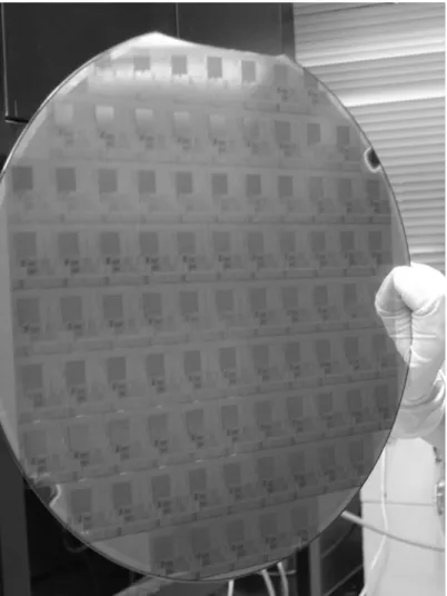
(35) Fig. 2.1. The used dies on wafer. All dies on wafer contain many n-channel MOS transistors with the same structure.. 24.
(36) W=1µm L=0.5µm VD=0.01V. -5. 10. -6. ID (A). 10. VBS= -0.8V -7. VBS= -0.4V. 10. VBS= 0V VBS= 0.4V -8. 10. 0.0. Fig. 2.2. 0.2. 0.4. 0.6 VGS(V). 0.8. 1.0. 1.2. The drain current versus gate voltage characteristics with back-gate bias as parameter from one of 25 n-channel MOSFETs in one die.. 25.
(37) W=1µm L=0.5µm VD=0.01V. -6. ID (A). 10. -7. 10. VBS = -0.8V VBS = 0V VBS = 0.4V. -8. 10. 0.0. 0.2. 0.4. 0.6. 0.8. 1.0. 1.2. VGS (V). Fig. 2.3 The measured drain current versus gate voltage characteristics for three different back-gate biases.. 26.
(38) W=1µm L=0.5µm VGS=0.2V VD=0.01V VBS. Sample Number. = -0.8V -8. 8. ID(mean)= 5.937x10 ID(SD). -8. = 1.499x10. 6 4 2 0 0.0 0.2 0.4 0.6 0.8 1.0 1.2 1.4 1.6 1.8 2.0 ID/ID(mean). W=1µm L=0.5µm VGS=0.2V VD=0.01V VBS. Sample Number. = 0V -7. 8. ID(mean)= 2.193x10 ID(SD). -8. = 3.834x10. 6 4 2 0 0.0 0.2 0.4 0.6 0.8 1.0 1.2 1.4 1.6 1.8 2.0 ID/ID(mean). W=1µm L=0.5µm VGS=0.2V VD=0.01V 6. VBS. = 0.4V -7. ID(mean)= 5.075x10. Sample Number. 5. ID(SD). -8. = 5.945x10. 4 3 2 1 0 0.0 0.2 0.4 0.6 0.8 1.0 1.2 1.4 1.6 1.8 2.0 ID/ID(mean). Fig. 3.1 The histogram for the NMOSFET dimension W/L = 1µm/0.5µm with three different VBS. 27.
(39) 50 40. D. σI (%). 30 20 10 0 -10 10. W/L=1µm/0.1µm W/L=1µm/0.5µm W/L=1µm/1µm -9. 10. -8. 10 ID (A). -7. 10. -6. 10. Fig. 3.2 The σ ID versus the drain current for zero back-gate bias.. 28.
(40) W=1µm L=0.5µm VD=0.01V. 35. VBS= -0.8V. 30. VBS= -0.4V VBS= 0V. 25. VBS= 0.4V. 15. D. σI (%). 20. 10 5 0 -10. 10. -9. 10. -8. -7. 10. 10. -6. 10. ID(A). Fig. 3.3 The measured drain current mismatch versus the drain current with the back-gate bias as parameter.. 29.
(41) W=1µm L=0.5µm VD=0.01V 32. -9. ID = 10 A -9. ID = 3x10 A. 30. D. σI (%). 28 σγ. 26. = 2.767 %. σ VFB = 1.018 %. 24 22 -0.8. -0.6. -0.4. -0.2. 0.0. 0.2. 0.4. VBS(V). Fig. 3.4 The measured drain current mismatch in weak inversion versus the back-gate bias for two different drain currents. The calculated results from Eq. (2.4) are also shown for comparison.. 30.
(42) W=1µm L=0.5µm VD=0.01V. -5. 10. -6. ID (A). 10. VBS= -0.8V. -7. 10. VBS= -0.4V VBS= 0V VBS= 0.4V. -8. 10. 0.0. Fig. 3.5. 0.2. 0.4. 0.6 VGS(V). 0.8. 1.0. 1.2. The drain current versus gate voltage characteristics with back-gate bias as parameter.. 31.
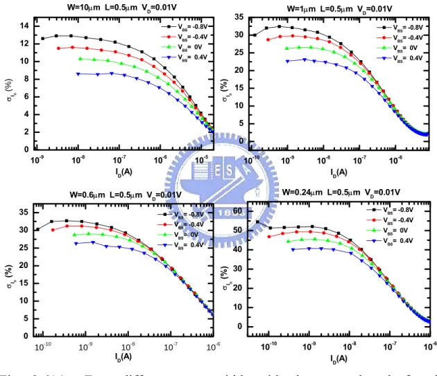
(43) W=10µm L=0.5µm VD=0.01V 14. VBS= -0.8V VBS= 0V. VBS= 0V VBS= 0.4V. 20. 8. σI (%). 6. 15. D. D. σI (%). VBS= -0.4V. 25. VBS= 0.4V. 10. VBS= -0.8V. 30. VBS= -0.4V. 12. W=1µm L=0.5µm VD=0.01V. 35. 4. 10 5. 2. 0. 0 -9. -8. 10. -7. 10. 10 ID(A). -6. -5. 10. -10. 10. -9. 10. 35. 10. -6. 10. W=0.24µm L=0.5µm VD=0.01V 60. VBS= -0.8V VBS= -0.4V. 30. VBS= -0.8V VBS= -0.4V. 50. VBS= 0V VBS= 0.4V. 25. VBS= 0V VBS= 0.4V. 40. 20. σI (%). 15. D. D. -7. 10. ID(A). W=0.6µm L=0.5µm VD=0.01V. σI (%). -8. 10. 10. 30 20 10. 5. 0. 0 10. -10. Fig. 3.6(a). 10. -9. -8. 10 ID(A). 10. -7. 10. -6. -10. 10. -9. 10. -8. 10 ID(A). -7. 10. -6. 10. Four different gate width with the same length for the coefficient of variance σ ID versus ID.. 32.
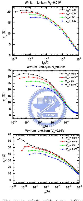
(44) W=1µm L=1µm VD=0.01V VBS= -0.8V. 20. VBS= -0.4V VBS= 0V VBS= 0.4V. D. σI (%). 15 10 5 0 -10. -9. 10. -8. 10. -7. -6. 10 10 ID(A) W=1µm L=0.5µm VD=0.01V. 35. 10. VBS= -0.8V. 30. VBS= -0.4V VBS= 0V. 25. VBS= 0.4V. 15. D. σI (%). 20. 10 5 0 -10. 10. -9. -8. 10. -7. 10. -6. 10. 10. ID(A). W=1um L=0.1um VD=0.01V. 70. VBS= -0.8V. 60. VBS= -0.4V VBS= 0V. D. σI (%). 50. VBS= 0.4V. 40 30 20 10 0 -11. 10. Fig. 3.6(b). -10. 10. -9. 10. -8. 10 ID(A). -7. 10. -6. 10. -5. 10. The same width with three different lengths for the coefficient of variance σ ID versus ID.. 33.
(45) D. σI (%). Area decreasing. 70 65 60 55 50 45 40 35 30 25 20 15 10 5. W0.24L0.1 µm W1L0.1 µm. W0.24L0.5 µm W1L0.5 µm. W10L0.1 µm W1L1 µm W10L0.5 µm. -0.8. -0.6. -0.4. -0.2 VBS(V). 0.0. 0.2. 0.4. Fig. 3.7 The measured drain current mismatch in weak inversion versus the back-gate bias with seven different dimensions.. 34.
(46) 5. σγ (%). 4 3 σγ =. 2. Αγ. WL Α γ =0.013464µm. 1. Experiment 0 0. 1. 2. 3. 4. 1/ WL (1/µm). Fig. 3.8(a) The measure and calculated σ γ versus the inverse square root of the device area.. 35.
(47) 3.0 2.5. FB. σV (%). 2.0 1.5 1.0. σ VFB =. WL A VFB =0.006441µm. 0.5 0.0. A VFB. Experiment 0. 1. 2. 3. 4. 5. 1/ WL (1/µm). Fig. 3.8(b) The measure and calculated σ VFB versus the inverse square root of the device area.. 36.
(48)
數據
+7
相關文件
Survivor bias is that when we choose a sample from a current population to draw inferences about a past population, we leave out members of the past population who are not in
By integrating data from a variety of government and commercial sources, we discovered 19,397 potential new commercial properties to inspect, based on the property usage types that
• The memory storage unit holds instructions and data for a running program.. • A bus is a group of wires that transfer data from one part to another (data,
• The memory storage unit holds instructions and data for a running program.. • A bus is a group of wires that transfer data from one part to another (data,
種植區內灌溉區如圖 2.所配置,一供水水源供水量充足,由兩個水閘門(閘門 A 及閘門 B)控制,以動力流供給渠道 A 及渠道 B,閘門 A 控制渠道 A 可供灌種 植區 0、2、4、6、8,閘門
As the result, I found that the trail I want can be got by using a plane for cutting the quadrangular pyramid, like the way to have a conic section from a cone.. I also found
3.16 Career-oriented studies provide courses alongside other school subjects and learning experiences in the senior secondary curriculum. They have been included in the
This paper presents (i) a review of item selection algorithms from Robbins–Monro to Fred Lord; (ii) the establishment of a large sample foundation for Fred Lord’s maximum
