高速低密度同位元檢查碼之解碼器設計
77
0
0
全文
(2) 高速低密度同位元檢查碼之解碼器設計 High-Throughput Low-Density Parity-Check Code Decoder Designs. 研 究 生:林凱立. Student:Kai-Li Lin. 指導教授:李鎮宜. Advisor:Chen-Yi Lee. 國 立 交 通 大 學 電子工程學系 電子研究所 碩士班 碩 士 論 文. A Thesis Submitted to Institute of Electronics College of Electrical Engineering and Computer Science National Chiao Tung University in Partial Fulfillment of the Requirements for the Degree of Master of Science in Electronics Engineering July 2005 Hsinchu, Taiwan, Republic of China. 中華民國九十四年七月.
(3) 高速低密度同位元檢查碼之解碼器設計. 學生:林凱立. 指導教授:李鎮宜 教授. 國立交通大學 電子工程學系 電子研究所碩士班. 摘要 在本論文中,我們提出了兩個高傳輸速度之低密度同位元檢查碼解碼器的設計。第 一個設計為應用於MB-OFDM UWB系統,區塊長度為 600 之解碼器。此架構採用了對 於通道資訊的資料流重新排程以及管線化來減低繞線上的擁擠程度和最長之延遲路 徑。經由 0.18µm製程實作晶片,我們所提出的此部份平行解碼器設計,於固定 8 次迴 圈的解碼模式下,可提供之最高資料傳輸速度為每秒 480Mb。第二個是基於區塊長度為 1200 之解碼器設計。為了達到更高的晶片密度及降低繞線上所造成的時間延遲,我們所 提出的架構採用了一個新的資料重新排序技術,將訊息記憶體和計算單元之間的資料匯 流排簡單化。經由此方法,由於晶片密度的提高,我們可大幅的縮減晶片的大小。另外, 此解碼器可同時處理兩筆不同之codeword來加快傳輸速度及資料路徑的工作效率。此設 計經由 0.18µm製程實作後,於晶片面積為 21.23mm2,固定 8 次迴圈的解碼模式下,其 最大資料傳輸速度可達到每秒 3.33Gb。另外,將此設計經由 0.13µm製程實作後,資料 傳輸速度可提升到每秒 5.92Gb,晶片面積縮小為 10.24mm2,而晶片之密度可提高至 75.4%。 i.
(4) High-Throughput Low-Density Parity-Check Code Decoder Designs. Student : Kai-Lin Lin. Advisor : Dr. Chen-Yi Lee. Department of Electronics Engineering Institute of Electronics National Chiao Tung University. ABSTRACT In this thesis, two high-throughput low-density parity-check (LDPC) code decoders are presented. The first one is a (600, 450) LDPC code decoder applied for MB-OFDM UWB applications. The architecture adopts a re-scheduling data flow for channel values and the pipeline structure to reduce routing congestion and critical path delay. After fabricated in 0.18µm 1P6M process, the proposed partially parallel decoder can support 480Mb/s data rate under 8 decoding iterations. Second decoder is implemented based on a (1200, 720) irregular parity check matrix. For achieving higher chip density and less interconnection delay, the proposed architecture features a new data reordering technique to simplify data bus between message memories and computational units; as a result, the chip size can be greatly reduced due to the increased chip density. Moreover, the LDPC decoder can also process two different codewords concurrently to increase throughput and datapath efficiency. After 0.18µm 1P6M chip implementation, a 3.33Gb/s data rate with 8 decoding iterations is achieved in the 21.23mm2 silicon area. The other experiment using 0.13µm 1P8M technology can further reach a 5.92Gb/s data rate within 10.24mm2 area while the chip density is 75.4%. ii.
(5) 誌. 謝. 隨著鳳凰花開,轉眼間又到了畢業的季節。在這二年的碩士生涯中,首先我要向指 導教授李鎮宜博士表達最誠摯的謝意。由於老師指導有方,讓我能在短時間內找到正確 的研究方向;在遇到挫折時也能從經驗中學習,培養正確的研究精神。另外,我也要感 謝 Si2 實驗室中的每一位成員。在這裡的每個人研究領域或有不同,但都願意彼此幫助, 讓我不僅了解團隊工作的重要性,更令人倍感溫馨;尤其我要感謝林建青學長,在我研 究過程中不厭其煩地提供不少建議。最後,我要謝謝在背後默默支持著我的家人和朋 友,讓我順利完成了這份學業。在大家的鼓勵下,讓我過得更多采多姿,我一定不會忘 記這段令人充滿回憶的生活。. iii.
(6) Contents CHAPTER 1 INTRODUCTION.............................................................................................1 1.1. MOTIVATION ................................................................................................................1. 1.2. THESIS ORGANIZATION ................................................................................................2. CHAPTER 2 LOW-DENSITY PARITY-CHECK CODES..................................................4 2.1. LDPC CODES ..............................................................................................................4. 2.2. MESSAGE PASSING ALGORITHM ..................................................................................7. 2.2.1. Principle of Message Passing Algorithm ...........................................................7. 2.2.2. Message Passing on Bit Nodes...........................................................................9. 2.2.3. Message Passing on Check Nodes ...................................................................10. 2.3. LDPC CODE DECODING ALGORITHM........................................................................12. 2.3.1. Sum-Product Algorithm (SPA) ..........................................................................12. 2.3.2. Log-Likelihood Ratio Sum-Product Algorithm (LLR-SPA) ..............................15. 2.3.3. Min-Sum Algorithm (MS) .................................................................................16. CHAPTER 3 HIGH-SPEED COMMUNICATION SYSTEMS WITH LDPC CODES .18 3.1. INTRODUCTIONS TO HIGH-SPEED COMMUNICATION SYSTEMS ..................................18. 3.1.1. Satellite Wireless Communication ....................................................................18. 3.1.2. 60GHz Band Wireless Communication ............................................................19. 3.1.3. Ultra-Wideband System ....................................................................................20 iv.
(7) 3.2. ERROR-CORRECTING PERFORMANCE OF LDPC CODES IN UWB SYSTEM ................22. 3.2.1. Performance Analysis of Code I .......................................................................23. 3.2.2. Performance Analysis of Code II......................................................................27. 3.2.3. Performance Comparison with Convolutional Codes......................................29. CHAPTER 4 ARCHITECTURES OF PROPOSED LDPC CODE DECODERS ...........31 4.1. INTRODUCTION TO THE CONVENTIONAL DESIGN .......................................................32. 4.2. PROPOSED LDPC CODE I DECODER DESIGN.............................................................34. 4.2.1. Channel Value Interconnection.........................................................................36. 4.2.2. Check Node Unit...............................................................................................38. 4.2.3. Bit Node Unit....................................................................................................42. 4.2.4. Chip Implementation ........................................................................................43. 4.3. PROPOSED LDPC CODE II DECODER DESIGN ...........................................................45. 4.3.1. Input Buffer.......................................................................................................46. 4.3.2. Check Node Unit and Bit Node Unit ................................................................50. 4.3.3. Message Memory Unit......................................................................................52. 4.3.4. Timing Schedule................................................................................................56. 4.3.5. Chip Implementation ........................................................................................57. 4.4. SUMMARY AND COMPARISON ....................................................................................60. CHAPTER 5 CONCLUSION AND FUTURE WORK.......................................................61 5.1. CONCLUSION .............................................................................................................61. 5.2. FUTURE WORK ..........................................................................................................61. BIBLIOGRAPHY...................................................................................................................62. v.
(8) List of Figures FIG. 2.1 EXAMPLE OF REGULAR LDPC CODE PARITY CHECK MATRIX ..........................................5 FIG. 2.2 BIPARTITE GRAPH OF THE CODE SPECIFIED BY MATRIX IN FIG. 2.1 ..................................6 FIG. 2.3 MESSAGE PASSING ON A NODE ........................................................................................8 FIG. 2.4 MESSAGE PASSING ON A BIT NODE ................................................................................10 FIG. 2.5 MESSAGE PASSING ON A CHECK NODE........................................................................... 11 FIG. 2.6 ITERATIVE DECODING FLOW CHART FOR LDPC CODES .................................................13 FIG. 2.7 MESSAGE PASSING IN LDPC CODE DECODING ..............................................................14 FIG. 3.1 FUNCTIONAL BLOCK DIAGRAM OF THE DVB-S.2 SYSTEM ............................................19 FIG. 3.2 BLOCK DIAGRAM OF MB-OFDM UWB SYSTEM .........................................................21 FIG. 3.3 BLOCK DIAGRAM OF THE PROPOSED LDPC-COFDM UWB SYSTEM ...........................22 FIG. 3.4 PERFORMANCE RESULTS OF THE (600, 450) LDPC CODE .............................................24 FIG. 3.5 FIXED POINT SIMULATION OF THE (600, 450) LDPC CODE ...........................................26 FIG. 3.6(A) BER OF THE (1200, 720) LDPC CODE ....................................................................27 FIG. 3.6(B) PER OF THE (1200, 720) LDPC CODE .....................................................................28 FIG. 3.7(A) FIXED POINT SIMULATION OF BER FOR THE (1200, 720) LDPC CODE ....................28 FIG. 3.7(B) FIXED POINT SIMULATION OF PER FOR THE (1200, 720) LDPC CODE .....................29 FIG. 3.8 PERFORMANCE COMPARISON FOR DIFFERENT CODES ....................................................30 FIG. 4.1 BLOCK DIAGRAM OF CONVENTIONAL LDPC CODE DECODER .......................................32 FIG. 4.2 ARCHITECTURE OF CONVENTIONAL CNU BASED ON: (A) LLR-SPA AND (B) MIN-SUM ALGORITHM .......................................................................................................................33. vi.
(9) FIG. 4.3 ARCHITECTURE OF CONVENTIONAL BNU.....................................................................34 FIG. 4.4 THE ARCHITECTURE OF LDPC CODE I DECODER..........................................................35 FIG. 4.5 THE PARTITION FOR PARITY CHECK MATRIX H OF CODE I..............................................36 FIG. 4.6 DATA PATH OF PROPOSED PARTIAL-PARALLEL DECODER................................................36 FIG. 4.7 PROPOSED LDPC DECODING FLOW ..............................................................................37 FIG. 4.8 TIMING DIAGRAM OF THE PROPOSED LDPC CODE I DECODER .....................................38 FIG. 4.9 BLOCK DIAGRAM OF CS14 ...........................................................................................39 FIG. 4.10(A) BLOCK DIAGRAM OF PROPOSED CMP-4 ................................................................40 FIG. 4.10(B) BLOCK DIAGRAM OF PROPOSED CMP-14...............................................................40 FIG. 4.11 THE PROPOSED 14-INPUT CNU ARCHITECTURE ..........................................................41 FIG. 4.12 THE PROPOSED BNU ARCHITECTURE .........................................................................43 FIG. 4.13 DIE MICROGRAPH OF THE LDPC-COFDM UWB TRANSCEIVER CHIP ........................44 FIG. 4.14 THE PARTITION OF PARITY CHECK MATRIX H OF CODE II ............................................45 FIG. 4.15 THE PROPOSED LDPC CODE II DECODER ARCHITECTURE ...........................................46 FIG. 4.16 THE CONVENTIONAL ARCHITECTURE OF INPUT BUFFER ..............................................47 FIG. 4.17(A) THE ARCHITECTURE OF RE BASED INPUT BUFFER ..................................................47 FIG. 4.17(B) THE TIMING DIAGRAM OF RE BASED INPUT BUFFER...............................................48 FIG. 4.18 THE ARCHITECTURE AND TIMING DIAGRAM OF RS-BASED INPUT BUFFER ...................49 FIG. 4.19 THE COMPARISON OF THREE INPUT BUFFER DESIGNS ..................................................50 FIG. 4.20 CNU ARCHITECTURE OF PROPOSED LDPC CODE II DECODER ...................................51 FIG. 4.21 BNU ARCHITECTURE OF PROPOSED LDPC CODE II DECODER ...................................51 FIG. 4.22 THE ARCHITECTURE AND TIMING DIAGRAM OF MUX-BASED MMU...........................52 FIG. 4.23(A) THE ARCHITECTURE OF RE-4B BASED MMU........................................................53 FIG. 4.23(B) THE TIMING DIAGRAM OF RE-4B BASED MMU.....................................................54 FIG. 4.24 THE ARCHITECTURE AND TIMING DIAGRAM OF RE-5B BASED MMU .........................55 FIG. 4.25 COMPARISON OF THREE MMU DESIGNS .....................................................................56 vii.
(10) FIG. 4.26 TIMING DIAGRAM OF PROPOSED LDPC CODE II DECODER .........................................57 FIG. 4.27 DIE MICROGRAPH OF THE 0.18µM LDPC CODE II DECODER CHIP...............................58 FIG. 4.28 LAYOUT VIEW OF THE 0.13µM LDPC CODE II DECODER CHIP ....................................59. viii.
(11) List of Tables TABLE 3.1 SPECIFICATION OF REFERENCED MB-OFDM UWB SYSTEM ....................................22 TABLE 3.2 BIT WIDTH DISTRIBUTION FOR DIFFERENT QUANTIZATION SCHEMES.........................25 TABLE 4.1 SUMMARY OF THE TWO LDPC CODES ......................................................................31 TABLE 4.2 COMPARISON OF DIFFERENT CNU ARCHITECTURES .................................................42 TABLE 4.3 SUMMARY OF THE LDPC CODE I CHIP .....................................................................44 TABLE 4.4 SUMMARY OF THE LDPC CODE II CHIP ....................................................................59 TABLE 4.5 COMPARISON OF LDPC CHIPS ..................................................................................60. ix.
(12) Chapter 1 Introduction 1.1. Motivation Low-density parity-check (LDPC) code, a linear block code defined by a very sparse. parity check matrix, was first introduced by Gallager [1], [2]. Due to the difficulty of circuit implementation, LDPC codes have been ignored for about forty years except for the study of codes defined on graphs by Tanner [3]. The rediscovery of LDPC codes were done by Spielman et al. [4] and MacKay et al. [5], [6]. It has engaged much research interest because the sparse property of parity check matrix makes the decoding algorithm simple and practical at good communication rates [5]. It was proven [7] that the LDPC code with large block length can beat turbo code [8], and achieve a capacity within 0.0045dB of the Shannon limit on AWGN channels. Besides their good error-correcting capability, LDPC codes have inherently fully parallelism and the simplicity of arithmetic computations. As a result, LDPC codes have been considered as next-generation forward error-control (FEC) technology for many high speed applications such as magnetic storage and telecommunications. However, the very large scale integrated circuits (VLSI) implementation of LDPC code decoders still remains a challenge in real applications. The main challenge of LDPC code decoder falls in the complex interconnections due to the randomness of parity check matrix. To efficiently design the decoder, the realization of its iterative decoding process which is referred to the message passing algorithm [5] becomes the most critical issue. According to different decoding schedules, the implementation of LDPC code decoders can be partitioned into two categories, fully parallel decoders and partially 1.
(13) parallel decoders. Fully parallel decoders directly map the corresponding bipartite graph [3] into hardware and all the processing units are hard-wired according to the connectivity of the graph. Thus they can achieve very high decoding speed but have a large hardware cost. The fully parallel implementation in [9] presents a 1024-bit, 1-Gb/s LDPC code decoder, which demands large area due to large amount of processing units and the complicated interconnections. The partially parallel architecture in [10] maps a certain number of processing unit into a single hardware block by using time-division multiplexing. It trades the decoding throughput for the reduction of hardware complexity. However, they also suffer from the same routing complications, and may be even worse due to multiplexers. Another implementation approach is presented in [11], which employs a turbo-like decoding algorithm with structured parity check matrices. The throughput is quite low due to the trellis-based decoding process. In this thesis, two decoders with different block lengths are implemented based on the partially parallel architecture. To solve the problems mentioned previously, efficient methods are proposed and applied to the decoders to eliminate multiplexers for less signal routing. The implementation results show how the proposed methods improve the performance. The detail discussion and architecture will be given in the following chapters.. 1.2. Thesis Organization The remainder of this thesis is organized as follows. Chapter 2 describes the. characteristics and decoding algorithms of LDPC codes. High-speed applications which adopted LDPC codes or potentially will adopt LDPC codes as the FEC kernel are introduced in Chapter 3. Simulation results and performance analysis will also be discussed here. In Chapter 4, the proposed LDPC code decoders, including functional units, data rescheduling and memory arrangement, are presented in detail. Besides, the chip implementation results 2.
(14) and comparisons with the state-of-the-arts will also be shown. Finally, conclusion and future work are made in Chapter 5.. 3.
(15) Chapter 2 Low-Density Parity-Check Codes Low-density parity-check (LDPC) codes are linear block codes that are specified by sparse parity check matrices containing mostly 0’s and only a small number of 1’s [1]. The code structures and decoding algorithms can be represented by bipartite graph [2]. Furthermore, it has been shown that the codes can achieve a capacity near Shannon limit with large block length. In this chapter, the code characteristics and decoding algorithms are presented.. 2.1. LDPC Codes The parity check matrix H which has N columns and M rows defines a LDPC code with. the block length of N bits and M parity checks. Assuming the matrix is of full rank, the number of information bits is K = N – M, and the code rate is R = 1 – M/N. It was shown by Gallager [2] that for large block lengths, the minimum distance of the code grows linearly with N. Thus block lengths of LDPC codes are often designed as large as possible. For a regular LDPC code, each column and row contains a fixed number of 1’s in H, leading to equal weights for both columns and rows. Otherwise, the code is termed irregular. It has been shown that irregular codes outperform regular codes due to wave effect [12]. An example of regular LDPC code parity check matrix is shown in Fig. 2.1. Generation a set of valid codewords requires the generator matrix G, which can be derived from H. The relationship between G and H can be expressed as. G⋅HT = 0 . 4. (2. 1).
(16) Let u = (u1 , u2 , u3 , ..., uK ) with u i = {0, 1} be the information bits, a LDPC code C is defined as. C = {x | x = u ⋅ G } .. (2. 2). Note that matrix G is not generally sparse; as a result, the complexity of encoding process is much higher due to the large and dense matrix multiplication. From equation (2.1) and (2.2), a valid codeword vector x = ( x1 , x2 , x3 , ..., xN ) should satisfy M parity check equations x ⋅ hi T = 0. i = 1, 2,..., M ,. (2. 3). where hi = (hi,1, hi,2, …, hi,N) denotes the row space of H.. 1 0 0 0 0. 1 0 0 0 0. 1 0 0 0 0. 1 0 0 0 0. 0 1 0 0 0. 0 1 0 0 0. 0 1 0 0 0. 0 1 0 0 0. 0 0 1 0 0. 0 0 1 0 0. 0 0 1 0 0. 0 0 1 0 0. 0 0 0 1 0. 0 0 0 1 0. 0 0 0 1 0. 0 0 0 1 0. 0 0 0 0 1. 0 0 0 0 1. 0 0 0 0 1. 0 0 0 0 1. 1 0 0 0 0. 0 1 0 0 0. 0 0 1 0 0. 0 0 0 1 0. 1 0 0 0 0. 0 1 0 0 0. 0 0 1 0 0. 0 0 0 0 1. 1 0 0 0 0. 0 1 0 0 0. 0 0 0 1 0. 0 0 0 0 1. 1 0 0 0 0. 0 0 1 0 0. 0 0 0 1 0. 0 0 0 0 1. 0 1 0 0 0. 0 0 1 0 0. 0 0 0 1 0. 0 0 0 0 1. 1 0 0 0 0. 0 1 0 0 0. 0 0 1 0 0. 0 0 0 1 0. 0 0 0 0 1. 1 0 0 0 0. 0 1 0 0 0. 0 0 1 0 0. 0 0 0 1 0. 0 0 0 0 1. 0 1 0 0 0. 1 0 0 0 0. 0 0 1 0 0. 0 0 0 1 0. 0 0 0 0 1. 0 1 0 0 0. 0 0 0 1 0. 1 0 0 0 0. 0 0 1 0 0. 0 0 0 0 1. Fig. 2.1 Example of regular LDPC code parity check matrix. LDPC codes can also be represented in bipartite graph. On one side the graph has N bit nodes which correspond to the N columns of H and M check nodes which correspond to the M rows of H on the other side. An edge which connects a bit node Bj and check node Ci corresponds to a 1 in the entry (i, j) of H. Fig. 2.2 is the corresponding bipartite graph of the LDPC code specified by the parity check matrix in Fig. 2.1. 5.
(17) B1. + + + + + +. C6. +. C7. +. C8. +. B8. C5. C9. +. B7. C4. C10. +. B6. C3. C11. +. B5. C2. C12. +. B4. C1. C13. +. B3. C14. +. B2. C15. B9. bit nodes. B10 B11 B12 B13 B14 B15 B16 B17 B18 B19 B20. check nodes. edge .. Fig. 2.2 Bipartite graph of the code specified by matrix in Fig. 2.1. 6.
(18) 2.2. Message Passing Algorithm In this section, message passing algorithm which is used to perform probabilistic. decoding is introduced. The intrinsic probability PEint ( x = a) represents the probability that the variable x chooses the value a. The extrinsic probability PEext ( x = a) describes the new information for variable x which is obtained from the event E. Moreover, the a posteriori probability PEpost ( x = a) represents the conditional probability that the variable x takes the value a based on the knowledge of event E.. 2.2.1. Principle of Message Passing Algorithm. The key factor of the message passing algorithm is to iteratively pass and exchange probabilistic messages in a graph. Extrinsic and a posteriori probabilities can be evaluated based on given intrinsic probabilities and the construction of the graph. Consider a node G with K+1 edges, which are associated with the variables e0, e1, …, eK belonging to the alphabet sets A0, A1, …, AK, respectively. The connection is shown as Fig. 2.3. For simplicity, only the case of binary variables is discussed in the following. That is, Ai ∈ Z 2 . Denote the intrinsic, extrinsic and a posteriori probability for ei with respect to event G as PGint (ei = ξi ) , PGext (ei = ξi ) and PGpost (ei = ξi ) , respectively. Assuming that the intrinsic probability for variable ei is available, the a posteriori probability can be derived by Bayes’ theorem as PGpost (ei = ξi ) = P(ei = ξi | G ) P (G, ei = ξi ) P(G ) 1 P(G | ei = ξi ) PGint (ei = ξi ). = P (G ) =. 7. (2.4).
(19) e1 e i-1. ei. G. ei+1. Pext(ei). ek. Fig. 2.3 Message passing on a node. Note that the extrinsic probability is in proportion to P (G | ei = ξi ) . That is PGext (ei = ξi ) = α i P (G | ei = ξi ) ,. (2.5). where α i is a scaling constant. A constraint set SG ∈ A0 × A1 × L × AK that the values of variables (e0, e1, …, eK) have to satisfy is defined on node G. Therefore, event G is true only when (ξ 0 , ξ1 ,..., ξ K ) ∈ SG ,. (2.6). where e0 = ξ 0 , e1 = ξ1 , ..., eK = ξ K . To evaluate the extrinsic and a posteriori probabilities of variables {ei }iK=0 , the probabilities of variable e0 are considered without loss of generality. Note that the product of alphabets A1 × A2 × … × AK forms a complete set of values for variables (e1, e2, …, eK). Hence,. ∑ ξ. (ξ1 ,...,. K. P({ei = ξi }iK=1 ) = 1 .. (2.7). )∈ A1 ×L × AK. In this way, the probability of event G can be decomposed as P (G ) =. ∑ ξ. (ξ1 ,...,. K. )∈ A1 ×L × AK. P(G, {ei = ξi }iK=1 ) .. (2.8). The extrinsic probability PGext (e0 = ξ 0 ) can thus be derived by PGext (e0 = ξ0 ) = α 0 P(G | e0 = ξ0 ) = α 0. ∑ ξ. (ξ1 ,...,. K )∈ A1 ×L × AK. P(G , {ei = ξi }iK=1 | e0 = ξ 0 ) ,. (2.9). where α 0 is a scaling constant. With chain rule and the independence of the variables {ei }iK=0 , the following result is obtained. 8.
(20) P (G, {ei = ξi }iK=1 | e0 = ξ0 ) = P(G |{ei = ξi }iK=0 ) ⋅ P({ei = ξi }iK=1 | e0 = ξ 0 ) K. = P (G |{ei = ξi }iK=0 ) ⋅ ∏ P(ei = ξi ) .. (2.10). i =1. Because event G is true only when equation (2.6) is satisfied, the first term in equation (2.10) can be written as ⎧1 if (ξ 0 , ξ1 ,..., ξ K ) ∈ SG P (G |{ei = ξi }iK=0 ) = ⎨ . otherwise ⎩0. (2.11). By putting together equation (2.9), (2.10) and (2.11), the expression of PGext (e0 = ξ 0 ) can be rewritten as PGext (e0 = ξ 0 ) = α 0. K. ∑ξ ξ. 1 ,..., K (ξ 0 ,ξ1 ,...,ξ K )∈SG. ∏P i =1. int G. (ei = ξi ) .. (2.12). The a posteriori probability PGpost (e0 = ξ 0 ) can be derived by combining equation (2.4) and (2.12). post G. P. ⎛ ⎞ K 1 ⎜ int (e0 = ξ0 ) = PG (ei = ξi ) ⎟ ⋅ PGint (e0 = ξ 0 ) ⋅ c0 ∑ ∏ ⎟ P(G ) ⎜⎜ ξ1 ,...,ξ K i =1 ⎟ ⎝ (ξ0 ,ξ1 ,...,ξ K )∈SG ⎠ = α 0′. ∑ξ ξ. K. ∏P. i =0 1 ,..., K (ξ0 ,ξ1 ,...,ξ K )∈SG. int G. (2.13). (ei = ξi ) ,. where α 0′ = α 0 ⋅1 P(G ) is a normalization constant.. 2.2.2. Message Passing on Bit Nodes. Representing one bit of the codeword, a bit node in a bipartite graph corresponds to a specified column in the parity check matrix H which defines the code. Thus the constraint on a bit node specifies that the associated variables should be equal. The constraint set SB on bit node B, which connects to K+1 check nodes, can be expressed as S B = {(e0 , e1 ,..., eK ) | e0 = e1 = L = eK } .. 9. (2.14).
(21) C0. C1. CK-1. CK. +. +. +. +. e1. e0. eK-1 e K. B Fig. 2.4 Message passing on a bit node. The connection is also shown in Fig. 2.4. For bit node B, the input message vector along edge ei is defined as µCi → B (ei ) , where i = 1~K. Based on equation (2.12) and (2.14), the output message µ B →C0 (e0 = ξ 0 ) along edge e0 is. µ B →C (e0 = ξ0 ) = PBext (e0 = ξ 0 ) 0. = α0. K. ∑. ∏µ. ξ1 ,...,ξ K i =1 (ξ0 ,ξ1 ,...,ξ K )∈S B. Ci → B. (ei = ξi ) .. (2.15). K. = α 0 ∏ µCi → B (ei = ξ0 ) , i =1. where α 0 is the normalization constant.. 2.2.3. Message Passing on Check Nodes. In a bipartite graph, a check node, denoting a parity check equation of the code, corresponds to a specified row in the parity check matrix H. Thus the constraint on a check node specifies that the summation of the associated bits should be zero. The constraint set SC on check node C, which connects to K+1 bit nodes, can be expressed as SC = {(e0 , e1 ,..., eK ) | e0 + e1 + L + eK = 0} ,. (2.16). where the operation “+” represents the modulo-2 summation. The connection is shown in Fig 2.5. 10.
(22) B0. B1. e0. BK-1. e1. eK-1. +. BK. eK. C. Fig. 2.5 Message passing on a check node. The input message vector along edge ei is denoted by µ Bi →C (ei ) for i = 1~K. With equation (2.12) and (2.15), the output message µC → B0 (e0 = ξ 0 ) along edge e0 can be derived as. µC → B (e0 = ξ0 ) = PCext (e0 = ξ 0 ) 0. = α 0′ = α 0′. K. ∑. ∏µ. ξ1 ,...,ξ K i =1 (ξ0 ,ξ1 ,...,ξ K )∈SC. ∑. ξ1 ,...,ξ K. Bi →C. (ei = ξi ). (2.17). K. [ξ0 + ξ1 + L + ξ K = 0]∏ µ Bi →C (ei = ξi ) , i =1. where [ξ 0 + ξ1 + L + ξ K = 0] is an indicator function that determines whether the parity check equation is satisfied. Because the indicator function consists of large number of possible configurations, the summation operation in equation (2.17) is very complicated. Thus we first consider the case of K=2 for simplicity. Therefore, 2 ⎡ ⎤ [0 ξ ξ 0] µ Bi →C (ei = ξi ) ⎥ + + = ∑ ∏ 1 2 ⎢ ⎡ µC → B0 (e0 = 0) ⎤ ξ1 ,ξ2 i =1 ⎥ . ⎢ ⎥=⎢ 2 ⎢ ⎥ = µ ( e 1) ⎢⎣ C → B0 0 ⎥⎦ ⎢ ∑ [1 + ξ1 + ξ 2 = 0]∏ µ Bi →C (ei = ξi ) ⎥ ⎢⎣ξ1 ,ξ2 ⎥⎦ i =1. (2.18). When e0 = 0, the indicator function is true if and only if the configuration is either e1 = e2 = 0 or e1 = e2 = 1. Hence equation (2.18) can be decomposed as. 11.
(23) ⎡ µC → B0 (e0 = 0) ⎤ ⎡ µ B1 →C (e1 = 0) µ B2 →C (e2 = 0) + µ B1 →C (e1 = 1) µ B2 →C (e2 = 1) ⎤ ⎢ ⎥=⎢ ⎥ ⎢⎣ µC → B0 (e0 = 1) ⎥⎦ ⎢⎣ µ B1 →C (e1 = 0) µ B2 →C (e2 = 1) + µ B1 →C (e1 = 1) µ B2 →C (e2 = 0) ⎥⎦. ( (. )( ). ). ⎡ 1 − µ B →C (e1 = 1) 1 − µ B →C (e2 = 1) + µ B →C (e1 = 1) µ B →C (e2 = 1) ⎤ 1 2 1 2 ⎥, =⎢ ⎢ 1− µ ⎥ B1 →C (e1 = 1) µ B2 →C (e2 = 1) + µ B1 →C (e1 = 1) 1 − µ B2 →C (e2 = 1) ⎦ ⎣. (. ). (2.19) where µ B1 →C (e1 = 0) = 1 − µ B1 →C (e1 = 1) and µ B2 →C (e2 = 0) = 1 − µ B2 →C (e2 = 1) . Furthermore, the expression in equation (2.19) can be rewritten as. (. )( )(. ) ⎤⎥ . )⎥⎦. ⎡ 2 µC → B0 (e0 = 0) − 1⎤ ⎡ 1 − 2 µ B1 →C (e1 = 1) 1 − 2 µ B2 →C (e2 = 1) ⎢ ⎥=⎢ 2 µ ( e 1) 1 = − ⎢⎣ C → B0 0 ⎥⎦ ⎢⎣ − 1 − 2 µ B1 →C (e1 = 1) 1 − 2µ B2 →C (e2 = 1). (. (2.20). By induction [13], the results in equation (2.20) can be generalized for K>2 and becomes ⎡ K 1 − 2µ Bi →C (ei = 1) ⎡ 2µC → B0 (e0 = 0) − 1⎤ ⎢ ∏ i =1 ⎢ ⎥=⎢ K = − 2 µ ( e 1) 1 ⎣⎢ C → B0 0 ⎦⎥ ⎢ − ⎢ ∏ 1 − 2 µ Bi →C (ei = 1) ⎣ i =1. (. (. ) ⎤⎥ ). ⎥ . ⎥ ⎥ ⎦. (2.21). As a result, the output messages can be expressed in terms of the input messages: K ⎡1 ⎤ (1 (1 − 2 µ Bi →C (ei = 1))) ⎥ + ∏ ⎢ µ e ( 0) = ⎡ C → B0 0 ⎤ 2 i =1 ⎥ . ⎢ ⎥=⎢ K ⎥ ⎢⎣ µC → B0 (e0 = 1) ⎥⎦ ⎢ 1 (1 − (1 − 2µ ∏ ⎢ Bi →C (ei = 1))) ⎥ i =1 ⎣2 ⎦. 2.3. LDPC Code Decoding Algorithm. 2.3.1. Sum-Product Algorithm (SPA). (2.22). For a M × N parity check matrix H and the corresponding graph, Bi for i = 1, 2, …, N denote the bit nodes, Cj for j = 1, 2, …, M are check nodes, and eij is the edge connecting Bi and Cj. Furthermore, M(i) is the set of check nodes connected to bit node Bi, and L(j) is the set of bit nodes that are associated with check node Cj. The codeword is also represented by x = [ x1 , x2 ,L , xN ] . The intrinsic probabilities with respect to the LDPC code can thus be 12.
(24) written as int PLDPC ( xi ) = P ( xi = ξi ) ,. (2.23). where ξi ∈ {0, 1} and P ( xi = 0) = 1 − P ( xi = 1) , assuming binary symmetric channel. Fig 2.6 illustrates the iterative decoding flow of LDPC codes where each step will be described as follows [5].. Initialization. Horizontal Step. Iterative Decoding. No. Vertical Step. Syndrome Check. Yes. Output Estimated Bits. Fig. 2.6 Iterative decoding flow chart for LDPC codes. (1) Initialization: The messages from bit node Bi to check node Cj are initialized as ⎡ µ Bi →CJ (eij = 0) ⎤ ⎡ P( xi = 0) ⎤ ⎢ ⎥=⎢ ⎥ . ⎣⎢ µ Bi →CJ (eij = 1) ⎥⎦ ⎣ P( xi = 1) ⎦. (2.24). (2) Horizontal step: As shown in Fig. 2.7(a), message updates associated with check nodes are completed in this step. As shown in equation (2.22), the update equations can be expressed as ⎡1 ⎤ (1 + ∏ (1 − 2µ Bi′ →C j (ei′j = 1))) ⎥ ⎢ ⎡ µC j → Bi (eij = 0) ⎤ 2 Bi′ ∈L ( j )\ Bi ⎥ , ⎢ ⎥=⎢ ⎢ ⎥ = µ e ( 1) 1 ⎢⎣ C j → Bi ij ⎥⎦ ⎢ (1 − ∏ (1 − 2 µ Bi′ →C j (ei′j = 1))) ⎥ ⎢⎣ 2 ⎥⎦ Bi′ ∈L ( j )\ Bi. (2.25). where L(j)\Bi is the set of bit nodes that participate in check node Cj except Bi.. (3) Vertical step: In vertical step, the messages associated with bit nodes are updated as illustrated in Fig. 2.7(b). According to equation (2.15), the update equations can be 13.
(25) expressed as. ⎡α ij P( xi = 0) ∏ µC j′ → Bi (eij′ = 0) ⎤ ⎡ µ Bi →C j (eij = 0) ⎤ ⎢ ⎥ C j′ ∈M ( i )\ C j ⎢ ⎥=⎢ ⎥ , ⎢⎣ µ Bi →C j (eij = 1) ⎦⎥ ⎢ α ij P( xi = 1) ∏ µC j′ → Bi (eij′ = 1) ⎥ C j′ ∈M ( i )\ C j ⎥⎦ ⎣⎢. (2.26). where M(i)\Cj is the set of check nodes that connect to bit node Bi except Cj and α ij is chosen such that µ Bi →C j (eij = 0) + µ Bi →C j (eij = 1) = 1 .. (4) Syndrome check: The a posteriori probabilities for each codeword bit can be computed as ⎡α i P( xi = 0) ∏ µC j → Bi (eij = 0) ⎤ ⎡ P post ( xi = 0) ⎤ ⎢ ⎥ C j ∈M ( i ) ⎢ post ⎥=⎢ ⎥ , ⎣⎢ P ( xi = 1) ⎦⎥ ⎢ α i P( xi = 1) ∏ µC j → Bi (eij = 1) ⎥ C j ∈M ( i ) ⎥⎦ ⎣⎢. (2.27). where normalization factor α i is used to ensure P post ( xi = 0) + P post ( xi = 1) = 1 . The estimated bit xˆi is set to 1 if P post ( xi = 1) > 0.5 , otherwise it is set to 0. Then the syndrome equation. xˆ H T = 0. is verified whether the estimated sequence. xˆ = [xˆ1 , xˆ2 ,L , xˆ N ] is a valid codeword.. The decoding process halts when the syndrome check equation is satisfied; otherwise it goes into the next decoding iteration. A failure is declared if some maximum number of iterations occurs without finding a valid codeword.. Bi. Bi. P(xi = ξi). L(j) +. +. Cj. (a) Horizontal step. +. +. (b) Vertical step. Fig. 2.7 Message passing in LDPC code decoding 14. M(i) +.
(26) 2.3.2. Log-Likelihood Ratio Sum-Product Algorithm (LLR-SPA). For a binary codeword, the decoding operations can be performed in terms of log-likelihood ratios [15]. The log-likelihood ratio (LLR) of a random variable U can be defined as L(U ) = log. P(U = 0) . P (U = 1). (2.28). Therefore, the decoding flow can be modified as follows.. (1) Initialization: The messages sent from bit node Bi to check node Cj are initialized by LBi →C j (eij ) = log. P( xi = 0) , P( xi = 1). (2.29). which is the so-called “channel value” or “channel information”.. (2) Horizontal step: Based on equation (2.25), the update operation in logarithmic domain can be rewritten as LC j → Bi (eij ) = log. µC → B (eij = 0) j. i. µC → B (eij = 1) j. 1+ = log. i. (1 − 2µ ∏ (1 − 2µ ∏. Bi′ ∈L ( j )\ Bi. 1−. Bi′ ∈L ( j )\ Bi. ) . = 1) ). Bi′ →C j. (ei′j = 1). Bi′ →C j. (ei′j. (2.30). Based on the hyperbolic tangent function and the arc-hyperbolic tangent function, u eu − 1 tanh( ) = u 2 e +1. and tanh −1 ( y ) =. 1 1+ y , log 2 1− y. (2.31). the term 1 − 2µ Bi′ →C j (ei′j = 1) in equation (2.31) can be expressed as ⎛1 ⎞ 1 − 2µ Bi′ →C j (ei′j = 1) = tanh ⎜ LBi′ →C j (ei′j ) ⎟ . ⎝2 ⎠ Combining (2.30), (2.31) and (2.32), we can derive. 15. (2.32).
(27) ⎛1 ⎞ tanh ⎜ LBi′ →C j (ei′j ) ⎟ 2 ⎝ ⎠ Bi′ ∈L ( j )\ Bi LC j → Bi (eij ) = log ⎛1 ⎞ 1 − ∏ tanh ⎜ LBi′ →C j (ei′j ) ⎟ ⎝2 ⎠ Bi′ ∈L ( j )\ Bi. ∏. 1+. (2.33). ⎛ ⎛1 ⎞⎞ = 2 tanh −1 ⎜⎜ ∏ tanh ⎜ LBi′ →C j (ei′j ) ⎟ ⎟⎟ . ⎝2 ⎠⎠ ⎝ Bi′∈L ( j )\ Bi. (3) Vertical step: Using LLR, the update equation can be rewritten as LBi →C j (eij ) = log. µ B →C (eij = 0) i. j. µ B →C (eij = 1) i. j. α ij P( xi = 0) = log. α ij P( xi = 1). = L( xi ) +. ∑. ∏. µC. j′ → Bi. ∏. µC. (eij′ = 1) j′ → Bi. C j′ ∈M ( i )\ C j. C j′ ∈M ( i )\ C j. C j′ ∈M ( i )\ C j. (eij′ = 0) (2.34). LC j′ → Bi (eij′ ) ,. where L(xi) is the intrinsic log-likelihood ratio of bit xi.. (4) Syndrome check: The pseudo- a posteriori probabilities for each codeword bit can be computed as post. L. P post ( xi = 0) ( xi ) = log post P ( xi = 1) = L( xi ) +. ∑. C j ∈M ( i ). (2.35). LC j → Bi (eij ) .. Hard decision are performed based on the sign of Lpost ( xi ) ; therefore, bit xˆi is set to 1 if Lpost ( xi ) is negative, otherwise it is set to 0. Compared with the SPA, multiplications are replaced by additions and the normalization factors are eliminated in the LLR-SPA. Less complexity in implementation is achieved when LLR-SPA is employed.. 2.3.3. Min-Sum Algorithm (MS). In the LLR-SPA, the horizontal step is the most computationally complex part because of hyperbolic tangent functions. Hence it is difficult to implement in hardware based on 16.
(28) LLR-SPA. To further simplify the decoding process, the min-sum algorithm [16] is introduced. We first consider a check node with 3 edges without loss of generality. Combining equation (2.20), (2.31) and (2.32), we can obtain ⎛ e LB1→C ( e1 ) − 1 e LB2→C ( e2 ) − 1 ⎞ 1 + ⎜⎜ LB →C ( e1 ) ⋅ LB →C ( e2 ) ⎟⎟ 1 e + 1 e 2 +1 ⎠ LC → B0 (e0 ) = log ⎝ L ( e ) L ( e ) ⎛ e B1→C 1 − 1 e B2 →C 2 − 1 ⎞ ⋅ L (e ) 1 − ⎜⎜ LB →C ( e1 ) ⎟ 1 + 1 e B2→C 2 + 1 ⎠⎟ ⎝e = log. 1+ e e. LB1→C ( e1 ) LB2 →C ( e2 ). e. LB1→C ( e1 ). +e. (2.36). .. LB2 →C ( e2 ). Based on the approximation in [17], equation (2.36) becomes. (. LC → B0 (e0 ) = log 1 + e. LB1→C ( e1 ) + LB2 →C ( e2 ). ) − log ( e. LB1→C ( e1 ). +e. (. ) − max ( L (e ), L (e ) ) − log(1 + e = sign ( L (e ) ) sign ( L (e ) ) min ( L ≈ sign ( L (e ) ) sign ( L (e ) ) min ( L. = max 0, LB1 →C (e1 ) + LB2 →C (e2 ) + log(1 + e B1 →C. 1. B2 →C. 2. LB2 →C ( e2 ). ). − LB1→C ( e1 ) + LB2 →C ( e2 ). − LB1→C ( e1 ) − LB2 →C ( e2 ). ). ). (2.37). ) (e ) ). B1 →C. 1. B2 →C. 2. B1 →C. (e1 ) , LB2 →C (e2 ) + g (e1 , e2 ). B1 →C. 1. B2 →C. 2. B1 →C. (e1 ) , LB2 →C. where g (e1 , e2 ) = log(1 + e. − LB1→C ( e1 ) + LB2 →C ( e2 ). ) − log(1 + e. − LB1→C ( e1 ) − LB2 →C ( e2 ). 2. ,. ) is the correction factor.. By induction [15], the result in equation (2.37) can be generalized to obtain a sub-optimal expression of the horizontal step, which is. ⎛ LC j → Bi (eij ) ≈ ⎜⎜ ∏ sign LBi′ →C j (ei′j ) ⎝ Bi′∈L ( j )\ Bi. (. ⎞. ) ⎟⎟. ⎠. min. Bi′ ∈L ( j )\ Bi. (L. Bi′ →C j. (ei′j ). ). .. (2.38). This approximation results in a significant reduction of hardware complexity but little penalty of degraded performance [18]. In the min-sum algorithm, all steps of the decoding are the same with LLR-SPA except for the horizontal step. Thus the min-sum algorithm can be derived by just replacing equation (2.33) with (2.38) in LLR-SPA. 17.
(29) Chapter 3 High-Speed Communication Systems with LDPC Codes In communication systems, channel coding is a key technique to minimize the interferences from the noisy channel. Due to the excellent error-correcting ability and the inherent parallelism, LDPC codes are suitable for high-speed applications. In this chapter, high-speed communication systems that adopted LDPC codes or potentially will apply LDPC codes as the channel coding technology are introduced. The simulation results of the error-correcting performance are also shown in the following.. 3.1. Introductions to High-Speed Communication Systems. 3.1.1. Satellite Wireless Communication. Digital video broadcasting (DVB) standards are established to deliver videos for the subscriber to provide various entertainments. Over past few years, different broadcasting modes have been designed for kinds of purposes, including the terrestrial, cable and satellite broadcasts. The original satellite digital video broadcasting (DVB-S) was developed in 1994 [19], whose forward error correction (FEC) technology is the concatenation of convolutional codes and Reed-Solomon codes. It is now used worldwide by most of the satellite operators for data and television broadcasting services. To improve the overall performance of the digital satellite transmission technology, the second generation of DVB-S (DVB-S.2) was developed [20]. As a successor to the current DVB-S standard, DVB-S.2 is expected to 18.
(30) provide not only existing but also new services, including TV, High Definition Television (HDTV), audio and other multimedia services. Employing a powerful FEC system based on LDPC codes concatenated with BCH codes, DVB-S.2 allows quasi-error-free (QEF) operation at about 0.7dB to 1.0dB from the Shannon limit, depending on the transmission mode [20]. Moreover, a capacity gain in the order of 30 percent over DVB-S is achieved due to higher order modulation schemes. The functional block diagram of the DVB-S.2 system is illustrated in Fig. 3.1.. FEC TX Data. Mode Adaptation. Stream Adaption. RF. BCH Encoder. Modulation. LDPC Encoder. PL Framing. Bit Interleaver. Mapping. Fig. 3.1 Functional block diagram of the DVB-S.2 system. To transmit data via satellite, DVB-S.2 targets for a robust and reliable communication service. The corresponding packet error rate for DVB-S.2 at QEF over AWGN channel is 10-7, which is very low as compared to other systems. Therefore LDPC codes with large block lengths, which are 64,800 and 16,200, are chosen to accomplish excellent error performance. And different coding rate of LDPC codes are specified to accommodate various transmission modes.. 3.1.2. 60GHz Band Wireless Communication. Recently, the Federal Communications Commission (FCC) released the RF band around 60GHz, leading to a new era in the millimeter wave based communications. It potentially can 19.
(31) provide a variety of applications including high-speed wireless personal area network (WPAN), automotive radar at nearby frequencies and multimedia communications. The corresponding standardization (IEEE 802.15.3c) is now under construction by IEEE 802.15 Working Group for WPANs. It is intended to offer higher data transmission, higher frequency re-usage and superior coexistence than the existing wireless systems. The working group also suggest IEEE 802.15.3c will be widely used for Gigabit Ethernet and replace the cables and other wired links. One of the optional data rate suggested by IEEE 802.15.3c is greater than 2Gb/s in order to satisfy an evolutionary set of consumer multimedia industry in WPAN communications. Due to the required high data rate, LDPC codes are potential candidates for the FEC technique. With parallel implementation, the LDPC code decoders can easily achieve the demands for data rates over Gb/s.. 3.1.3. Ultra-Wideband System. Ultra-wideband (UWB) is an emerging wireless physical (PHY)-layer technology that uses a very large bandwidth [21], [22]. It possesses unique advantages that are attractive to the communication applications: i) the potential for very high data throughput and large increase in user capacity; ii) the implementation of UWB potentially takes small size and processing power; and iii) ultra high precision ranging at centimeter level [22]. Due to the lack of available spectral bands, the applications of UWB devices prior to 2001 were mainly for military usage. In the spring of 2002, the FCC unleashed 3.1GHz to 10.6GHz RF band for increasing high-speed data transmission. Responding to this FCC ruling, industries, government agencies and academic institutions made many research efforts that adopted UWB technology in various areas. These include short-range high-speed wireless communication, localization system, high-resolution radar and imaging system. In this thesis, 20.
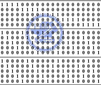
(32) we will focus on the UWB applications for wireless networks. UWB addresses short-range connections among digital home electronics appliances that are applied for the wireless personal area network (WPAN). It is expected to provide high-speed data exchange among storage systems and real-time video/audio distribution for home entertainment devices. Due to small power consumption and high data rate, UWB technology will be exploited to replace existing wireless services. In [23], the multi-band orthogonal frequency-division multiplexing (MB-OFDM) PHY-layer proposal indicates the coded OFDM based solution can provide up to 480Mb/s for 528MHz UWB system. The desired range in MB-OFDM is 10m for 110Mb/s and can be reduced for higher data rates [23]. To enhance the overall system performance, the convolutional codes and interleaving techniques are applied in the FEC mechanism, whose block diagram is shown in Fig. 3.2.. Baseband TX Data. Scrambler. Convolutional Encoder. Interleaver. OFDM Modulator. DAC. RF. RX Data. De-Scrambler. Viterbi Decoder. De-Interleaver. OFDM De-Modulator. ADC. RF. Fig. 3.2 Block diagram of MB-OFDM UWB system. For improving PHY-layer capacity, LDPC codes can increase the throughput to over 500Mb/s in future WLAN applications [24]. And the LDPC coded OFDM baseband system has been silicon proven to achieve 480 Mb/s data rate [25]. To provide better performance, the original convolutional codes and bit interleaving are replaced with LDPC codes in MB-OFDM UWB systems [25] as shown in Fig. 3.3. The overall system performance will be 21.
(33) described and discussed later.. Baseband TX Data. Scrambler. LDPC Encoder. OFDM Modulater. DAC. RF. RX Data. De-Scrambler. LDPC Decoder. OFDM De-Modulater. ADC. RF. Fig. 3.3 Block diagram of the proposed LDPC-COFDM UWB system. 3.2. Error-Correcting Performance of LDPC Codes in UWB System In the MB-OFDM UWB systems [25], the maximum 480Mb/s data rate with a. bandwidth of 528MHz is specified. The time domain spreading scheme is used to change the data rate for different channel state information. In the following, the simulation results are based on the system illustrated in Fig 3.3, whose detail specification is given in Table 3.1. Two different irregular LDPC codes are constructed by the progressive edge-growth (PEG) algorithm [26] to enhance the system performances. One is (600, 450) LDPC code (Code I), and the other is (1200, 720) LDPC code (Code II).. Table 3.1 Specification of referenced MB-OFDM UWB system. Data rate (Mb/s). 120. 240. 480. Spreading gain. 4. 2. 1. QPSK. Constellation 22.
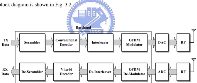
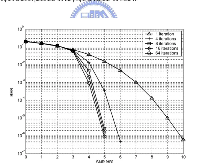
(34) Data carrier. 100. FFT size. 128. Packet size (Bytes). 1024. Signal bandwidth (MHz). 528. Channel model. Additive White Gaussian Noise (AWGN). As stated in Chapter 2, the pseudo- a posteriori probabilities of the codeword bits gradually converge to the real a posteriori probabilities as the number of decoding iterations grows. And the internal messages which are exchanged between check nodes and bit nodes are soft values. However, since infinite decoding iterations and infinite signal precision are impossible for practical implementation, the maximum iteration number and the quantization bits have to be decided. Some performance degradation would be introduced due to the implementation limitations. As a result, a trade-off between the performance and hardware cost will be concerned in the following.. 3.2.1. Performance Analysis of Code I. Code I is a (600, 450) rate-3/4 irregular LDPC code, whose column weights are fixed to 3 and row weights are ranging from 11 to 14. Based on the referenced MB-OFDM UWB system, its performances with different decoding iterations including the bit-error rate (BER) and packet-error rate (PER), which is demanded to be less than 8% [21], is shown in Fig 3.4.. 23.
(35) 10. 10. 10. 1 iteration 4 iterations 8 iterations 16 iterations 64 iterations. -1. -2. -3. BER. 10. 0. 10. 10. 10. 10. 10. PER. 10. 10. 10. 10. -4. -5. -6. -7. 0. 1. 2. 3. 4. 5 SNR [dB] (a). 6. 7. 8. 9. 10. 0. -1. -2. -3. 1 iteration 4 iterations 8 iterations 16 iterations 64 iterations PER=8%. -4. 0. 1. 2. 3. 4. 5 SNR [dB] (b). 6. 7. 8. Fig. 3.4 Performance results of the (600, 450) LDPC code 24. 9. 10.
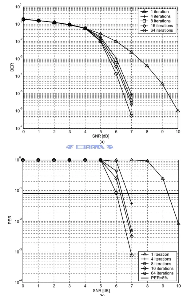
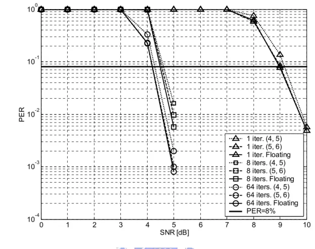
(36) Note that the required signal to noise ratio (SNR) is reduced as the iteration number increases. In Fig. 3.4(b), 3dB SNR gain at PER = 8% is achieved as the number of decoding iterations moves from 1 to 8. However, the improvement tends to be insignificant after 8 iterations, which is only about 0.3dB. As a result, LDPC decoding for Code I with 8 iterations in referenced MB-OFDM UWB system is considerably a good trade-off for practical implementation. Quantization has to be performed for two types of signal values. One is the channel values, and the other is the internal messages. Fig. 3.5 shows the fixed point simulation results of Code I, where the notation (p, q) represents that the bit width of channel values and internal messages are p and q bits, respectively. The number of bits used for the integer and the fractional part in each (p, q) quantization schemes are shown as Table 3.2.. Table 3.2 Bit width distribution for different quantization schemes. Quantization scheme. Channel value. Internal message. Integer part. Fractional part. Integer part. Fractional part. (4, 5). 1. 3. 1. 4. (5, 6). 1. 4. 1. 5. Many combinations of the quantization schemes and the bit width distributions have been tested through simulations. The performances of the quantization with more precision than (5, 6) scheme are almost the same as those with infinite precision. Consequently, the (5, 6) scheme together with the bit width distribution listed in Table 3.2 are used for the proposed LDPC Code I decoder.. 25.
(37) 10. 10. BER. 10. 10. 10. 10. 10. 10. 10. PER. 10. 10. 10. 10. 0. 1 iter. (4, 5) 1 iter. (5, 6) 1 iter. Floating 8 iters. (4, 5) 8 iters. (5, 6) 8 iters. Floating 64 iters. (4, 5) 64 iters. (5, 6) 64 iters. Floating. -1. -2. -3. -4. -5. -6. -7. 0. 1. 2. 3. 4. 5 SNR [dB] (a). 6. 7. 8. 9. 10. 0. -1. -2. 1 iter. (4, 5) 1 iter. (5, 6) 1 iter. Floating 8 iters. (4, 5) 8 iters. (5, 6) 8 iters. Floating 64 iters. (4, 5) 64 iters. (5, 6) 64 iters. Floating PER=8%. -3. -4. 0. 1. 2. 3. 4. 5 SNR [dB] (b). 6. 7. 8. 9. Fig. 3.5 Fixed point simulation of the (600, 450) LDPC code. 26. 10.
(38) 3.2.2. Performance Analysis of Code II. Code II is a (1200, 720) rate-3/5 irregular LDPC code, whose column weights are also fixed to 3 and row weights range from 7 to 9. Its performances on the MB-OFDM UWB system including BER and PER under different decoding iterations are shown in Fig. 3.6. In Fig. 3.6(b), The performance has 4.5 dB SNR gain under PER=8% is obtained as the number of decoding iterations grows from 1 to 8, but only 0.4 dB from 8 iterations to 64 iterations. Therefore, LDPC decoding for Code II with 8 iterations is considered as a good trade-off between implementation and error-correcting performance. The fixed point simulation results of Code II are shown in Fig. 3.7, and the bit width distributions are given in Table 3.2. According to the results, the (5, 6) quantization scheme is chosen as the implementation parameter for the proposed decoder for Code II.. 10. 10. 10. BER. 10. 10. 10. 10. 10. 0. 1 iteration 4 iterations 8 iterations 16 iterations 64 iterations. -1. -2. -3. -4. -5. -6. -7. 0. 1. 2. 3. 4. 5 SNR [dB]. 6. 7. 8. Fig. 3.6(a) BER of the (1200, 720) LDPC code 27. 9. 10.
(39) 10. PER. 10. 10. 10. 10. 0. -1. -2. -3. 1 iteration 4 iterations 8 iterations 16 iterations 64 iterations PER=8%. -4. 0. 1. 2. 3. 4. 5 SNR [dB]. 6. 7. 8. 9. 10. Fig. 3.6(b) PER of the (1200, 720) LDPC code 10. 10. 10. 1 iter. (4, 5) 1 iter. (5, 6) 1 iter. Floating 8 iters. (4, 5) 8 iters. (5, 6) 8 iters. Floating 64 iters. (4, 5) 64 iters. (5, 6) 64 iters. Floating. -1. -2. -3. BER. 10. 0. 10. 10. 10. 10. -4. -5. -6. -7. 0. 1. 2. 3. 4. 5 SNR [dB]. 6. 7. 8. 9. 10. Fig. 3.7(a) Fixed point simulation of BER for the (1200, 720) LDPC code 28.
(40) 10. PER. 10. 10. 10. 10. 0. -1. -2. 1 iter. (4, 5) 1 iter. (5, 6) 1 iter. Floating 8 iters. (4, 5) 8 iters. (5, 6) 8 iters. Floating 64 iters. (4, 5) 64 iters. (5, 6) 64 iters. Floating PER=8%. -3. -4. 0. 1. 2. 3. 4. 5 SNR [dB]. 6. 7. 8. 9. 10. Fig. 3.7(b) Fixed point simulation of PER for the (1200, 720) LDPC code. 3.2.3. Performance Comparison with Convolutional Codes. In Fig. 3.8, the performance of LDPC codes is compared to the 64-state convolutional coded system proposed in [23] where two different rates after puncturing the R = 1/3 convolutional code are selected as the references. It shows that both LDPC codes can outperform the convolutional codes after puncturing with only 8 iterations. The short block length and small decoding iterations will facilitate high speed implementation.. 29.
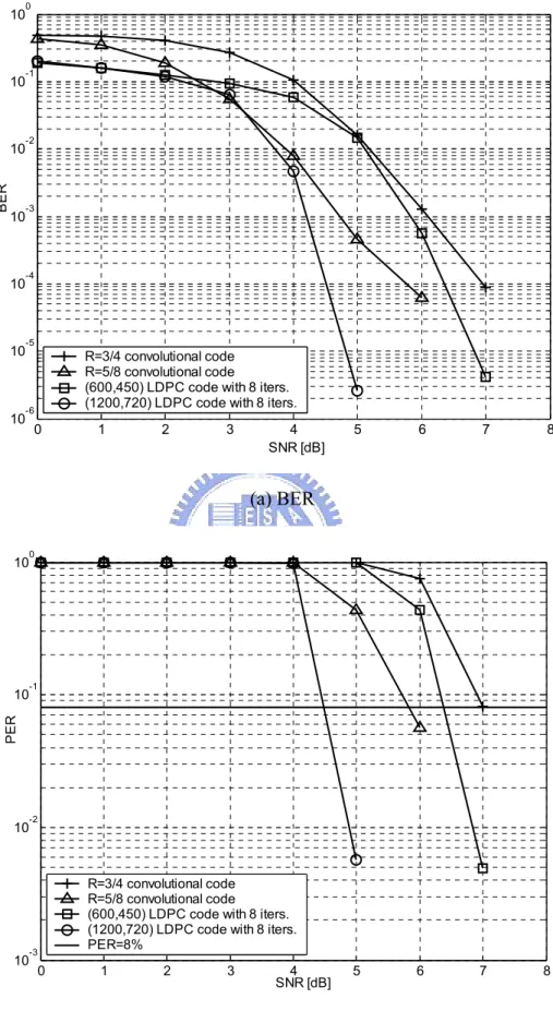
(41) 10. 10. BER. 10. 10. 10. 10. 10. 0. -1. -2. -3. -4. -5. R=3/4 convolutional code R=5/8 convolutional code (600,450) LDPC code with 8 iters. (1200,720) LDPC code with 8 iters.. -6. 0. 1. 2. 3. 4 SNR [dB]. 5. 6. 7. 8. 5. 6. 7. 8. (a) BER 10. -1. PER. 10. 0. 10. 10. -2. -3. 0. R=3/4 convolutional code R=5/8 convolutional code (600,450) LDPC code with 8 iters. (1200,720) LDPC code with 8 iters. PER=8%. 1. 2. 3. 4 SNR [dB]. (b) PER Fig. 3.8 Performance comparison for different codes 30.
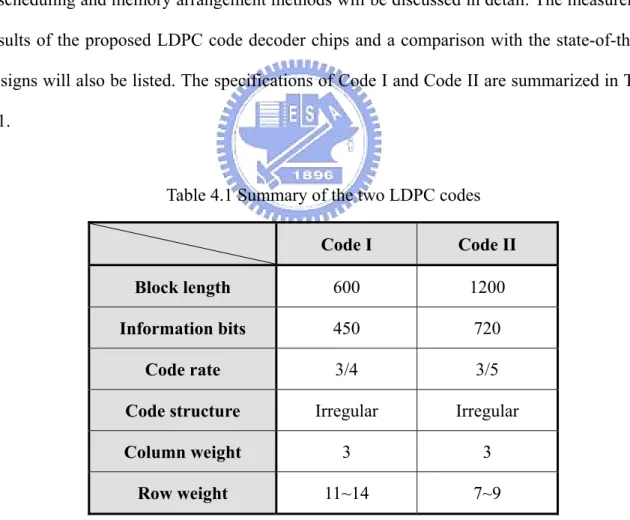
(42) Chapter 4 Architectures of Proposed LDPC Code Decoders The architectures of the proposed LDPC code decoders for two different LDPC codes, Code I and Code II, will be introduced in this chapter. Basic functional units, data flow rescheduling and memory arrangement methods will be discussed in detail. The measurement results of the proposed LDPC code decoder chips and a comparison with the state-of-the-art designs will also be listed. The specifications of Code I and Code II are summarized in Table 4.1.. Table 4.1 Summary of the two LDPC codes. Code I. Code II. Block length. 600. 1200. Information bits. 450. 720. Code rate. 3/4. 3/5. Code structure. Irregular. Irregular. Column weight. 3. 3. Row weight. 11~14. 7~9. 31.
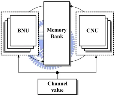
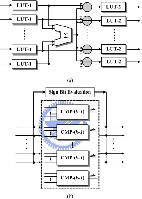
(43) 4.1. Introduction to the Conventional Design Based on the decoding algorithm, the block diagram of conventional LDPC code decoder. is shown as Fig. 4.1. The bit node unit (BNU) is dedicated to the vertical step, while the check node unit (CNU) is used for the horizontal step. The BNU (or CNU) reads and processes the messages stored in the memory bank, and write them back into the memory bank after updating. It can be noticed that a large number of combinational feedback paths exist between the CNU (or BNU) and the memory unit, leading to the complex signal routing as well as degradation of the decoding speed in the VLSI implementation.. BNU BNU BNU. Memory Bank. CNU CNU CNU. Channel value. Fig. 4.1 Block diagram of conventional LDPC code decoder. The conventional architecture of the CNU which is based on the LLR-SPA in (2.33) is shown in Fig. 4.2(a). The look-up tables (LUT) are used to implement the hyperbolic tangent (tanh) and inverse hyperbolic tangent (tanh-1) functions. The CNU can be implemented based on the min-sum algorithm as shown in Fig. 4.2(b) to reduce the hardware cost. As described in (2.38), the operations in the CNU can be divided into two parts: the sign evaluation and the minimum absolute value searching. The minimum 32.
(44) absolute values are searches by k comparators which consist of k-1 inputs (CMP-(k-1)), where k is the row weight of the parity check matrix. LUT-1. -. LUT-1. -. LUT-2 LUT-2. ∑ LUT-1. LUT-2. -. LUT-1. LUT-2. (a) Sign Bit Evaluation. CMP-(k-1). min. CMP-(k-1). min. CMP-(k-1). min. CMP-(k-1). min. (b) Fig. 4.2 Architecture of conventional CNU based on: (a) LLR-SPA and (b) min-sum algorithm. The conventional BNU architecture with k inputs is shown in Fig. 4.3, where the SUM-(k-1) is used to sum up k-1 values. Note that there is no difference on the BNU design between the LLR-SPA and the min-sum algorithm. Both LLR-SPA and min-sum algorithm have the same BNU design. 33.
(45) SUM(k-1). SUM(k-1). SUM(k-1). channel value. Fig. 4.3 Architecture of conventional BNU. 4.2. Proposed LDPC Code I Decoder Design The LDPC code decoders have inherently parallelism due to the non-dependency among. check node updates or bit node updates; the throughput can be improved by linear increase of the hardware costs. However, the full-parallel implementation [9] is non-area-efficient for a system chip design. Therefore the partial-parallel architecture is employed in the proposed decoders to reduce circuit complexity according to the system requirements. In time-division multiplexing mode, the partial-parallel LDPC code decoders map a certain number of check nodes or bit nodes into a single processing unit. Extra decoding latencies are produced as compared with the full-parallel implementations. Thus a trade-off is made between the decoding speed and the hardware complexity. Besides, to simplify the hardware cost, the min-sum algorithm is chosen to implement the proposed design while keeping the system performance.. 34.
(46) Fig. 4.4 presents the architecture of the proposed LDPC Code I decoder containing the distributor, memory unit, switch groups, CNU and BNU. Since the irregular parity check matrix H has a fixed number of column weight (= 3), the total number of weight in parity check matrix is 600 × 3 = 1800. To implement the decoder in a partial-parallel mode, the check nodes in the corresponding bipartite graph are partitioned into three parts, and the bit nodes are divided into four parts as shown in Fig. 4.5, where every three check nodes share a single CNU, and every four bit nodes share a single BNU. Therefore 150/3 = 50 CNUs and 600/4 = 150 BNUs are required in the proposed design. The switch groups in Fig. 4.4 are used to select which part of check nodes or bit nodes is under operation.. MU2 MU2 MU2 BNUi. 450 symbols. Distributor. 600 symbols. 1800 symbols. MU MU22 MU CNU2i. Memory (1800*6b) MU2 BNU 150. 450 symbols. 1800 symbols. 1800 symbols. Switch 1. Switch 2. 600 symbols. 150 symbols. Switch 3 600 symbols. Channel Value (600*5b) Fig. 4.4 The architecture of LDPC Code I decoder. 35. MU2 CNU 50.
(47) Parity check matrix H. CNU set c1 c2 c3. BNU set. b1. b2. b3. b4. Fig. 4.5 The partition for parity check matrix H of Code I. Due to the random-like connections in the bipartite graph, the signal routing problem causes serious difficulties in the decoder implementation. As shown in Fig. 4.1, the combinational feedback paths leads to the degradation of the decoding speed and the routing area overhead in the VLSI implementation. In the proposed design, the pipeline registers are inserted in CNUs and BNUs to cut off those feedback paths as illustrated in Fig. 4.6. Thus, shorter critical path delay that reduces routing congestion can be achieved with little increases in the hardware costs.. CNU-PATH 2. BNU-PATH 1. BNU. Flip Flop. Flip Flop. Memory Bank BNU-PATH 2. CNU. CNU-PATH 1. Fig. 4.6 Data path of proposed partial-parallel decoder. 4.2.1. Channel Value Interconnection. For the conventional design in Fig. 4.1, both the CNUs and BNUs have to be connected to the channel values, which lead to large number of signal connections. Thus data 36.
(48) rescheduling is proposed to solve this problem in Fig. 4.7.. Initialization. Vertical Step. Iterative Decoding. Horizontal Step. No. Vertical Step. Syndrome Check. Yes. Output Estimated Bits. Fig. 4.7 Proposed LDPC decoding flow. As shown in Fig. 4.7, one extra vertical step is employed to replace the initialization through the CNUs. Recall equation (2.34) LBi →C j (eij ) = L( xi ) +. ∑. C j′ ∈M ( i )\ C j. LC j′ → Bi (eij′ ) ,. (2.34). only summations among the channel value L(xi) and the messages LC→B(eij) are performed in the BNUs. If the messages LC→B(eij) are set to zero during initialization, the channel values are thus loaded into the memory through the BNUs, and fed to the CNUs for the first horizontal step. In this scheme, only BNUs have to be connected to the channel values as illustrated in Fig. 4.4, leading to less signal routing costs with some increases in decoding latencies. Fig. 4.8 gives the timing diagram of the proposed LDPC Code I decoder, where bi and ci correspond to the active BNU and CNU set in Fig. 4.5. The design takes nine cycles to complete a decoding iteration, including 4 cycles for horizontal steps with the CNUs and 5 cycles for vertical steps with BNUs. Additional five cycles are used to complete the channel value loading as described above. Thus total 9*8 + 5 = 77 cycles are required to finish the decoding process of a codeword with 8 iterations.. 37.
(49) BNUPATH1. BNUPATH2. Memory. CNUPATH1. CNUPATH2 idle. iteration #1. active. b2. b1. b3. b2. b1. b4. b3. b1~2. b4. b1~3. Time. channel value loading. b1. b1~4. c1. b1~4. c2. c1. c1. c3. c2. c1~2 b1. c3. c1~3. b2. b1. c1~3. b3. b2. b1. b4. b3. b1~2. b4. b1~3. Fig. 4.8 Timing diagram of the proposed LDPC Code I decoder. 4.2.2. Check Node Unit. As shown in Fig. 4.2(b), k comparators which search the minimal values among k-1 inputs are needed to implement the CNU based on the min-sum algorithm. As mentioned in [18], equation (2.38) can be modified as. 38.
(50) ( L (e ) ) ⎧ min L ( (e ) ) , if L (e ) ≠ min ( L ⎞ ⎪ (e )) ⎟⎟× ⎨ (e ) ) , otherwise ⎠ ⎪ 2 min ( L ⎩. ⎛ LCj →Bi (eij ) ≈ ⎜⎜ ∏ sign LBi′ →Cj (ei′j ) ⎝ Bi′∈L( j)\Bi. (. ⎛ = ⎜⎜ ∏ sign LBi′ →Cj ⎝ Bi′∈L( j)\Bi. (. ⎞. ) ⎟⎟ ⎠. min. Bi′ →Cj. Bi′∈L( j )\ Bi. Bi′ →Cj. Bi′∈L( j ). i′j. nd. Bi′∈L( j ). i′j. i′j. Bi′ →Cj. Bi →Cj. ij. Bi′∈L( j ). Bi′ →Cj. ). (ei′j ) , (4.1). i′j. where “2nd min” denotes the value which is smaller than all the other candidates except the minimal one. According to (4.1), the absolute value searching has to be performed only one time to find the minimum and the second minimum. Fig. 4.9 shows the block diagram of the compare-select unit (CS14) which searches for the minimal and the second minimal values from 14 inputs.. M1. M2. min. If (M1 == min) New M 1 = 2nd min; else New M 1 = min;. New M 1. If (M2 == min) New M 2 = 2nd min; else New M 2 = min;. New M 2. If (M14 == min) New M 14 = 2nd min; else New M 14 = min;. New M 14. CMP-14 2nd min M14. Selection Control Fig. 4.9 Block diagram of CS14. Because the column weight of Code I is ranging from 11 to 14, the CNUs dealing with different number of inputs should be designed. In this section, only the 14-input CNUs are introduced and others are designed in the analogous approach. The detailed architecture of CMP-14 in Fig. 4.9 is illustrated as Fig. 4.10, which consists of the pipeline registers and two 39.
(51) kinds of comparators: CMP-2 and CMP-4. CMP-4 finds out the minimal and the second minimal values from the four inputs, a, b, c, and d. In addition, CMP-2 is a two input comparator which is much simpler than CMP-4.. a b 5. a c 5. a d. 5. SUB. 5. 5. SUB. 1. 5. 5. SUB. 1. MSB5. b c 5. 5. c d 5. 5. 5. SUB. SUB. SUB. 1. 1. 1. MSB2. MSB1. MSB0. 1. MSB4. b d. MSB3. Decoder 2 nd min. min 5. 5. 2nd min. min. Fig. 4.10(a) Block diagram of proposed CMP-4 5. 5. 5. 5. CMP-4 min FF. nd. 2 min FF. 5. 5. 5. 5. 5. CMP-4 min. 2 min. min. FF. FF. CMP-4 min. 5. 5. CMP-4. nd. FF. 5. nd. 2 min FF. 5. 5. CMP-2 min. 2 nd min. FF. FF. CMP-4. nd. 2 min. min. CMP-2 min 5. min. 5 nd. 2 min. Fig. 4.10(b) Block diagram of proposed CMP-14. The proposed architecture of the 14-input CNU is shown in Fig. 4.11, where SM14 is sign-multiplication. To facilitate the operations on the sign and absolute value, all the 6-bit 40.
(52) values have been represented by the sign-magnitude notation with 2 integer bits and 4 fractional bits. The combinational path in the CNUs is cut off into CNU-PATH1 and CNU-PATH2 by the pipeline registers, leading to shorter critical path delay that reduces routing congestion.. CNU-PATH1. CNU-PATH 2 1(MSB) 6 5. 1(MSB) 5. FF. 1(MSB) 6 5. 6. .... .... FF. .... 6 1(MSB) 5. SM14. FF. 5. min FF. .... 1(MSB). CMP-14. 6. FF. FF. nd. Selection Control. 2 min. 1(MSB) 6 5. CS14 Fig. 4.11 The proposed 14-input CNU architecture. Table 4.2 lists the comparisons of three different CNU architectures. The LUT-1 and LUT-2 in Fig. 4.2(a) are implemented in 6-bit precision, including 2 integer bits and 4 fractional bits. The proposed CNU has the smallest size which is only about 22% of the others, whereas the maximum achievable operating speed is only a little smaller than conventional MS designs. Due to the fixed point implementation, some performance loss is produced. As a result, the decoder is implemented efficiently by using of the proposed CNU architecture.. 41.
(53) Table 4.2 Comparison of different CNU architectures. 4.2.3. LUT Fig. 4.2(a). Conv. MS Fig. 4.2(b). Proposed Fig. 4.11. Max. speed. 162 MHz. 261 MHz. 250 MHz. Gate count. 7.16 K. 6.86 K. 1.6 K. Total gate count. 358 K. 343 K. 80 K. Bit Node Unit. Fig 4.12 shows the block diagram of BNU. According to equation (2.34) and (2.35), the BNUs receive the channel value and the message values linked to the same bit node. All inputs with sign-magnitude (SM) notation are converted to be 2’s complement (TC) representation, and summed to perform the updating calculation. The pipeline registers are inserted to break the critical paths into BNU-PATH1 and BNU-PATH2 as in the CNUs. Finally, all the values are converted back to the SM notation and clipped to avoid overflow. And the most significant bit (MSB) of the summation of the three input messages and the channel value is used to decide the estimated codeword bit. All the 6-bit values are quantized with 2 integer bits and 4 fractional bits, while the intermediate summations are represented with 4 integer bits and 4 fractional bits.. 42.
(54) BNU-PATH1. C1. 6. C2. 6. SM→TC. SM→TC. 6. BNU-PATH2. +. 6. Channel value. 6. 5. SM→TC. SM→TC. FF. +. 8. 8. TC→SM. Clipping. TC→SM. Clipping. TC→SM. Clipping. 6. new C3. 6. new C1. 6. new C2. 8. 6. 5. FF. FF. + C3. 8. 8. FF. 8. 8. +. (MSB) 1 Decoded. bit. Fig. 4.12 The proposed BNU architecture. Note that if C1, C2 and C3 are set to be zero during initialization, the channel value will be directly bypassed to the outputs of BNU. This produces a path to load the channel values into the memory as mentioned above.. 4.2.4. Chip Implementation. The proposed LDPC Code I decoder was implemented within an LDPC-COFDM UWB baseband transceiver chip [25] with the 0.18 µm 1P6M standard CMOS process. The chip micrograph of the entire UWB transceiver including the OFDM modem and the LDPC codec is given in Fig. 4.13. The encoder die size is 2.25 mm2, while the decoder die size is 16.5 mm2. The total gate count of the LDPC codec is 542 K, where 70K is for the encoder and 472K is for the decoder. The chip has been tested to verify the functional correctness. The measured maximal data rate of the decoder is 480 Mb/s while working at 82.1 MHz, and consuming 232 mW. The detailed chip features are also summarized in Table 4.3.. 43.
(55) LDPC Encoder. OFDM Modem. LDPC Decoder. Fig. 4.13 Die micrograph of the LDPC-COFDM UWB transceiver chip. Table 4.3 Summary of the LDPC Code I Chip. Technology. Standard 0.18-µm CMOS 1P6M. Package. CQFP-208. Supply voltage. 1.8V core, 3.3 V I/O. Encoder. 1.5mm × 1.5mm. Decoder. 5.0mm × 3.5mm. Encoder. 70K. Decoder. 472K. Chip size. Gate count Power dissipation. 232mW @ 82.1MHz. Maximum data rate. 480Mb/s. 44.
(56) 4.3. Proposed LDPC Code II Decoder Design In Sec. 4.2, the proposed LDPC Code I decoder design is introduced and silicon proven. to achieve 480Mb/s maximum data rate. The performance of LDPC code I decoder is acceptable for the MB-OFDM UWB system [23], but may be not for other high-speed communication systems mentioned in Chap. 3. As a result, the LDPC code II decoder is proposed to get better error-correcting ability and higher decoding throughput. While considering circuit complexity, the 480 × 1200 parity check matrix H of LDPC code II are divided into four 240 × 600 sub-matrixes to fit partial-parallel architecture, which is shown in Fig. 4.14. Since matrix H of Code II has a fixed number of column weight (= 3), the total number of weight is 1200 × 3 = 3600. Based on this partition, the functional units in the decoder will process 1800 messages every cycle.. h00. h01. CNU Set 1. h10. h11. CNU Set 2. H=. BNU Set 1 BNU Set 2. Fig. 4.14 The partition of parity check matrix H of Code II. The proposed LDPC code II decoder architecture illustrated in Fig. 4.15 contains the input buffer, 240 CNUs, 600 BNUs and two dedicated message memory units (MMU). The set of data processed by CNUs are {h00, h01} and {h10, h11}, whereas the data fed into BNUs should be {h00, h10} and {h01, h11}. Note that two MMUs are employed to process two different codewords concurrently without stalls. Therefore, the LDPC decoder is not only area-efficient but the decoding speed is compatible with the fully parallel architecture. The detail ideas about the designs of MMUs will be introduced in the following. 45.
(57) The input buffer is a storage component that receives and keeps channel values for iterative decoding. Note that it only connects to the BNUs to get less routing congestion as discussed in Sec. 4.2.1.. Input Buffer buf-0. buf-1. MMU-1. B. buf-2. buf-3. A 1800 symbols. E. D. 600 BNUs. C. 1800 symbols. 1800 symbols. 240 CNUs. 600 symbols. C. D. A. B. E. 1800 symbols. MMU-0. Fig. 4.15 The proposed LDPC code II decoder architecture. 4.3.1. Input Buffer. Input buffer provides the channel values to the BNUs for iterative decoding. Because two different codewords are processed concurrently, total 1200 × 2 = 2400 symbols should be stored in the input buffer. According to the partition in Fig. 4.14, the buffer is divided into four sub-blocks, where each sub-block contains 600 channel values. The conventional design is illustrated in Fig. 4.16. Four sub-blocks, buf-0 ~ buf-3, are all connected to the channel 46.
(58) value inputs, and multiplexers are employed to switch appropriate values into the BNUs. Thus the signal routings are all “global”, meaning that all the connections are related to the inputs and outputs (I/O) of the buffer. The global connections and the multiplexers will lead to serious routing congestion. Channel value inputs. buf-0. buf-1. buf-2. buf-3. To BNU. Fig. 4.16 The conventional architecture of input buffer. Fig. 4.17 shows the buffer structure based on register exchange (RE) approach and the operational timing diagram, where buf-0 is designed as a shift register that serially receives the channel values from inputs and the other three sub-blocks exchange the data with buf-0 sequentially. The notation E1, E2 and E3 represent the data exchange from buf-0 to buf-1, buf-2 and buf-3, respectively. During initialization, buf-0 serially receives the channel values and passes them into other sub-blocks by executing the operations E1, E2 and E3 when buf-0 is full-filled.. buf-3. buf-2 E3. buf-1. E1. E2. buf-0. To BNU. Channel value inputs. Fig. 4.17(a) The architecture of RE based input buffer 47.
(59) Channel Value C00. C01. C10. iteration #1. initialization. Codeword 0. C11. Codeword 1. buf-0 C00. buf-1. C01. C00. C10. C00. C01. C11. C00. C01. C10. C00. C11. C01. C10. C01. C11. C00. C10. C10. C11. C00. C01. C11. C10. C00. C01. C00. C10. C11. C01. buf-2. buf-3. Data shift-in empty. Fig. 4.17(b) The timing diagram of RE based input buffer. For this RE based buffer architecture, the global interconnections exist only in buf-0, and all the others are “local” among sub-blocks. However, the drawback is that a large number of multiplexers are required around buf-0 to perform E1 ~ E3. Thus buf-0 becomes a routing-critical block due to the multiplexers and the global interconnections. To overcome this problem, an architecture based on register shifting (RS) is proposed as shown in Fig. 4.18(a), where four sub-blocks are arranged in a ring. The buf-0 is a shift register that serially receives the channel values and buf-3 transports the associated channel values to BNU. The timing diagram of the RS-based input buffer is presented in Fig. 4.18(b). Channel values of two different codewords are serially fed into buf-0, and shifted within the buffer ring when buf-0 is full-filled. Therefore, the data flow is further simplified, and the multiplexers are eliminated, leading to simple signal transfer and routing interconnections.. 48.
(60) buf-1. buf-0. Channel value inputs. buf-2. buf-3. To BNU. buf-0 C00. buf-1. initialization. C01. C00. C10. C01. C00. C11. C10. C01. C00. iteration #1. (a). C00. C11. C10. C01. C01. C00. C11. C10. C10. C01. C00. C11. C11. C10. C01. C00. buf-2. buf-3. Data shift-in empty. (b) Fig. 4.18 The architecture and timing diagram of RS-based input buffer. Fig. 4.19 gives the comparison of the three input buffer architecture. The RS-based input buffer can save about 20% gate count and 30% interconnection wires as compared with the conventional design.. 49.
(61) 4. 9. x 10. 83825. gate count number of interconnection. 81830. 8 7. 67855. 6 5 4 3. 30000 24000. 2. 21000. 1 0. Conventional. RE. RS. Fig. 4.19 The comparison of three input buffer designs. 4.3.2. Check Node Unit and Bit Node Unit. Fig. 4.20 shows the CNU architecture for proposed LDPC code II decoder. The CNU can be divided into two parts: one is 1-bit sign-multiplication (SM) and the other is 5-bit compare-and-select unit (CS) that searches the minimal value and the second minimal value from the inputs. The new message for each bit node is a combination of the sign bit according to (4.1) and the new magnitude which is either “min” or “2nd min” of the CS unit. The detailed architecture of CMP-9 in Fig. 4.20 is designed as that shown in Fig. 4.9 and 4.10. The BNU architecture is illustrated in Fig. 4.21. According to (2.34) and (2.35), BNU receives the channel value and the messages linked to the same bit node. All inputs with sign-magnitude (SM) notation are firstly converted to be 2’s complement (TC) representation, and then summed to perform the updated calculation. The summed values are also clipped to 50.
數據
+7
相關文件
Real Schur and Hessenberg-triangular forms The doubly shifted QZ algorithm.. Above algorithm is locally
In this chapter we develop the Lanczos method, a technique that is applicable to large sparse, symmetric eigenproblems.. The method involves tridiagonalizing the given
Using this formalism we derive an exact differential equation for the partition function of two-dimensional gravity as a function of the string coupling constant that governs the
Courtesy: Ned Wright’s Cosmology Page Burles, Nolette & Turner, 1999?. Total Mass Density
//Structural description of design example //See block diagram
Teacher then briefly explains the answers on Teachers’ Reference: Appendix 1 [Suggested Answers for Worksheet 1 (Understanding of Happy Life among Different Jewish Sects in
• Given a (singly) linked list of unknown length, design an algorithm to find the n-th node from the tail of the linked list. Your algorithm is allowed to traverse the linked
The schematic diagram of the Cassegrain optics is shown in Fig. The Cassegrain optics consists of a primary and a secondary mirror, which avoids the generation of
