適用於正交分頻多工系統之快速傅立葉轉換處理器設計
99
0
0
全文
(2) 適用於正交分頻多工系統之快速傅立葉轉換處理器設計 FFT Processor Design for OFDM Systems 研 究 生:陳坤隆. Student:Kun-Lung Chen. 指導教授:陳紹基 博士. Advisor:Sau-Gee Chen. 國 立 交 通 大 學 電子工程學系 電子研究所碩士班 碩 士 論 文. A Thesis Submitted to Department of Electronics Engineering & Institute of Electronics College of Electrical Engineering and Computer Science National Chiao Tung University in Partial Fulfillment of the Requirements for the Degree of Master of Science in Electronics Engineering June 2004 Hsinchu, Taiwan, Republic of China. 中華民國九十三年六月.
(3) 適用於正交分頻多工系統之快速傅立葉轉換處 理器設計 學生:陳坤隆. 指導教授:陳紹基 博士. 國立交通大學 電子工程學系 電子研究所碩士班. 摘. 要. 為了設計一個具低複雜度、低成本的可變長度快速傅立葉轉換處理器以適 用於多種正交分頻多工的通訊系統,本論文由演算法至架構層次研究各種關於 快速傅立葉轉換的技術。本論文並提出了改進的可變長度資料位址產生器、新 的轉動因子產生器以及應用新座標旋轉演算法的新快速傅立葉轉換處理單元。 其中可變長度資料位址產生器將原先耗費面積的桶形移位器設計簡化成應用多 工器的簡單定址函數設計;相較於現行的快速傅立葉轉換運算之轉動因子產生 器,新的轉動因子產生器擁有高速與低複雜度的優點;相較於已知的座標旋轉 設計,新的座標旋轉演算法與其快速傅立葉轉換處理單元設計擁有較少的重複 執行次數,而且應用座標旋轉演算法的快速傅立葉轉換處理單元不需要額外的 記憶體來儲存轉動因子。最後,本論文提出一個以座標旋轉演算法來設計處理 單元之可變長度快速傅立業轉換處理器的架構,並可適用於 802.16a、數位音訊 廣播、以及數位影像廣播等多種通信標準。. I.
(4) FFT Processor Design for OFDM Systems. Student: Kun-Lung Chen. Advisor: Dr. Sau-Gee Chen. Department of Electronics Engineering & Institute of Electronics National Chiao Tung University. ABSTRACT In order to design a low-complexity and low-cost variable-length FFT processor module suitable for various OFDM communication systems, the thesis first studies various design techniques from algorithm level to architecture level. Then the thesis proposes an improved variable-length data address generator, a new twiddle factor generator and a new CORDIC-based FFT PE based on a new CORDIC algorithm. The variable-length data address generator simplifies the original area-consuming barrel-shifter based designs with a few simpler multiplexer-based addressing functions. The twiddle factor generator has the merit of low complexity and high speed over the existing twiddle factor generators for practical FFT operations. A CORDIC-based FFT PE has the advantage that it does not need extra memory to store twiddle factors. The new CORDIC algorithm and its FFT PE design have lower iteration counts than the known CORDIC design. Finally, the thesis synthesizes a multi-standard variable-length CORDIC-based FFT processor, which is suited for 802.16a, DAB and DVB-T. II.
(5) 誌 謝 首先我要感謝指導教授 陳紹基博士兩年多來在課業上與研究上的悉心指導 與諄諄教誨,每當我在研究上產生疑惑時老師都能適時地指點迷津,使得本篇 論文之研究得以順利進行,在此致上由衷的感激與謝意。 再者,感謝曲老學長提供的協助與建議,讓我在理論及實作方面都有清楚正 確的概念,以及卓人學長在研究與生活上的意見與鼓勵。另外,感謝余承穎學 弟對於論文的協助與建議,以及 429 實驗室的夥伴們:明秀、育婷、a 貓、清泉、 觀易、世民、大條、元志、佳旻對我在課業及生活上的照顧、鼓勵與包容。 最後,對於我的父母親以及女友育卿長久以來的支持與鼓勵,謹致上無限的 敬意與感激。. III.
(6) Contents Chinese Abstract ....................................................................................................... I English Abstract ...................................................................................................... II Acknowledgement ..................................................................................................III Contents .................................................................................................................. IV List of Tables........................................................................................................... VI List of Figures........................................................................................................VII Chapter 1 Introduction.............................................................................................1 1.1 OFDM Background .....................................................................................1 1.2 Motivation and Goal ....................................................................................3 1.3 Organization of the Thesis ...........................................................................4 Chapter 2 Review of FFT Algorithms and Architectures......................................5 2.1 Introduction..................................................................................................5 2.2 Key FFT Algorithms ....................................................................................6 2.2.1 Radix-2 DIF FFT Algorithm...............................................................6 2.2.2 Radix-4/ Radix-22 DIF FFT Algorithm...............................................7 2.2.3 Radix-8/ Radix-23 DIF FFT Algorithm.............................................10 2.3 Classification of FFT Architectures ...........................................................13 2.3.1 Pipeline-Based FFT Architectures ....................................................13 2.3.2 Memory-Based FFT Architectures ...................................................16 Chapter 3 Data Address Generation and Twiddle Factor Generation ..............17 3.1 Data Address Generation ...........................................................................17 3.1.1 Fixed-length Data Address Generator...............................................18 3.1.2 Variable-length Data Address Generator...........................................21 3.1.3 The Proposed Variable-length Data Address Generator ...................29 3.1.4 Comparison .......................................................................................38 3.2 Twiddle Factor Generation.........................................................................39 3.2.1 ROM-based Twiddle Factor Generator.............................................40 3.2.2 The Proposed Recursive Twiddle Factor Generator .........................41 3.2.3 Comparison .......................................................................................45 Chapter 4 Processing Elements of FFT Processor ...............................................48 4.1 Multiplier-based Processing Element ........................................................48 4.2 CORDIC-based Processing Element .........................................................50 IV.
(7) 4.2.1 Review of CORDIC Algorithm and Implementation .......................51 4.2.2 New Angle Decomposition and Table Size Reduction Schemes ......54 4.2.3 New On-line Variable Scale Factor Compensation Scheme.............58 4.2.4 The Overall Operation Flow and Architecture..................................61 4.2.5 Simulations Results...........................................................................65 4.2.6 Comparison .......................................................................................69 4.2.7 Proposed CORDIC-based PE ...........................................................71 4.3 Comparison of FFT Processing Elements..................................................73 Chapter 5 EDA Realization of the New Multi-Standard CORDIC-Based FFT Processor ..........................................................74 5.1 Design Overview .......................................................................................74 5.2 Components of FFT Processor...................................................................75 5.2.1 The Data Memory .............................................................................75 5.2.2 The Processing Element....................................................................76 5.2.3 Controller ..........................................................................................77 5.3 Design of Data Interface ............................................................................79 Chapter 6 Conclusion .............................................................................................83 Bibliography ............................................................................................................85 Autobiography.........................................................................................................91. V.
(8) List of Tables Table 1.1 Table 3.1 Table 3.2 Table 3.3. Basic specifications of some OFDM based communication standards ....2 Data addresses needed for butterfly PE in direct processing order ........23 Data address pairs for butterfly PE in Cohen’s scheme..........................23 Computing flows of the stage and butterfly counters for 16, 8 and 4 points DIF FFT (a) 16 points (b) 8 points (c) 4 points............................32 Table 3.4 Control signals of the SIB MUX array ...................................................33 Table 3.5 Four different configurations linking the desired data to the proper data memory bank...................................................................................36 Table 3.6 Comparison of the variable-length data address generators ...................38 Table 3.7 Reconstruct the values of all regions by 1/8-period sine/cosine.............40 Table 3.8 Area and speed simulation results of the proposed twiddle factor generator, with word length B=16 bits....................................................46 Table 3.9 Performance comparison of twiddle factor generators, B=16 ................47 Table 4.1 Comparison of complexity and critical path of complex multipliers .....50 Table 4.2 Recoding table for the decomposition of residual rotation angle, r=4....57 Table 4.3 Angle table of tan-12-i value for the 12-bit accuracy ...............................57 Table 4.4 Error term of the on-line scale factor compensation algorithm ..............60 Table 4.5 Comparison of the two new CORDIC processors ..................................64 Table 4.6 Detailed simulation results with 8-bit, 12-bit and 16-bit output accuracy ..................................................................................................65 Table 4.7 Occurrence percentage of the dominant factor between Tr or Ts, 12-bit precision .......................................................................................67 Table 4.8 Simulation results of different residue angle word length (a) 8-bit input and output accuracy (b) 12-bit input and output accuracy ............68 Table 4.9 Area and speed comparison of the new and several notable CORDIC processors (n-bit accuracy) .....................................................................70 Table 4.10 Percentages of twiddle factors which are equal to odd multiples of 45˚ in using the adopted radix-22 algorithm and the radix-22/2 PE ........71 Table 4.11 Comparison of the multiplier-based PE and CORDIC-based PE ...........73 Table 5.1 Power consumption of SRAM at 0.18µm process..................................76 Table 5.2 The required operation counts and clock rate of the proposed CORDIC-based PE to various OFDM communication specifications (output precision is 12-bit)......................................................................82. VI.
(9) List of Figures Figure 1.1 Figure 1.2 Figure 1.3 Figure 2.1 Figure 2.2 Figure 2.3 Figure 2.4 Figure 2.5 Figure 2.6 Figure 2.7 Figure 2.8 Figure 3.1 Figure 3.2 Figure 3.3 Figure 3.4. Traditional bandwidth allocation of a frequency multiplexing system....2 Bandwidth allocation of OFDM ..............................................................2 General architecture of an OFDM transceiver system.............................2 The butterfly signal flow graph of radix-2 DIF FFT ...............................6 Radix-2 DIF FFT signal flow graph of a 16-point example ....................7 The basic butterfly processing block of the radix-4 DIF algorithm.........8 Butterfly signal flow graph of a raidx-22 DIF FFT algorithm.................9 16-point signal flow graph of the radix-22 DIF FFT...............................9 The butterfly signal flow graph of the radix-8 DIF FFT algorithm.......11 The butterfly signal flow graph of the radix-23 DIF FFT algorithm.....11 Projection mapping of radix-2 DIF FFT signal flow graph ...................14 Data address generator for radix-r N-point DIF FFT.............................19 Block diagram of the fixed-length data address generator ....................20 Block diagram of the fixed-length coefficient generator .......................21 Butterfly processing sequence for memory based DIF FFT processors...............................................................................................22 Figure 3.5 Chang’s variable-length DIF data address generator .............................24 Figure 3.6 Block diagram of the Hung’s variable-length data address generator (a) The shift-insert-bypass multiplexer and the control signals (b) Shift-insert-bypass MUX array architecture (c) Full block diagram of DIF FFT data address generator ........................................................26 Figure 3.7 Data path of the radix-22/2 butterfly processing element (a) The datapath configuration of “radix-22-mode” (b) The datapath configuration of “radix-2-mode” ...........................................................30 Figure 3.8 SFG of 16, 8 and 4-point DIF FFT’s......................................................31 Figure 3.9 Variable-length data address generator ..................................................34 Figure 3.10 Block diagram of memory bank index generator ..................................37 Figure 3.11 Block diagram of the variable-length coefficient index generator ........38 Figure 3.12 Wave symmetry of a sine and cosine value ...........................................40 Figure 3.13 Architecture of the proposed twiddle factor generator (a) Architecture of the proposed generator for real part (cosine) of a twiddle factor (b) Combined twiddle factor generator architecture for interleaving computation of real and imaginary parts......................44 Figure 4.1 Fig. 4.1 (a) Complex multiplier structure of equation (4.1) (b) Complex multiplier structure Type I of equation (4.2) (c) Complex VII.
(10) Figure 4.2 Figure 4.3 Figure 4.4 Figure 4.5 Figure 4.6. Figure 4.7 Figure 4.8 Figure 5.1. multiplier structure Type II of equation (4.2) ........................................49 Flow chart of the new on-line scale factor compensation CORDIC algorithm ................................................................................................62 Architectures of the CORDIC algorithm (a) The 1st new CORDIC processor (b) The 2nd new CORDIC processor ....................................64 Fixed-point simulation results of new CORDIC algorithm...................65 The total occurrence percentage versus iteration number, 12-bit precision.................................................................................................66 SNR performance vs. internal datapath word length of the new CORDIC processor (a) 8-bit output accuracy (b) 12-bit output accuracy .................................................................................................69 Implement of twiddle factor WN/8 (angle value of CORDIC is 45˚) .....72 Block diagram of the Proposed CORDIC-based FFT PE......................72 Block diagram of the proposed FFT processor......................................74. Figure 5.2 The CORDIC-based PE structure ..........................................................77 Figure 5.3 The flow chart of the butterfly operations with proposed CORDIC-based PE ................................................................................78 Figure 5.4 Timing diagram of CORDIC-based FFT processor...............................78 Figure 5.5 Data interface structures for FFT PE (a) The 1st data interface structure for FFT PE (b) The 2nd data interface structure for FFT PE (c) The 3rd data interface structure for FFT PE.....................................80. VIII.
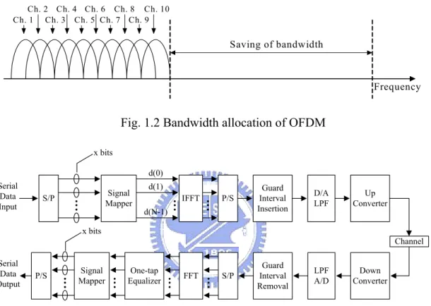
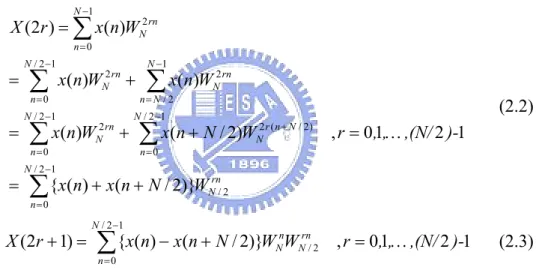
(11) Chapter 1 Introduction 1.1 OFDM Background In modern communication systems, the OFDM (Orthogonal Frequency Division Multiplexing) algorithm is effective in combating the problems of frequency-selective fading, inter-symbol interference (ISI), and inter-carrier interference (ICI). It is also efficient for wideband data transmission. Bandwidth allocation of traditional frequency multiplexing is shown in Fig. 1.1. The conventional systems not only keep all subchannels away from overlapping each other, but also allow some guard band bandwidth such that adjacent subchannels will not introduce inter-channel interference (ICI). This allocation method is inefficient in bandwidth utilization. OFDM, however, uses orthogonal carriers to modulate signal of subchannels and eliminate ICI that allow subbands overlap as shown in Fig. 1.2. Therefore, OFDM techniques play an important role in modern wireless and wireline communication systems, such as 820.11a/g, 802.16, DVB-T, DAB and so on. General architecture of OFDM system is shown in Fig. 1.3. The specifications of some OFDM-based communication standard are shown in Table 1.1.. 1.
(12) Ch.1. Ch.2. Ch.3. Ch.4. Ch.5. Ch.6. Ch.7. Ch.8. Ch.9. Ch.10. Frequency. Fig. 1.1 Traditional bandwidth allocation of a frequency multiplexing system Ch. 2 Ch. 4 Ch. 6 Ch. 8 Ch. 10 Ch. 1 Ch. 3 Ch. 5 Ch. 7 Ch. 9. Saving of bandwidth. Frequency. Fig. 1.2 Bandwidth allocation of OFDM x bits d(0). Serial Data Input. Signal Mapper. S/P. d(1). IFFT. P/S. d(N-1). Guard Interval Insertion. D/A LPF. Up Converter. x bits. Channel Serial Data Output. P/S. Signal Mapper. One-tap Equalizer. FFT. S/P. Guard Interval Removal. LPF A/D. Down Converter. Fig. 1.3 General architecture of an OFDM transceiver system. Table 1.1 Basic specifications of some OFDM based communication standards Standards. FFT size (duration per symbol). 802.11a. 64 (3.2µs). DAB DVB-T 802.16. Mode 1. Mode 2. Mode 3. Mode 4. 2048 (1ms). 512 (250µs). 256 (125µs). 1024 (500µs). 8K Mode. 2K Mode. 8192 (896µs). 2048 (224µs) 2048 (102.4µs). 2.
(13) 1.2 Motivation and Goal DFT/IDFT (realized by FFT/IFFT) is the core component in OFDM communication systems. Since architectures of different communication systems based on OFDM are very similar, integrating those receivers as a single hardware is worthy of investigation. The key integration work is to design a single FFT processor which adapts to various FFT lengths for different OFDM communication standards, including DAB, DVB-T and 802.16. Therefore, an efficient variable-length data address generator is required. The variable-length FFT processor should have little extra hardware cost compared with the fixed-length FFT processor. Furthermore, the required FFT lengths of those systems range from 256 to 8192. The required twiddle factors in FFT are generally stored in a look-up table in advance and retrieved for butterfly multiplication whenever necessary. This normally leads to a large ROM table, particularly for large FFT lengths such as 8192. Therefore, an efficient twiddle factor generator with small area and high speed performance is indispensable. Moreover, the conventional multiplier-based butterfly PE’s not only have high computing complexity but also require a twiddle factor generator either in the form of table or a function generator. In order to achieve low complexity and eliminate twiddle factor generator, CORDIC algorithm are investigated and applied to the design of an FFT PE.. 3.
(14) 1.3 Organization of the Thesis In Chapter 2, we review fundamental theory, including some key FFT algorithms based on Cooley-Tukey decomposition and popular FFT architectures. Chapter 3 discusses the address generation of memory-based FFT processors for both fixed-length and variable-length FFT. Designs of data address generator, coefficient index generator and processing element adapted to variable-length FFT applications will be proposed and explained in this chapter. Moreover, a new twiddle factor generator which has smaller area and lower complexity will be detailed as well. In chapter 4, a new CORDIC algorithm which combines a new on-line scale factor compensation method with a new rotation angle recoding scheme is proposed and considered as the key contribution of this thesis. Architecture of an CORDIC-based FFT PE based on the new CORDIC algorithm is also presented in this chapter. Finally, we synthesize a memory-based variable-length FFT processor with the proposed CORDIC-based PE in Chapter 5. In the end of this thesis, brief conclusions and ideas on future works will be presented in chapter 6.. 4.
(15) Chapter 2 Review of FFT Algorithms and Architectures 2.1 Introduction Discrete Fourier Transform (DFT) is widely applied to communications and digital signal processing. However, the computational complexities of direct implementations of DFT algorithms are too high to meet high-performance and low-cost design goal. Therefore, a fast DFT algorithm is indispensable. Since the early paper proposed by Cooley and Tukey in 1965 [1], numerous improvement have been done on the FFT algorithm. The Cooley-Tukey based FFT algorithms reduce the computational complexity from O(N2) to O(NlogN). Generally, those types of FFT algorithms can be defined as radix-2n FFT algorithms, which provide flexible implementation. There are two basic classes of FFT algorithms. One is the decimation-in-time (DIT) decomposition which rearranges DFT equation by decimating and regrouping time signals. Another is the decimation-in-frequency (DIF) decomposition which rearranges DFT equation by decimating and regrouping frequency signals. Both DIF and DIT algorithms utilize the symmetry and the periodicity of the complex sine wave WNkn = e-j(2π/N)kn combined with the idea of divide-and-conquer to reduce the DFT multiplicative computation. Since both DIF and DIT algorithms have the same computational complexity and signal flow, we only focus on DIF FFT algorithms.. 5.
(16) 2.2 Key FFT Algorithms The basic N-point DFT of a sequence x(n) is defined as: N −1. X (k ) = ∑ x(n)WNnk , k = 0,1,…… ,N-1, where WNkn = e − j ( 2π / N ) kn. (2.1). n=0. 2.2.1 Radix-2 DIF FFT Algorithm Radix-2 DIF FFT algorithm is developed by partitioning the frequency samples into even part and odd part. By dividing the DFT outputs into even-indexed and odd-indexed parts and utilizing the symmetry of twiddle factor, the even and odd frequency samples can be expressed as N −1. X (2r ) = ∑ x(n)WN2 rn n=0. =. N / 2 −1. ∑ n=0. =. x(n)WN2 rn +. N / 2 −1. ∑ x(n)W n=0. =. 2 rn N. +. N / 2 −1. N −1. ∑ x(n)W. 2 rn N. n= N / 2. N / 2 −1. (2.2). ∑ x(n + N / 2)W. 2 r ( n + N / 2) N. n=0. , r = 0 ,1,… ,(N/ 2 )-1. ∑{x(n) + x(n + N / 2)}W. rn N /2. n=0. X (2r + 1) =. N / 2 −1. ∑{x(n) − x(n + N / 2)}W W n N. n=0. rn N /2. , r = 0,1,… ,(N/ 2 )-1. (2.3). As shown, equations (2.2) and (2.3) are composed by two (N/2)-point DFTs. It is well known that one can combine these two equations as one basic butterfly (BF) module as shown in Fig. 2.1, where x(n) and x(n+N/2) are the input data.. x(n). +. x(n + N / 2). -. x(n) + x(n + N / 2). x. {x(n) − x(n + N / 2)}WNn. WNn. Fig. 2.1 The butterfly signal flow graph of radix-2 DIF FFT. 6.
(17) By recursive decompositions, we can further partition these two small DFTs into even smaller DFTs, and so on. Finally, the completed N-point radix-2 DIF FFT algorithm can be obtained. The example of a 16-point radix-2 DIF FFT, in signal flow graph, is shown in Fig. 2.2. x[0]. X[0]. x[1]. W40. x[2]. W41. x[3]. W80. x[4] x[5] x[6]. W82. W40. W83. W41. W160. x[8] x[9]. W161. x[10]. W162. W40 W41. x[11] x[12]. W164. W80. W165. W81. 6 16. 2 8. x[14] x[15]. X[12]. X[10] X[6] X[14] X[1]. W163. x[13]. X[4]. X[2]. W81. x[7]. X[8]. X[9] X[5] X[13] X[3]. W. W. W40. W167. W83. W41. X[11] X[7] X[15]. Fig. 2.2 Radix-2 DIF FFT signal flow graph of a 16-point example. We can find that order of the output frequency coefficients is bit-reversed, as shown in Fig. 2.2.. 2.2.2 Radix-4/ Radix-22 DIF FFT Algorithm Similar to radix-2 algorithm, the frequency-domain data indices of a DFT can be divided into four groups 4r, 4r+1, 4r+2, and 4r+3. Then equation (2.1) can be rewritten in terms of four partial sums as shown in equation (2.4). The corresponding basic butterfly processing block is shown in Fig. 2.3.. 7.
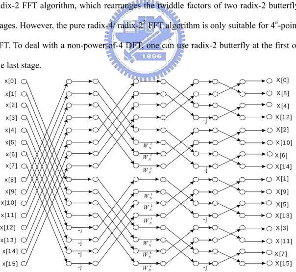
(18) X ( 4r + l ) =. N / 4 −1. N ) × W4l + 4 n=0 (2.4) 3N N 2l 3l nl nr x(n + ) × W4 + x(n + ) × W4 }WN WN / 4 ,where l = 0,1,2,3 2 4. ∑ { x ( n) + x ( n +. x(n) x(n+ N /4) x(n+ N /2). a(n). X. 4-point D FT. x(n+ 3N /4). X X X. 0n WN. 1n WN. 2n WN. a(n+ N /4) a(n+ N /2) a(n+ 3N /4). 3n WN. Fig. 2.3 The basic butterfly processing block of the radix-4 DIF algorithm. The relationship between inputs and outputs of the Fig. 2.3 are N N 3N ) + x(n + ) + x(n + ) 4 2 4 N N 3N a(n + N / 4) = {x(n) − x(n + ) × j − x(n + ) + x(n + ) × j}WNn 4 2 4 N N 3N a(n + N / 2) = {x(n) − x(n + ) + x(n + ) − x(n + )}WN2 n 4 2 4 N N 3N a(n + 3 N / 4) = {x(n) + x(n + ) × j − x(n + ) − x(n + ) × j}WN3n 4 2 4. a ( n ) = x ( n) + x ( n +. (2.5). Furthermore, if we substitute l for 2l1+l2, where l2 and l1 are equal to either 0 or 1, equation (2.4) can be rewritten as (2.6). Equation (2.6) is called radix-22 FFT algorithm and its butterfly signal flow graph is shown in Fig. 2.4. The complete signal flow graph of a 16-point radix-22 DIF FFT is shown in Fig. 2.5.. X (4r + 2l1 + l2 ) =. N −1 4. ∑{x(n) + (−1). l1. x( n +. n=0. + (−1)l 2 x(n +. N l2 )W4 4. N 3 N 3l 2 n ( 4 r + 2l1 + l 2 ) ) + (−1)l1 x(n + )W4 }WN 2 4. 8. (2.6).
(19) a(n). x[n]. +. +. x[n+N/4]. +. -. X. +. WN X. a(n+N/4). 2n. x[n+N/2]. -. a(n+N/2). 1n. WN x[n+3N/4]. -. -. X. a(n+3N/4). X 3n. -j. WN. Fig. 2.4 Butterfly signal flow graph of a raidx-22 DIF FFT algorithm The output data order of radix-4 approach is digit-reversed, while that of radix-22 approach is bit-reversed order (the same as radix-2 algorithm mentioned in previous section). In fact, the radix-22 FFT algorithm can be regarded as a modification of the radix-2 FFT algorithm, which rearranges the twiddle factors of two radix-2 butterfly stages. However, the pure radix-4/ radix-22 FFT algorithm is only suitable for 4n-point FFT. To deal with a non-power-of-4 DFT, one can use radix-2 butterfly at the first or the last stage. x [0 ]. X [0 ]. x [1 ]. X [8 ]. x [2 ]. X [4 ]. x [3 ]. -j. X [1 2 ] X [2 ]. x [4 ] x [5 ]. W N2. X [1 0 ]. x [6 ]. W N4. X [6 ]. x [7 ]. W N6. -j. X [1 ]. x [8 ] x [9 ] x [1 0 ] x [1 1 ]. W N1. X [9 ]. W N2. X [5 ]. W N3. x [1 2 ]. -j. x [1 3 ]. -j. W N3. -j. W. 6 N. -j. W N9. x [1 4 ] x [1 5 ]. X [1 4 ]. -j. X [1 3 ] X [3 ] X [1 1 ] X [7 ]. -j. Fig. 2.5 16-point signal flow graph of the radix-22 DIF FFT 9. X [1 5 ].
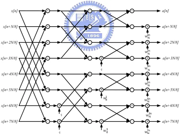
(20) 2.2.3 Radix-8/ Radix-23 DIF FFT Algorithm For the radix-8 DIF FFT algorithm, the index k of equation (2.1) is divided into eight subsets indexed by 8r+l, where l is from 0 to 7. With the properties of twiddle factor, equation (2.1) can be rewritten as the equation (2.7). The basic transformation unit is an 8-point DFT as shown in Fig. 2.6. N / 8 −1. 2N l 4 N 2l )W4 + x(n + )W4 8 8 n=0 6 N −l N 3N l + x(n + )W4 ] + [ x(n + ) + x(n + )W4 8 8 8 5 N 2l 7 N − l l nl rn + x(n + )W4 + x(n + )W4 ]W8 }WN WN / 8 8 8. X (8r + l ) =. ∑ {[ x(n) + x(n +. (2.7). Like radix-4 FFT algorithm, we can derive a radix-23 FFT algorithm from the radix-8 FFT algorithm by replacing index 8r+l with 8r+4l3+2l2+l1, as shown in equation (2.8). The basic butterfly blocks of radix-23 DIF FFT algorithm is shown in Fig. 2.7. X (8r + 4l3 + 2l2 + l1 ) =. N / 8 −1. 4 N l1 2N )W2 } + {x(n + ) 8 8 (2.8) 6 N l1 l 2 l1 5 N l1 N )W2 }W2 W 4} + {{x(n + ) + x(n + )W2 } + x(n + 8 8 8 3N 7 N l1 l 2 l1 4l3 + 2l 2 + l1 n ( 4l3 + 2l 2 + l1 ) nr ) + x(n + + {x( n + )W2 }W2 W4 }W8 }WN WN / 8 8 8. ∑ {{{x(n) + x(n + n=0. 10.
(21) x (n ). a (n ). X. x (n + N /8 ). 0 n. W. N. W. N. W. N. W. N. a (n + N /8 ). X. x (n + 2 N /8 ). 1 n. a (n + 2 N /8 ). X. x (n + 3 N /8 ). a (n + 3 N /8 ). X. 8 -p o in t DFT. x (n + 4 N /8 ). 2 n. 3 n. a (n + 4 N /8 ). X. x (n + 5 N /8 ). 4 n. W. N. W. N. W. 6 n N. W. 7 n N. a (n + 5 N /8 ). X. x (n + 6 N /8 ). 5 n. a (n + 6 N /8 ). X. x (n + 7 N /8 ). a (n + 7 N /8 ). X. Fig. 2.6 The butterfly signal flow graph of the radix-8 DIF FFT algorithm. x[n]. +. +. +. x[n+N/8]. +. +. -. a[n]. X. a[n+N/8]. 4n WN. x[n+2N/8]. +. +. -. X. a[n+2N/8]. 2n W N. x[n+3N/8]. -. +. X. -. X. a[n+3N/8]. +. 6n W N X. a[n+4N/8]. -j. x[n+4N/8]. -. +. 1n W N. x[n+5N/8]. -. +. X. -. 1 W8. x[n+6N/8]. -. X. -. X. X. a[n+6N/8]. 3n WN. -j. x[n+7N/8]. a[n+5N/8]. W5n N +. -. X. -. X. -. 3 W8. -j. X. a[n+7N/8]. 7n WN. Fig. 2.7 The butterfly signal flow graph of the radix-23 DIF FFT algorithm. 11.
(22) The relationship between inputs and outputs of Fig. 2.6 is 7. a ( n) = ∑ x ( n + m=0. 7 mN mN m n ), a (n + N / 8) = ∑{x(n + )W8 }WN 8 8 m=0. 7. a (n + 2 N / 8) = ∑{x(n + m=0 7. a (n + 4 N / 8) = ∑{x(n + m=0 7. a (n + 6 N / 8) = ∑{x(n + m=0. 7 mN 2 m 2 n mN 3m 3n )W8 }WN , a (n + 3 N / 8) = ∑{x(n + )W8 }WN 8 8 m=0 7 mN 4 m 4 n mN 5 m 5 n )W8 }WN , a (n + 5 N / 8) = ∑{x(n + )W8 }WN 8 8 m=0 7 mN 6 m 6 n mN 7 m 7 n )W8 }WN , a (n + 7 N / 8) = ∑{x(n + )W8 }WN 8 8 m =0. For Fig. 2.7, it is 7. a ( n) = ∑ x ( n + m=0. 7 mN mN 4 m 4 n ), a(n + N / 7) = ∑{x(n + )W8 }WN 8 8 m =0. 7. a (n + 2 N / 8) = ∑{x(n + m=0 7. a (n + 4 N / 8) = ∑{x(n + m=0 7. a (n + 6 N / 8) = ∑{x(n + m=0. 7 mN 2 m 2 n mN 6 m 6 n )W8 }WN , a (n + 3 N / 8) = ∑{x(n + )W8 }WN 8 8 m=0 7 mN m n mN 5 m 5 n )W8 }WN , a(n + 5 N / 8) = ∑{x(n + )W8 }WN 8 8 m=0 7 mN 3m 3n mN 7 m 7 n )W8 }WN , a (n + 7 N / 8) = ∑{x(n + )W8 }WN 8 8 m=0. Similar to radix-4/radix-22 case, output data ordering of radix-8 case is digit-reversed (where each digit contains three bits), while radix-23 case is bit-reversed.. 12.
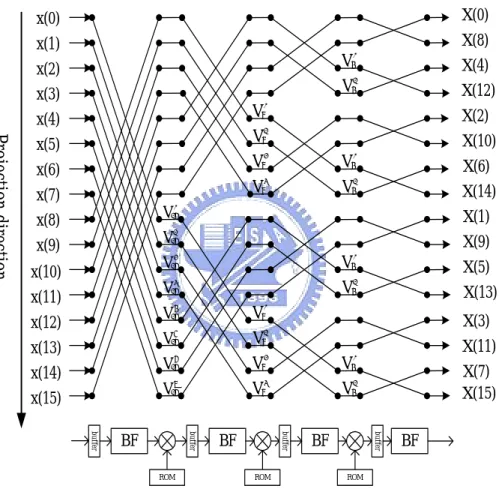
(23) 2.3 Classification of FFT Architectures Generally, FFT architectures can be classified as two categories: one is the pipeline-based architectures [2], [3], [4], [5], and the other is the memory-based architectures [6], [7], [8], [9], [10], [11]. These two types of architectures have their own advantages, disadvantages, and application purposes. The pipeline-based architecture is usually used in high throughput applications, because of high computation pipe stage. On the other hand, the memory-based architectures generally include a single butterfly PE (or more than one to enhance computation power), a centralized memory block to store input, output or intermediate data, and a control unit to handle memory accesses and data flow direction. Therefore, the hardware cost of a memory-based architecture is cheaper than pipeline-based architectures, but the negative side effect is a loss of throughput rate. We will introduce these two categories of FFT architectures in the following subsections.. 2.3.1 Pipeline-Based FFT Architectures Pipeline-based architectures are designed by emphasizing speed performance and the regularity of data path. The best way to obtain a pipeline-based FFT architecture is through vertical projection of signal flow graph (SFG) of designer’s algorithm selection. Fig. 2.8 shows a 16-point radix-2 DIF FFT example of projection mapping. The pipelined structure contains four butterfly processing elements (PE) (denotes as “BF” in Fig. 2.8) for addition and subtraction between two input data of each stage, three complex multiplier with coefficient look-up table, and four blocks of buffers to. 13.
(24) store and reorder data and provide smooth data flow for butterfly PE of the next stage. There are two types of data buffering strategies [5], [12], [13], [14] for pipeline based FFT processor. One is delay-commutator (DC) and the other is delay-feedback (DF). Multi-path structure is generally applied with delay-commutator type, and single-path structure is generally applied to delay-feedback type, which is called multi-path delay-commutator (MDC) and single-path delay-feedback (SDF), respectively. X(0). x(0). X(8). x(1). W40. x(2) x(3). X(4) X(12). W41 W80. x(4). X(2). Projection direction. W81. x(5) x(6) x(7). X(10). W82. W40. X(6). W83. W41. X(14). W160. x(8). X(1) X(9). W161. x(9) x(10) x(11) x(12) x(13) x(14) x(15). W162. W40. X(5). W163. W41. X(13). W164. W80. W165. W81. W166. W82. W40. W167. W83. W41. BF ROM. ROM. X(11) X(7) X(15) buffer. buffer. buffer. buffer. BF. X(3). BF. BF. ROM. Fig 2.8 Projection mapping of radix-2 DIF FFT signal flow graph. The SDF pipeline architecture is adaptable to various FFT algorithms such as radix-2, radix-4, radix-22, and higher-radix algorithms with (N-1) registers. The final output data order obtained from the SDF structure is always bit-reversed, and the utilization rate of the registers is 100%. Although FFT processor based an SDF architecture provides high performance throughput with simple control method, it suffers 14.
(25) from some disadvantages. For instance, the utilization rate of processing element isn’t 100%. The number of required arithmetic units depends on the number of pipeline stages. Furthermore, we need extra buffer to reorder output data because of the bit-reversed output order. MDC is also a flexible architecture that is adaptable to various FFT algorithms. Unlike SDF architecture, intermediate data are direct output to the next stage or coefficient multiplier instead of being written back, in a multi-path delay commutator (MDC) architecture. However, the MDC architecture also suffers from the similar disadvantages to the SDF architecture. The SDF has less hardware complexity and higher utilization rate, but longer FFT computation time, compared with MDC structures, assuming the same operating clock rate. The total time delay to compute an N-point FFT is expressed in equations (2.9), where TFFT is the clock cycle time operated on the radix-r algorithm and N is the length of FFT. SDF : TFFT = Tclk × N N MDC : TFFT = Tclk × r. (2.9). From these equations, one has the following conclusions: 1.. The computation time of an N-point FFT using the SDF pipeline architecture is independent of r. Therefore, a higher-radix algorithm does not imply a higher throughput rate, when realized by SDF structure.. 2.. The computation time of an N-point FFT in the MDC pipeline architecture will be reduced linearly with r. But it consumes large hardware estate with lower utilization rate when a high-radix algorithm is used.. 15.
(26) 2.3.2 Memory-Based FFT Architectures A general memory-based FFT processor structure mainly consists of a Butterfly PE, a main memory, ROM for twiddle factor storage, and a controller. The Butterfly PE is responsible for the butterfly operations required by FFT operations. Moreover, the architecture design of PE is dependent on the FFT algorithm used and generally dominates the performance of whole processor. The main memory stores processed data. The controller contains three functional units: data memory address generator, coefficient index generator, and operation state controller. The data memory address generator follows a regular pattern to generate several addresses, and then the main memory provides input data for butterfly PE and stores output data from butterfly PE according to these addresses. The coefficient index generator provides indices to select coefficients from coefficient ROM or maps to coefficients through twiddle factor generator. The data memory address generator and twiddle factor generator of memory-based FFT processor will be discussed in Chapter 3. Furthermore, the architecture designs of multiplier-based PE and CORDIC-based PE will be investigated in Chapter 4.. 16.
(27) Chapter 3 Data Address Generation and Twiddle Factor Generation 3.1 Data Address Generation Memory-based FFT processor architectures are designed to increase the utilization rate of butterfly PE’s. Different from the pipeline-based architectures, memory-based FFT processor often has one or two large memory block(s) that is accessed by all other PE components, instead of being distributed to many pipelined local arithmetic units. Main memory allocation and access strategy of a memory-based FFT processor can be classified as two types: in-place type [6], [7], [8], [9] and out-of-place type [10], [11], [15], [16], [17]. In in-place architecture, output data of butterfly PE are written back to the original memory bank with the same addresses as the previously loaded of input data. Alternatively, if output data are written to another memory block without overwriting input data, this design is generally called out-of-place. Therefore, memory size of the out-of-place design generally will be twice that of the in-place design. In in-place memory-based FFT processor, the data address generator design is based on butterfly execution order, while coefficient address is also dependent on the FFT algorithms and butterfly processing order. A conventional processing order and control scheme was proposed early by Cohen (1976) [18]. The algorithm was then. 17.
(28) extended and generalized by Johnson [6], Lo [7], and Ma [8], [9].. 3.1.1 Fixed-length Data Address Generator In Cohen’s scheme [18], the data addresses needed for the i-th butterfly of the k-th radix-2 FFT stage can be described by equation (3.1), while the operator ROTATEn(X, m) circularly rotates X left by m bits out of n bits. n = log2 N ⎧ s = ROTATEn (2i, k ) N , i = 0~ − 1, k = 0~n − 1 ⎨ 2 ⎩t = ROTATEn (2i + 1, k ). (3.1). Since the original Cohen’s scheme was based on DIT FFT, we can modify it to match the general DIF FFT algorithm such as described by equation (3.2), while the operator ROTATEn(X, m) circularly rotates X right by m digits out of n digits. N − 1, k = 0 ~ n − 1 r = ROTATE n (i, k ). n = log r N , i = 0 ~ address 0. address 1 = ROTATE n (i + M address r −1 = ROTATE n (i +. 1 N,k) r. (3.2). r −1 N,k) r. To realize equation (3.1), Cohen proposes are efficient address generator architecture based on barrel shifters. Similarly, architecture for executing equation (3.2) is shown in Fig. 3.1, which is modified from the Cohen’s proposed design [18]. The main idea is putting digits 0, 1..., and r-1 to MSB of the content of butterfly counter, and then using barrel shifters to achieve the circular rotation. The circular shift amount is equal to the content of the stage counter.. 18.
(29) Fig. 3.1 Data address generator for radix-r N-point DIF FFT. The memory access bandwidth is a critical issue in memory-based FFT processor design. An N-point memory-based FFT processor based on radix-r algorithm needs (N/r)logrN PE operations to transform one N-point symbol. Further, each PE operation needs 2r memory accesses to read data from memory and write back to it, so that each N-point symbol requires 2NlogrN memory accesses. In order to handle this requirement, there are two solutions: 1. Use a higher-radix algorithm to reduce total memory accesses. 2. Increase memory access bandwidth by using multiple memory ports. However, it is expensive to do so. Further, the number of memory ports is not controlled by architecture designer but cell library provider and device vendor. In addition, ideally the in-place design should simultaneously delivering r memory data to the radix-r butterfly PE and writing back r output data of butterfly PE to the data memory. Therefore, the solution to increase memory access bandwidth is to partition memory into r banks, and than store the data properly in the memory banks for conflict-free memory access.. 19.
(30) There are several efforts on memory partition and addressing methods to achieve conflict-free memory access [18], [6], [7]. The conflict-free memory partition scheme [6] that translates sequential data address data_count into bank index and data index of each memory bank is described in equation (3.3).. n = ⎡log r N ⎤ Data _ count = [d n −1d n − 2 ......d 2 d1d 0 ]r n −1. Bank _ index = (∑ dt ) mod r. (3.3). t =0. Data _ index = [d n −1d n − 2 ......d 2 d1 ]r Similar result can also be found in Lo’s scheme derived by vertex coloring rule [7]. The original data address data_count can be generated according to the content of the butterfly counter and the stage counter of FFT processing. The data_index is the new address assigned to each memory bank. For radix-r butterfly PE, this allocation algorithm can access r data from r different banks simultaneously at proper addresses according to the original data addresses. The data address generator with conflict-free memory accesses is often implemented by the following hardware [6], [7] as shown in Fig. 3.2.. Fig. 3.2 Block diagram of the fixed-length data address generator. 20.
(31) The coefficient index can be also generated from butterfly counter and stage counter. Its implementation [18] is generally simpler than the data address generator. The hardware diagram is shown in Fig. 3.3.. Fig. 3.3 Block diagram of the fixed-length coefficient generator. 3.1.2 Variable-length Data Address Generator In order to meet specifications of multi-mode and multi-standard OFDM communication systems, an FFT processor must support length-independent computation and meet the worst-case hardware requirement. Consequently, the FFT processor design must contains an efficient processing element, a variable-length data address generator and a variable-length twiddle factor generator. However, we can find out that Cohen’s scheme is not suitable for a variable-length FFT when we analyze a sub-segment of signal flow graph for a shorter-length FFT [19]. To give an example, a 16-point radix-2 DIF FFT is demonstrated as shown in Fig. 3.4. In direct-order we can process butterflies from top to down and from left stage to right stage as marked by the numbers on the right-hand sides of butterfly ellipses. On the other hand, since the main idea of Cohen’s processing order is grouping butterflies associated with the same twiddle factor together to reduce signal switching frequency of the coefficient circuits. This results in decima21.
(32) tion in butterfly (DIB) order as marked by the numbers on the left-hand sides of butterfly ellipses in Fig. 3.4. In the example, the data addresses needed for butterfly PE in direct processing order and in Cohen’s processing order are listed in Table 3.1 and Table 3.2 respectively. In the tables, <s, t> denotes data address pair for both input and output data for radix-2 butterfly PE, and s and t are indices of one dimension memory array. Note that the address translation and mapping from one dimension index to multi-bank memory system are considered later.. 1st stage 8-point. 16-point. 3rd stage. 2nd stage. 4th stage. 4-point 1. 1. 1. 3. 2. 1. 1. 5. 3. 2. 2. 7. 4. 3. 3. 4. 4. 5. 5. 6. 6. 7. 7. 2. 5. 8. 8. 4. 6. 6. 7. 8. 8. 1. 1. 5. 2. 2. 3. 6. 4. 2. 2. 3. 3. 4. 4. 5 3. 5. 7. 6. 4. 7. 8. 8. 1. 5. 6. 6. 7. 7. 8. 8. Fig. 3.4 Butterfly processing sequence for memory based DIF FFT processors. 22.
(33) Table 3.1 Data addresses needed for butterfly PE in direct processing order BF 0. BF 1. BF 2. BF 3. BF 4. BF 5. BF 6. BF 7. Stage 0. <0, 8>. <1, 9>. <2, 10>. <3, 11>. <4, 12>. <5, 13>. <6, 14>. <7, 15>. Stage 1. <0, 4>. <1, 5>. <2, 6>. <3, 7>. <8, 12>. <9, 13>. <10, 14>. <11, 15>. Stage 2. <0, 2>. <1, 3>. <4, 6>. <5, 7>. <8, 10>. <9, 11>. <12, 14> <13, 15>. Stage 3. <0, 1>. <2, 3>. <4, 5>. <6, 7>. <8, 9>. <10, 11> <12, 13> <14, 15>. Table 3.2 Data address pairs for butterfly PE in Cohen’s scheme BF 0. BF 1. BF 2. BF 3. BF 4. BF 5. BF 6. BF 7. Stage 0. <0, 8>. <1, 9>. <2, 10>. <3, 11>. <4, 12>. <5, 13>. <6, 14>. <7, 15>. Stage 1. <0, 4>. <8, 12>. <1, 5>. <9, 13>. <2, 6>. <10, 14>. <3, 7>. <11, 15>. Stage 2. <0, 2>. <4, 6>. <8, 10>. <12, 14>. <1, 3>. <5, 7>. <9, 11>. <13, 15>. Stage 3. <0, 1>. <2, 3>. <4, 5>. <6, 7>. <8, 9>. <10, 11> <12, 13> <14, 15>. In Fig 3.4, when we isolate the sub-SFG of a shorter-length FFT from the longer SFG, the Cohen’s DIB execution order mismatches with the variable-length FFT design concept. On the contrary, the direct processing order is suited for variable-length FFT operations. Therefore Cohen’s data address generation scheme has to be modified to deal with the operations of different FFT lengths. The direct ordered addressing scheme suitable for variable-length FFT design can be described by equation (3.4). In this equation, variable k and variable i are the contents of the stage counter and the butterfly counter, respectively, and the supported longest length of radix-r FFT is N.. 23.
(34) P = (r [(log r N ) − ( k +1)] ) address0 = (i − i mod P) × r + i mod P address1 = (i − i mod P) × r + P + i mod P M. (3.4). addressr − 2 = (i − i mod P) × r + (r − 2) P + i mod P addressr −1 = (i − i mod P) × r + (r − 1) P + i mod P Chang [19] proposed a variable-length data address generator, which was modified from Cohen’s fixed-length data address generator. In order to rotate the content of butterfly counter circular left first, the design includes an additional barrel shifter. The following operations that perform digit appending operations and rotate right circularly are similar to Fig. 3.1. The block diagram is shown in Fig. 3.5.. Fig. 3.5 Chang’s variable-length DIF data address generator. 24.
(35) When observing the results of equation (3.4) in digit representation, we can find that it is equivalent to dynamically inserting digit 0, 1…, r-1 into the middle position of the butterfly counter content. Equation (3.5) expresses the data address representation in digits, and the content of the stage counter denoted as variable k determines the insertion location of the butterfly counter content, which is indicated by variable i. For the data address, the right-side digits of the insertion location are equal to the content of the butterfly counter, while the left-side digits shifts the content of the butterfly counter by log2r bits. N ≡ digit number of the butterfly counter i r i = [ib −1 ib − 2 ib − 3 .....i2 i1 i0 ]r , k = 0 ~ b b = log r. address0 = [ib −1 ib − 2 ... ib − k 0 ib − k −1 ... i1 i0 ]r. (3.5). address1 = [ib −1 ib − 2 ... ib − k 1 ib − k −1 ... i1 i0 ]r M. addressr −1 = [ib −1 ib − 2 ... ib − k (r - 1) ib − k −1 ... i1 i0 ]r Based on the described property described above, we can use multiplexer arrays to perform the required shift and insertion operations instead of using barrel shifters. Hung [20] proposed a variable-length data address generator by simplifying the original area-consuming barrel-shifter based designs with simpler multiplexer-based addressing functions. In order to suit for 802.16a, DAB and DVB-T, the design covers seven different FFT lengths including 256, 512, 1024, 2048 and 8192 points. Furthermore, it is based on radix-22 DIF FFT algorithm but can still compute a general power-of-2 FFT by adding some minor modification to the original radix-22 architecture. The detailed block diagram is shown in Fig. 3.6.. 25.
(36) (a) The shift-insert-bypass multiplexer and the control signals. (b) Shift-insert-bypass MUX array architecture. (c) Full block diagram of DIF FFT data address generator Fig. 3.6 Block diagram of the Hung’s variable-length data address generator. 26.
(37) In Hung’s design as shown in Fig. 3.6, the stage counter and butterfly counter are designed to process the longest N-point FFT. When computing a shorter-length FFT such as N/2c, the butterfly counter simply adjust the count step from 1 to 2c instead of change the counting limit of the butterfly counter from N/2 to N/2c+1. This method result in scattered memory addresses. For example, the accessed memory locations of a 1024-point FFT are 0, 8, 16… and 8184 of the 8192-entry memory block. In order to access the data memory with continuous location, an additional shifter has to be used to convert the scattered data addresses to continuous values. Besides the design requirement of the butterfly counter, in order to support radix-2 and radix-22 modes, the stage counter is designed to have two different modes to match the butterfly counter operations and the multiplexer-based addressing functions. In non-power-of-4 FFT operations, the first stage must perform radix-2 computation, so that the radix-22 butterfly should be reconfigured as two radix-2 butterflies and the data addresses <s, t, u, v> required by butterfly PE are generated by the following equation (3.6). s = [00i(log 2 N ) −1i(log 2 N ) − 2 ... i2 i1 i0 ]2 t = [01i(log 2 N ) −1 i(log 2 N ) − 2 ... i2 i1 i0 ]2 u = [10i(log 2 N ) −1 i(log 2 N ) − 2 ... i2 i1 i0 ]2. (3.6). v = [11i(log 2 N ) −1 i(log 2 N ) − 2 ... i2 i1 i0 ]2 In addition, the data addresses <s, t, u, v> are described in equation (3.7) when processing varying stages of a power-of-4 point FFT expect the first stage. s = [i(log2 N ) −1 i(log2 N ) −2 ... i(log2 N ) − K 00i(log2 N ) − K −1 ... i1 i0 ]2 t = [i(log2 N ) −1 i(log2 N ) −2 ... i(log2 N ) − K 01 i(log2 N ) − K −1 ... i1 i0 ]2 u = [i(log2 N ) −1 i(log2 N ) −2 ... i(log2 N ) − K 10i(log2 N ) − K −1 ... i1 i0 ]2 v = [i(log2 N ) −1 i(log2 N ) −2 ... i(log2 N ) − K 11 i(log2 N ) − K −1 ... i1 i0 ]2. 27. (3.7).
(38) Hence, a special designed stage counter, which is denoted as K, is increased by one each time when performing a radix-2 butterfly operations or increased by two each time after all the radix-22 butterfly operations of an FFT stage are completed. For example, the sequences of the stage counter for a power-of-4 operation are 0, 2, 4 …, 2a, while the sequences for a power-of-2 operation are 0, 1, 3 …, 2a+1. However, Hung’s stage counter design has a high control complexity, because it has two different modes. Furthermore, equation (3.7) is radix-2, although it is based on radix-22 DIF FFT algorithm and the generalized data address equation (3.8) is radix-22. Therefore, the required multiplexer number of the SIB multiplexer array in Fig. 3.6(b) in realizing is double that of the multiplexer array in realizing equation (3.8). The look-up table that stores the control signals needed for the multiplexer array is also doubled as shown in Fig. 3.6(a). s = [i(log4 N ) − 2 i(log4 N ) −3 ... i(log4 N ) −1− k 0 i(log4 N ) − 2− k i(log4 N ) −3− k ... i1 i0 ]4 t = [i(log4 N ) − 2 i(log4 N ) −3 ... i(log4 N ) −1− k 1 i(log4 N ) − 2− k i(log4 N ) −3− k ... i1 i0 ]4 u = [i(log4 N ) − 2 i(log4 N ) −3 ... i(log4 N ) −1− k 2 i(log4 N ) − 2− k i(log4 N ) −3− k ... i1 i0 ]4. (3.8). v = [i(log4 N ) − 2 i(log4 N ) −3 ... i(log4 N ) −1− k 3 i(log4 N ) − 2− k i(log4 N ) −3− k ... i1 i0 ]4 In order to reduce complexity when implementing a variable-length data address generator, there are some design considerations. One is to centralize the data memory locations by generating successive data addresses <s, t, u, v>. Another is to simplify the control of the stage counter and realizing the multiplexer array by using equation (3.8) instead of equation (3.7). Moreover, since the four SIB MUX arrays in Fig. 3.6(c) have symmetry property, we can reduce them to only one multiplexer array.. 28.
(39) 3.1.3 The Proposed Variable-length Data Address Generator By considering the above discussions, we propose a variable-length data address generator. The main control is divided into two modes. One is “radix-2-mode”, which corresponds to the first stage of a non-power-of-4 FFT operation and performs radix-2 computation. The other mode, called “radix-22-mode”, executes radix-22 computation, includes all stages expect the 1st stage of a non-power-of-4 FFT and all stages of a power-of-4 FFT. The counting steps of the butterfly counter are equal to 1 and 2 for “radix-22-mode” and “radix-2-mode”, respectively. And the counting limit of the butterfly counter of the P–point FFT is P/4 for the “radix-22-mode”, while 2*P/4 for the “radix-2-mode”. Furthermore, the initial value of the stage counter of the P–point FFT is. └ log4(N/P) ┘. and the maximum stage number is log4N, where N is the supported. longest FFT length. Regardless of modes, the stage counter just increases by one each time after the butterfly operations is completed. The data addresses are generated according to equation (3.8), and therefore the multiplexer number of the multiplexer array is only ┌ logr(N/r) ┐+1. But for the “radix-2-mode”, there is an extra operation that shift the data addresses right by 1 bit. In order to fit both “radix-22-mode” and “radix-2-mode”, the butterfly PE based on radix-22 algorithm is modified to process two radix-2 butterflies simultaneously when computing “radix-2-mode” operations. The block diagram of respective mode is shown in Fig. 3.7. By the way, if n is the content of butterfly counter which is shifted left by the amount of indicated by stage counter, the twiddle factors of “radix-22-mode” are WNn, WN2n and WN3n, while that of “radix-2-mode” are WNn and WNn+(N/4). This shared PE design doesn’t increase the complexity of the data address generator.. 29.
(40) R adix-2 2 /2 select. 0. 1. D ata out 0. X. 0. W N2 n 0. 1. -. -. S w ap r/i. 0. 1. D ata out 1. X. D ata out 2. W Nn. MUX. D ata in 3. MUX. +. +. D ata in 2. 1. MUX. -. -. D ata in 1. MUX. +. +. D ata in 0. X. D ata out 3. 1. 0. MUX n+. WN3 n. WN. N 4. (a) The datapath configuration of “radix-22-mode” R a d ix -2 2 /2 se le c t. +. +. 0. 1. -. -. X. 0. W. +. +. 0. 1. -. -. S w a p r/i. 0. 1. 1. D a ta o u t 1. X. D a ta o u t 2. W Nn MUX. X. D a ta o u t 3. W N3 n. 1. MUX 0. D a ta in 3. 2n N. MUX. D a ta in 2. D a ta o u t 0. MUX. D a ta in 1. MUX. D a ta in 0. n+. WN. N 4. (b) The datapath configuration of “radix-2-mode” Fig. 3.7 Data path of the radix-22/2 butterfly processing element. 30.
(41) Examples of 16, 8 and 4 points FFT are shown in Fig. 3.8 and Table 3.3. In the 0-th stage of the 8-points FFT operation, the butterfly counter is increasing by 2 each time and the output addresses must shift right by 1 bit. In the 4- point FFT, the initial value of the stage counter is 1, and the maximum butterfly value is 0 instead of 3.. Stage counter = 1. Stage counter = 0. X[0]. x[0] 0. x[1] x[2]. 0. x[3]. 1. x[4] x[5] x[6]. 0. W161. 2. 2 16. 0. 3. 1. 2. x[13]. -j. 3. -j -j. W (W ). 2. 2. 3 16. W. (W ). 6 16. W. 3. 3 6 16. (W ). 9 16. W. X[9] X[5] X[13]. -j 4 16. W163. X[6]. X[1] 2. 2 2 16. X[2]. X[14]. -j (W160 ). 1. X[4]. X[10] 1. W. -j. x[15]. 1. 6 16. x[12]. x[14]. 1. 4 16. W. W. 2. x[8]. x[11]. 3. 1. 1. 2 16. X[8]. X[12]. -j. 2. 0. 3. x[10]. 0. 0. x[7]. x[9]. 0. X[3] X[11]. 3 3. -j. X[7] X[15]. Butterfly counter content. (8-point twiddle factor) 16-point twiddle factor. ig. 3.8 SFG of 16, 8 and 4-point DIF FFT’s. 31. F.
(42) Table 3.3 Computing flows of the stage and butterfly counters for 16, 8 and 4 points DIF FFT (a) 16 points radix-22-mode. mode Stage counter. 0. 1. Butterfly counter. 0. 1. 2. 3. 0. 1. 2. 3. Data addresses. <0, 4,. <1, 5,. <2, 6,. <3, 7,. <0, 1,. <4, 5,. <8, 9,. <12, 13,. < s, t, u, v>. 8, 12>. 9, 13>. 10, 14>. 11, 15>. 2, 3>. 6, 7>. 10, 11>. 14, 15>. (b) 8 points mode. radix-2-mode. radix-22-mode. Stage counter. 0. 1. Butterfly counter Data addresses < s, t, u, v>. 0. 1. <0, 4> <2, 6> (0, 4, 8, 12)>>1. 2. 3. <1, 5> Skip. <3, 7>. Skip. (2, 6, 10, 14)>>1. 0. 1. 2. <0, 1,. <4, 5,. 2, 3>. 6, 7>. 3. Skip. (c) 4 points radix-22-mode. mode Stage counter. 0. 1. Butterfly counter Data addresses < s, t, u, v>. 0 Skip. 1. <0, 1, 2, 3>. 2. 3. Skip. When using the multiplexer array to perform equation (3.8), we need a decoder which decides the control signals for the SIB multiplexer arrays according to the content of the stage counter, and the control function is shown in Table 3.4. Furthermore, the four addresses of equation (3.8) are similar, so that we can only compute the first address <s> and obtain the other addresses by using the bit-wise OR as shown in equation (3.9). Since the digit-insertion position is dependent on the content of the stage counter, the decoder which decides the control signals of the MUX array can also generate the t_OR, u_OR and v_OR by the similar function. 32.
(43) s = [i(log4 N )−2 i(log4 N )−3 ... i(log4 N )−1−k 0 i(log4 N )−2−k i(log4 N )−3−k ... i1 i0 ]4 t _ OR = [00......00 1 00......00]4 ⇒ t = s | t _ OR. (3.9). u _ OR = [00......00 2 00......00]4 ⇒ u = s | u _ OR v _ OR = [00......00 3 00......00]4 ⇒ v = s | v _ OR. Table 3.4 Control signals of the SIB MUX array Stage. MUX 6. MUX 5. MUX 4. MUX 3. MUX 2. MUX 1. MUX 0. count. [13:12]. [11:10]. [9:8]. [7:6]. [5:4]. [3:2]. [1:0]. 000. Insert. Bypass. Bypass. Bypass. Bypass. Bypass. Bypass. 001. Shift 2 bits. Insert. Bypass. Bypass. Bypass. Bypass. Bypass. 010. Shift 2 bits. Shift 2 bits. Insert. Bypass. Bypass. Bypass. Bypass. 011. Shift 2 bits. Shift 2 bits. Shift 2 bits. Insert. Bypass. Bypass. Bypass. 100. Shift 2 bits. Shift 2 bits. Shift 2 bits. Shift 2 bits. Insert. Bypass. Bypass. 101. Shift 2 bits. Shift 2 bits. Shift 2 bits. Shift 2 bits. Shift 2 bits. Insert. Bypass. 110. Shift 2 bits. Shift 2 bits. Shift 2 bits. Shift 2 bits. Shift 2 bits. Shift 2 bits. Insert. The proposed architecture of the variable-length data address generator is shown in Fig. 3.9, and the multiplexer array not only realizes the generalized equation (3.8) but also takes advantage of the symmetry of the addressing functions. The design involves various FFT lengths including 8192, 4096, 2048…, 512 and 256 points, which can meet the requirement of 802.16a, DAB and DVB-T systems.. 33.
(44) Radix-22/Radix-2 Mode selector. 1. 2. 1. Symbol Length. MUX. +. +. Initial stage. Stage finish controller. MUX. reset. Butterfly counter [11:0]. MUX. Stage counter [2:0]. Butterfly counter [11:0]. [11:10]. Stage counter [2:0]. 2'b00. 2. [9:8]. [7:6]. [5:4]. [3:2]. [1:0]. 2. 2. 2. 2. 2. 2 Decoder (ROM) MUX_control_signal. MUX_6. MUX_5. MUX_4. MUX_3. MUX_2. 2. 2. 2. 2. 2. 2. 2. [13:12]. [11:10]. [9:8]. [7:6]. [5:4]. [3:2]. [1:0]. MUX_1. MUX_0. 14. 2'b00. 2 Bit-wise OR 14. Bit-wise OR 14. 2. Bit-wise OR. Insert Bypass. 14. Control. MUX v[13:0]. u[13:0]. 2. t[13:0]. s[13:0]. Fig. 3.9 Variable-length data address generator. 34. 2. Shift.
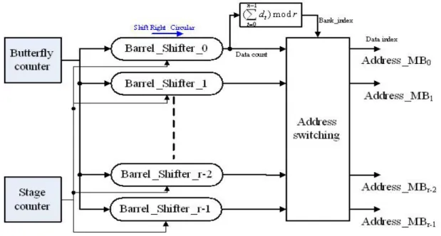
(45) In this design, the memory data allocation must be assigned to a four-bank memory block. Therefore, the conflict-free memory access method as discussed in section 3.1.1 is also implemented here. The new data address in each memory bank can be obtained by shifting the original data address right by two bits, which is easy to implement. On the other hand, the required bank index should be obtained by performing on-line summation and module 4 of one-dimension data address. In our FFT operation design, there are four different configurations linking the desired data access port index to the data memory bank index according to the memory addresses as shown in Table 3.6. For the “radix-2-mode”, the four configurations are identical with the “radix-22-mode”, if the location of “B” exchanges with “C”. When one bank index correspond to one data address at a specific port is given, we can select the compatible commutator configuration to redirect the data and the addresses buses. In another word, we only need to compute the mapping case of the data address <s> instead of calculating each bank index for each data address. Furthermore, the summation and module 4 value of the address <s> and that of the butterfly counter content are equal, because the value of <s> is obtained by inserting digit 0 into butterfly counter. The commutator configuration can be computed first before the data address is obtained. The architecture of the bank index generator to perform summation and module 4 is shown in Fig. 3.10. The obtained signals S1 and S0 decide the configuration in Table 3.5. The block “summation_mod4” in the figure is constructed by half adder and sum-generation subcircuit of full adder.. 35.
(46) Table 3.5 Four different configurations linking the desired data to the proper data memory bank Commutator configuration Commutator configuration S1 S0. for “radix-2-mode”. 2. for “radix-2 -mode” (The first stage of non-power-of-4 point). 0. 0. 1. 1. 0. 1. 0. 1. Desired write data order. Data order in memory banks. Desired read data order. Desired write data order. Data order in memory banks. Desired read data order. D. D. D. D. D. D. C. C. C. C. B. C. B. B. B. B. C. B. A. A. A. A. A. A. Desired write data order. Data order in memory banks. Desired read data order. Desired write data order. Data order in memory banks. Desired read data order. D. C. D. D. B. D. C. B. C. C. C. C. B. A. B. B. A. B. A. D. A. A. D. A. Desired write data order. Data order in memory banks. Desired read data order. Desired write data order. Data order in memory banks. Desired read data order. D. B. D. D. C. D. C. A. C. C. A. C. B. D. B. B. D. B. A. C. A. A. B. A. Desired write data order. Data order in memory banks. Desired read data order. Desired write data order. Data order in memory banks. Desired read data order. D. A. D. D. A. D. C. D. C. C. D. C. B. C. B. B. B. B. A. B. A. A. C. A. 36.
(47) B u tte rfly c o u n te r [1 1 :0 ]. [1 1 :1 0 ]. [9 :8 ]. [7 :6 ]. [5 :4 ]. [3 :2 ]. s u m m a tio n _ m o d 4. s u m m a tio n _ m o d 4. s u m m a tio n _ m o d 4. [1 :0 ]. s u m m a tio n _ m o d 4. s u m m a tio n _ m o d 4. S0. S1. A. B. s u m m a tio n _ m o d 4. 2. 2 B1. A1. B0. s u m -g e n e ra tio n s u b c irc u it o f fu ll adder. A0. H a lf a d d e r. S1. S0. S. Fig. 3.10 Block diagram of memory bank index generator. The coefficient index generator of the variable-length FFT processor is similar to that of the fixed-length FFT processor. The block diagram as shown in Fig. 3.11 just integrates the architecture of Fig. 3.3 and the controller of stage counter and butterfly counter of Fig. 3.9. Besides the index value of WNn, the index value of WN2n, WN3n, and WNn+(N/4) required by radix-22/2 butterfly PE are computed at the same time.. 37.
(48) Sym bol Length. 2. 1 Radix-2 2 /R adix-2 M ode selector. 1. Initial stage. MUX. +. + MUX. Stage finish controller. B utterfly counter [11:0]. reset. MUX Stage counter [2:0]. Barrel Shifter. <<1. N /4 M UX. + Coefficient index 2n. C oefficient index 3n or n+(N /4). C oefficient index n. Fig. 3.11 Block diagram of the variable-length coefficient index generator. 3.1.4 Comparison Comparisons of the mentioned three kinds of the variable-length data address generators are shown in Table 3.6, where the results are synthesized by UMC 0.18µm standard cell library with Synopsis Design Analyzer in 200MHz operating clock. The design involves various FFT lengths including 8192, 4096, 2048…, 512 and 256 points.. Table 3.6 Comparison of the variable-length data address generators Total gate counts The proposed architecture ( Fig. 3.9 ). 735. Hung’s design ( Fig. 3.6 ). 1246. Chang’s barrel shifter design ( Fig. 3.5 ). 1361 (the gate counts of the total barrel shifters are 763). 38.
(49) 3.2 Twiddle Factor Generation In the past, twiddle factor generation techniques were ignored due to the fact that OFDM systems were not as popular as they are now. Numerous FFT designs are devoted to efficient realization of the core FFT architecture and butterfly design. In general, the required twiddle factors are assumed stored in memories in advance and retrieved for butterfly multiplication whenever necessary. This usually ends up with a very large lookup table in comparison with the core FFT processing elements, especially for large FFT lengths such as 8192-point. Therefore, an efficient twiddle factor generator with small area and high speed performance is indispensable, particularly for portable and high data rate design such as OFDM systems. Many popular generation techniques for trigonometric functions can be applied to twiddle factor generation. Those computing techniques are mostly used for the designs of direct digital frequency synthesizer (DDFS). They include CORDIC algorithms, polynomial-based approach [22-28], recursive function generators [29], [30], and the most popular ROM-based table-lookup scheme [27]. The conventional CORDIC-based twiddle factor generations are by-products from the operations of the CORDIC-based processing element. Consequently, there is no need to generate the twiddle factor essentially. It is the biggest advantage of CORDIC-based FFT processor. In addition, it is realized by simple shift-and-add operations. We will propose a new CORDIC algorithm with on-line scale factor compensation, and we will detail it in chapter 4.. 39.
(50) 3.2.1 ROM-based Twiddle Factor Generator The twiddle factor is a complex value that consists of the cosine value in real part and the sine value in imaginary part. In addition, we can use the advantage of the quarter-wave symmetry of a sine/cosine value to reduce the ROM size to one- fourth. This means that only sine/cosine values from 0 to π/2 have to be stored. Furthermore, one can only store sine and cosine values from 0 to π/4 in ROM by using eight wave symmetry of a sine and cosine value. And the values of all regions can be reconstructed by only 1/8-period sinusoidal and cosine waveforms. This approach corresponds to Fig. 3.12 and Table 3.7.. Fig. 3.12 Wave symmetry of a sine and cosine value Table 3.7 Reconstruct the values of all regions by 1/8-period sine/cosine I. II. III. IV. V. VI. VII. VIII. real. A. B. −B. −A. −A. −B. B. A. imaginary. B. A. A. B. −B. −A. −A. −B. 40.
(51) The ROM-based table-lookup method is the simplest and most popular approach for twiddle factor generation. It is good for short-length FFT computation, such as 64-point FFT in 802.11a. However, the table size will grows intolerably large for large FFT lengths such as 8192-point FFT in the DVB and VDSL systems.. 3.2.2 The Proposed Recursive Twiddle Factor Generator The twiddle factors can be efficiently generated by using the polynomial-based DDFS [22-28], which are based on the concept of piecewise polynomial approximation to a function value. They ordinarily need memory space for the storage of polynomial coefficients and/or some function values, and some multiplication and addition operations to generate an output function point. However, the complexities of polynomial-based algorithms will grow with the output precision significantly. If a higher output precision is desired, a higher computation complexity will be required. The twiddle factor generator can also be realized with recursive function. The recursive sine function generator [29] is based on the well-known recursive feedback difference equation for the computation of sine and cosine functions. The approach’s key advantage is low complexity. For combined sine and cosine function generations, the approach only needs two multiplication and two addition operations per output point, which is less complicated than the mentioned table-lookup and polynomial designs. However, its serious drawback is the introduced error propagation problem in finite-precision computation, due to its error feedback character. Al-Ibrahim [30] proposed a solution to alleviate the error-propagation problem. However, this approach needs two extra multiplications and corresponding area to correct the propagation error.. 41.
(52) By considering the low-complexity merit of the recursive sine function generator, we attempt to reduce its main drawback of error-propagation problem with low overhead [21]. We will first analyze the error propagation bound of this approach and derive two error correction tables (for both sine and cosine functions), for the compensation the propagated finite-precision error. In all, the new design needs two constant multipliers and two adders to calculate these two functions. The correction table entries are at most three bit long, regardless of output word lengths. As a result, the proposed design has a smaller area than those mentioned designs in most cases. We will detail it as follows. Let’s first consider the generation of the imaginary part of a twiddle factor, that is, the sine function x[n] = (sinnθ)u[n]. In z-transform, one can get the following equation (3.10) [31]. ∞. H ( z ) = Ζ{[sin nθ ]u[n]} = ∑ (sin nθ )z − n = n=0. 1 ∞ jnθ (e − e − jnθ )z − n ∑ 2 j n=0. 1 1 1 (sin θ ) z −1 = ( − ) = , | z |> 1 2 j 1 − e jθ z −1 1 − e − jθ z −1 1 − 2(cosθ ) z −1 + z − 2. (3.10). From the result, the corresponding difference equations for the generation of sine function, and similarly the cosine functions are: sin nθ = 2 cosθ × sin(n − 1)θ − sin(n − 2)θ cos nθ = 2 cosθ × cos(n − 1)θ − cos(n − 2)θ. (3.11). There will introduce error propagation problem in finite-precision calculation due to the feedback terms of the previous generated output to the present output computation. The reduction method for finite-precision error propagation in [30] needs extra multipliers, adders and computation. To achieve a low-complexity error correction, here we include two error correction tables to recover the full-precision outputs. To decide the word length of the correction tables, we first analyze the upper bound of the finite-precision error propagation as expressed in equation (3.12). 42.
(53) sin nθ = 2cosθ ⋅ sin(n − 1)θ − sin(n − 2)θ = 2(cosθ ± 2 − ( B +1) )[sin(n − 1)θ ± 2− ( B +1) ] − [sin(n − 2)θ ± 2− ( B +1) ] = sin nθ ± 2− B [sin(n − 1)θ ± cosθ ± 2 −1 ± 2− ( B +1) ]. (3.12). where cos θ, sin (n − 1 )θ, sin (n − 2 )θ are finite - precision value of cos θ, sin (n − 1 )θ , sin (n − 2 )θ , respectively, with B - bit fractional precision. Therefore, the maximum error is bounded by:. max 2− B [sin(n − 1)θ ± cosθ ± 2−1 ± 2− ( B +1) ] < 2− ( B − 2). (3.13). This result shows a maximum two-bit error. Similar analysis results can be obtained with the cosine function. From this result, we can conclude an error correction word of three-bit long per output point. Specifically, in every iteration cycle, we will replace the 3 LSB’s of the currently generated output with the correction value stored in the correction tables. As a result, there will be no error propagation problem, and all the generated twiddle factors will be guaranteed full B-bit precision. In all, we need two tables (one for cosine and the other for sine values) of 3×N/8 bits each for total N twiddle factor values in the angle range of 0 to 2π. The factor 1/8 is due to table redundancy reduction by considering the symmetric property of trigonometric functions. This greatly reduces the required table size. Figure 3.13(a) shows the architecture of the proposed generator for the real part (the cosine function) of a twiddle factor. The same structure can be obtained for the imaginary part (the sine function), except that an additional table for the initial sine values sinθ should be included. Since both sine and cosine generators are exactly the same, they can be also combined as one interleaving structure by including simple control, a few registers, and a MUX after the correction-table stage, as shown in Fig. 3.13(b). 43.
(54) (a) Architecture of the proposed generator for real part (cosine) of a twiddle factor. (b) Combined twiddle factor generator architecture for interleaving computation of real and imaginary parts Fig. 3.13 Architecture of the proposed twiddle factor generator. Considering the radix-2 DIF N-point FFT as an example, where N=2k, operation steps of the proposed design can be summarized as: (1) Set the FFT stage number k=0. (2) Set the FFT subgroup number i=0, within the k-th stage. (3) Set the Initial values sin nθ = 0 and cos nθ = 1 , n=0, and output the twiddle factor values to the FFT processing element. 44.
(55) (4) Load cosθ = cos(2π / M ) and sin θ = sin(2π / M ) from a small table of. size of K-2=(log2N)-2 words, where M=N/2k. Output the twiddle factor values to the FFT processing element. Set the twiddle factor sequence number n=2. (5) Compute the finite-precision sin nθ and cos nθ according to equation (3.11). Replace the 3 LSB’s of sin nθ and cos nθ with the corresponding 3 LSB correction bits retrieved from the correction table. (6) Output the corrected sin nθ and cos nθ values to FFT processing element for twiddle factor multiplication. (7) If n < M-1, then n = n+1, go to step (4), otherwise proceed to the next step. (8) If i<k, i=i+1, go to step (3); otherwise, k=k+1. (9) If k<K, go to step (2); otherwise end of the twiddle factor computation.. 3.2.3 Comparison Table 3.8 is the simulation results of the proposed twiddle factor generator for N-point FFT operations with 16-bit output precision, where N=64, 256, 512, 1024, 2048, 4096, and 8192. The synthesized total gate counts and delays are based on UMC 0.18 µm standard cell library, subject to the maximum delay constraint of 5ns. From this table, since the areas and delay times increase very slowly with the increasing FFT lengths, we can conclude that both areas and delay are dominated by multipliers. The areas taken by correction tables are relatively insignificant. The synthesized small table size results are partially contributed by efficient EDA optimization process in synthesizing the table with combinational logic cells. Moreover, since our design costs the least multipliers among the existing designs (except for the table-lookup approach), we will expect a good area performance, compared with other 45.
數據
+7
相關文件
Promote project learning, mathematical modeling, and problem-based learning to strengthen the ability to integrate and apply knowledge and skills, and make. calculated
NETs can contribute to the continuing discussion in Hong Kong about the teaching and learning of English by joining local teachers in inter-school staff development initiatives..
Wang, Solving pseudomonotone variational inequalities and pseudocon- vex optimization problems using the projection neural network, IEEE Transactions on Neural Networks 17
Define instead the imaginary.. potential, magnetic field, lattice…) Dirac-BdG Hamiltonian:. with small, and matrix
Monopolies in synchronous distributed systems (Peleg 1998; Peleg
Corollary 13.3. For, if C is simple and lies in D, the function f is analytic at each point interior to and on C; so we apply the Cauchy-Goursat theorem directly. On the other hand,
Corollary 13.3. For, if C is simple and lies in D, the function f is analytic at each point interior to and on C; so we apply the Cauchy-Goursat theorem directly. On the other hand,
* School Survey 2017.. 1) Separate examination papers for the compulsory part of the two strands, with common questions set in Papers 1A & 1B for the common topics in
