Design and Implementation of an FPGA-Based
Control IC for AC-Voltage Regulation
Shih-Liang Jung,
Member, IEEE,Meng-Yueh Chang,
Student Member, IEEE,Jin-Yi Jyang, Li-Chia Yeh, and Ying-Yu Tzou,
Member, IEEEAbstract— This paper presents a field-programmable gate ar-ray (FPGA)-based control integrated circuit (IC) for controlling the pulsewidth modulation (PWM) inverters used in power-conditioning systems for ac-voltage regulation. We also propose a multiple-loop control scheme for this PWM inverter control IC to achieve sinusoidal voltage regulation under large load variations. The control scheme is simple in architecture and thus facilitates realization of the proposed digital controller for the PWM inverter using the FPGA-based circuit design approach. Bit-length effect of the digital PWM inverter controller has also been examined in this paper. The designed PWM inverter control IC has been realized using a single FPGA XC4005 from Xilinx, Inc., which can be used as a coprocessor with a general-purpose microprocessor in application of ac-voltage regulation. Owing to the high-speed nature of FPGA, the sampling frequency of the constructed IC can be raised up to the range that cannot be reached using a conventional digital controller based merely on microcontrollers or a digital signal processor (DSP). Experimen-tal results show the designed PWM inverter control IC using the proposed control scheme can achieve good voltage regulation against large load variations.
Index Terms—Digital control, FPGA, PWM inverter, UPS.
I. INTRODUCTION
T
HE CLOSED-LOOP-regulated pulsewidth modulation (PWM) inverters with filters have found their widespread applications in ac power-conditioning systems, such as automatic voltage regulators (AVR’s), programmable ac power sources, and uninterruptible power supplies (UPS’s). Owing to the proliferation of computer systems and the increasing awareness to protect critical information, the demand for UPS has grown tremendously. One basic function of a UPS is to convert the dc voltage of backup batteries to ac voltage with specified amplitude and frequency [1]. In the UPS applications, the PWM inverter is required to synthesize a sinusoidal waveform at its output port under different types of load. Since the PWM inverter plays such an important role in converting dc voltage to ac voltage, the performance of an ac power-conditioning system is highly dependent on closed-loop control of the built-in PWM inverter.Manuscript received October 8, 1997; revised August 31, 1998. Recommended by Associate Editor, D. Tan.
The authors are with the Power Electronics and Mechatronics Con-trol Laboratory, Department of Electrical and Control Engineering, National Chiao Tung University, Hsinchu, Taiwan, R.O.C. (e-mail: [email protected]; [email protected]; [email protected]; [email protected]@cc.nctu.-edu.tw; [email protected]@cc.nctu.-edu.tw; http://www.-pemclab.cn.nctu.edu.tw).
Publisher Item Identifier S 0885-8993(99)03748-5.
To minimize the harmonic distortion of the output waveform of a PWM inverter, many methods based on modulation strategies have been proposed [2], [3]. Though these methods have good steady-state characteristics, they are not suitable for the applications with sudden load change due to their open-loop control scheme. Good output-voltage regulation of a PWM inverter can only be solved by using closed-loop control techniques. Many closed-loop control schemes based on analog techniques have been proposed to improve the transient response of the PWM inverters under load variation at the expense of complex control circuitry [4], [5]. To further improve output performance, current-loop-regulated PWM inverters with output-voltage compensation have been proposed [6]–[8]. These kind of control schemes employed an inner current loop together with an outer voltage loop to split the pair of undamped poles caused by the resonance of an output filter so that the closed-loop system can achieve stable and fast dynamic response. Such multiple-loop schemes have been proved to be useful in power-conditioning systems for ac-voltage regulation.
With successively improving reliability and performance of microprocessors, digital control techniques have predom-inated over their analog counterparts in the past decade. Microprocessor-based digital control schemes have been ap-plied to the closed-loop regulation of the PWM inverters for sinusoidal waveform synthesis [9]–[11]. Microprocessor-based control schemes have the advantages of flexibility, higher reliability, and lower cost. If the multiple-loop schemes men-tioned above are to be realized by a microprocessor, however, most of the computation source will be devoted to inner current-loop control algorithm and generation of PWM gating signals. Only a limited computation resource will be left for other control loops and functions. Moreover, the demanding control requirements of modern power-conditioning systems will overload most general-purpose microprocessors. Though the multiprocessor scheme can deal with this problem, it costs more than the benefit it brings. Therefore, the engineers turn to the technology of ASIC and hope that the high-speed hard-wired logic can enhance the computation capability and thus relieve the load of microprocessors [12]–[14]. The ASIC-based technology provides a rapid and low-cost solution for special applications with large market. However, the longer development time and higher setup cost have made it improper for the products under R&D stage. Owing to the progress of technology, the life cycle of most modern electronic products becomes shorter than their design cycle. The need for fast
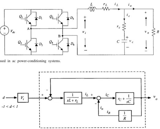
Fig. 1. PWM inverter used in ac power-conditioning systems.
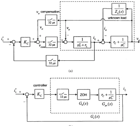
Fig. 2. Block diagram representation of the PWM inverter system.
prototyping is now growing up. The emergence of field-programmable gate array (FPGA) has drawn much attention due to its shorter design cycle, lower cost, and higher density. FPGA incorporates the architecture of gate arrays and the programmability of PLD’s. It comprises thousands of logic gates, some of which are grouped together as a configurable logic block (CLB) to simplify high-level circuit design. The interconnections between these logic gates are externally de-fined by SRAM or ROM. The simplicity and programmability of FPGA make it the most favorable choice for prototyping digital systems.
This paper presents an FPGA-based multiple-loop control scheme for the closed-loop regulation of a PWM inverter used for ac power conditioning. The proposed scheme contains an output-voltage decoupling mechanism so that the PWM inverter can achieve satisfactory ac-voltage regulation. In addition, a load disturbance compensation scheme has been developed to suppress the effect of load variation and thus improve the stiffness of the controlled PWM inverter. The proposed digital controller has been realized by an FPGA (XC4005) from Xilinx, Inc. The design and implementation of the FPGA-based control integrated circuit (IC) has been described in detail. The bit-length effect of the designed IC is also examined in this paper.
This paper is organized as follows. Section II derives the dynamic model of the PWM inverter system and describes the proposed multiple-loop control algorithm. Section III is concerned with the design and implementation of the FPGA-based control IC. Section IV examines the bit-length effect of the designed control IC. Section V shows the architecture of the experimental setup and gives some testing results. Section VI is the conclusion.
II. MULTIPLE-LOOP CONTROL OFPWM INVERTER A. Dynamic Model of the PWM Inverter
Fig. 1 shows the PWM inverter used in an ac power-conditioning system together with its output filter and load resistance. The full-bridge inverter, filter, and load are considered as the plant to be controlled. The voltage source serves as the dc bus and supplies power to the load through the inverter. The resistor is the equivalent series resistor (ESR) of the capacitor, while the resistor is the ESR of the inductor. According to the theory of state-space averaging and linearization, the characteristic equation of the PWM inverter shown in Fig. 1 can be derived as
(1) Fig. 2 depicts the block diagram representation of the PWM inverter system derived in (1). It shows the interconnection of major components of a PWM inverter. Since different types of load may be connected to the output of the PWM inverter, an ac power-conditioning system encounters significant load uncertainty. In order to maintain a sinusoidal output waveform under different loading conditions, a robust controller must be designed to regulate the PWM inverter. It can be observed from Fig. 2 that the dynamic model of the PWM inverter is similar to that of a permanent-magnet dc motor. Therefore, the concept of servo system design can also be adopted here to regulate the PWM inverter.
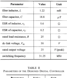
Fig. 3. Block diagram of the proposed digital control scheme.
(a)
(b) Fig. 4. Block diagram of (a) inner current loop and (b) simplified current loop.
Fig. 3 shows the proposed multiple-loop control scheme for ac-voltage regulation, where represents the load impedance connected to the PWM inverter. It can be seen from this figure that the output voltage behaves like a back electromotive force (emf) to the dc motor, and it disturbs the current loop. The load current also acts as a disturbance with respect to the outer voltage loop in a similar manner [8]. To cope with this problem, three signals are sensed as feedback in this control system: inductor current ( ), output voltage ( ), and load current ( ). The inductor current is sensed for the regulation of the current loop. The output voltage is sensed for ac-voltage regulation and “back EMF” compensation. The load current is sensed for rejecting the load disturbance.
B. Current-Loop Controller
Fig. 4(a) shows the model of the inner current loop of a PWM inverter. It can be seen that the output voltage ( ) acts
as an exogenous disturbance in this loop. The performance of the designed current-loop controller will be degraded if the interference of this disturbance cannot be well suppressed. To solve this problem, the current-loop control law is designed as
(2)
where is the current command generated by the outer voltage loop and is the computed control force applied to the PWM signal generator. It should be noted that the sensed output voltage ( ) has been added to the control law (2) so that the interference of the output voltage can be compensated. Owing to this compensation, the model of the inner current loop can be further simplified as shown in Fig. 4(b). The gain is designed through deadbeat control theory so that the root of the closed current loop can be placed at zero to achieve
(a)
(b) Fig. 5. Block diagram of (a) outer voltage loop and (b) simplified voltage loop.
deadbeat effect [15]
(3) Owing to the deadbeat effect of the designed current loop, the inductor current can respond to the current command as quickly as possible. This implies that the dynamics of the inductor can be well controlled and thus guarantees fast response.
C. Voltage-Loop Controller
Since the designed inner loop can follow the current com-mand faithfully due to its fast dynamics, it is reasonable to take the current loop as a constant gain in the design of the outer loop controller. Fig. 5(a) shows the block diagram of the outer voltage loop under this assumption. The corresponding voltage-loop control law is
(4) where is the voltage reference and is the computed current command for the inner current loop. Since the load dynamics are unknown, the load current acts as a disturbance with respect to the outer voltage loop. Therefore, we take the load current as feedback signal and add it to the control law (4) to remedy the defect caused by load disturbance. With this term, the outer voltage loop can be further simplified as shown in Fig. 5(b). Similarly, the gain is designed through deadbeat theory as follows:
(5)
TABLE I
PARAMETERS OF THEPWM INVERTER
TABLE II
PARAMETERS OF THEDESIGNEDDIGITALCONTROLLER
The relevant parameters of the PWM inverter and the designed digital controller are listed in Tables I and II, respectively.
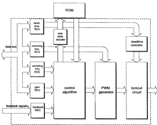
Fig. 6. Functional block diagram of the designed IC.
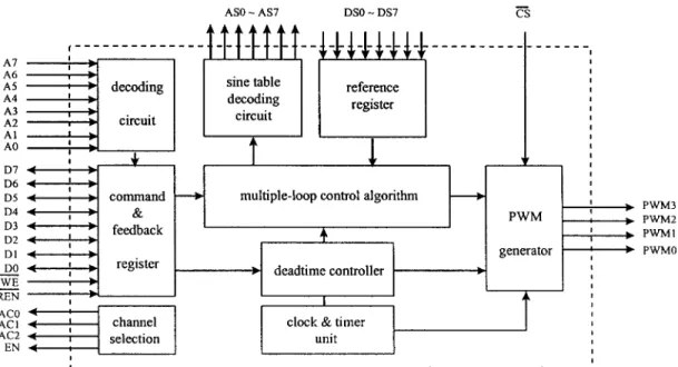
III. DESIGN OF THEFPGA-BASED CONTROL IC FPGA has become the main stream in complex logic circuit design due to its flexibility, ease of use, and short time to market [14]. The programmable hard-wired feature of FPGA provides a solution to the conflict between demanding computation requirements and cost. Therefore, it is beneficial to employ FPGA as part of a digital controller to relieve the microprocessor from time-consuming computations. In the application of ac power-conditioning systems, the control IC should function as a coprocessor with a general-purpose micro-processor to provide complete control and computer interface functions. Therefore, a built-in computer interface is necessary for the PWM inverter control IC. The microprocessor handles high-level operations such as power-on sequence control, power monitoring, parameter adaptation, self-calibration, and diagnosis, while the control IC takes charge of low-level real-time tasks such as feedback control, PWM waveform generation, and data acquisition.
As a digital signal processing unit, the most important issue in designing the control IC is the choice of numerical data processing scheme: floating-point or fixed-point arithmetic. Floating-point arithmetic gets it benefits of wide dynamic range and low round-off error, however, its hardware re-alization is much more complicated. Fixed-point arithmetic provides a more practical solution to most industrial appli-cations due to its simple circuit realization. However, proper numerical scaling plays a very important role in the synthesis of an integer controller. In this paper, 8-b arithmetic with external ROM-based sine-table reference is adopted to realize the PWM inverter control IC for ac-voltage regulation. This IC receives load current, inductor current, and output voltage from an analog–digital (A/D) converter as feedback signals, and the required pulsewidths for the PWM inverter are then computed
in accordance with the proposed multiple-loop algorithm and the sine reference from EPROM. Finally, the PWM signal with proper deadtime is generated and sent to the gate drive of the controlled PWM inverter.
Fig. 6 shows the functional block diagram of the designed control IC. It has five command registers for storing gains of the control loop ( and ), PWM switching frequency, sampling frequency, and the deadtime for the PWM gating signals. In order to simplify the hardware design, all these command registers are tied to a common data bus for com-puter interface and decoded by a command-mode decoder. To facilitate the acquisition of feedback information, three extra registers are designed for housing the data from A/D con-verters. A sine-table decoder is designed to generate address for fetching sine reference stored in an external EPROM. To obtain proper gating signals, a regulation controller is designed to figure out the required pulse width according to the reference command, the sensed feedback signals, and the multiple-loop algorithm proposed in the last section. To protect the switching devices from short circuit, a deadtime controller is included in the designed IC so that the generated PWM patterns can have proper delay time at each switching instant. Before designing the proposed multiple-loop controller, the switching frequency of the PWM inverter and the sampling frequency of each control loop must be determined so that the control parameters can be designed accordingly. In order to suppress the sideband harmonics, the switching frequency should be an integral multiple of the sampling frequency of the digital controller. In this paper, the relationship among these frequencies is set as follows:
(6) where is the PWM switching frequency of the inverter while
Fig. 7. Eight-bit approximate realization of the proposed multiple-loop control algorithm.
TABLE III
PARAMETERS SCALING OFKEYVARIABLES
and are the sampling frequencies of inner current loop and outer voltage loop, respectively. To obtain fast current response, the sampling frequency of inner loop is set equal to the switching frequency. Since the voltage response is slower than the current response, it is reasonable to set the sampling rate of outer loop as one half of that of the inner loop.
In our constructed PWM inverter system, the dc-link voltage is set as 50 V. Therefore, the actuating force must fall within the range of 50 V. Table III shows the scaling scheme of the relevant signals for the 8-b arithmetic operations. Because the current signal is much smaller than the sensed voltage signal, the current signal must be amplified by 32–40 times to fully employ the dynamic range of the feedback signals. Therefore, the sensed current signal must be rescaled as follows:
(7) The variables with a bar denote the values after scaling. To simplify the design, a virtual current-loop gain is defined as
(8)
Owing to the quantization effect of fixed-point arithmetic, the control gains cannot be realized precisely. The integer approximation of the a selected virtual current-loop gain, such as 37.8/40, can be expressed as
(9) Since all the terms are in the form of powers of 1/2, only data shift is necessary for the calculation of (9). The above approximation has an error of 0.79%, and it is acceptable in this application. In a similar manner, the voltage-loop control law is realized as
(10) A selected voltage-loop gain of 0.316 can be approximated as (11) The approximation error is about 1.11%. Fig. 7 shows the 8-b approximate realization of the proposed multiple-loop control algorithm.
The required pulsewidth of the gating signal is generated as follows:
(12) Bipolar pulsewidth modulation scheme, in which a duty of 50% means zero average at output, is employed in this application. Only 256 values can be realized from zero to full duty due to the 8-b resolution. Fig. 8 shows the block diagram of the PWM signal generator. To protect the switching devices from short circuit, a programmable deadtime controller is also included in the designed control IC.
TABLE IV
KEYCOMPONENTS, USINGDIFFERENTBIT-LENGTH REALIZATION
Fig. 8. Block diagram of the PWM generator.
IV. FINITE WORD-LENGTHEFFECT
Fixed-point arithmetic is typical in real-time digital con-trol systems. Numerical variables and parameters must be converted to approximate integers with finite word length. Therefore, it is necessary to investigate the effect of word length imposed on a digital control system. Since the cost of a hard-wired digital controller is directly related to the word length of the data bus, the best design would be the one with the shortest word length and one that also complies with all design specifications.
Fig. 9 shows the simulation results of the designed PWM inverter with different word length. It can be observed that better performance can be obtained if a longer word length is employed. Though 8-b data length exhibits a worse result, its performance is still acceptable in this application. Table IV illustrates the cost of critical elements and the effort in implementing the designed digital controller under different bit length. Only the devices relevant to the word length are counted in this table. All the devices listed have nearly the same specifications except the word size. For the 8-b case, the FPGA XC4005 with 196 CLB’s is sufficient to realize the proposed multiple-loop control scheme. While in the 12-b case, however, XC4010 with 400 CLB’s should be employed. It follows that the total cost of these key elements in 8-b real-ization is only about two fifths of that of 12-b realreal-ization as far as our application is concerned. Since the performance of 8-b realization can meet the essential requirement, the word length of the digital controller designed in this paper is thus set as 8 b.
V. HARDWAREREALIZATION AND EXPERIMENTALRESULTS
The proposed digital PWM inverter was implemented by an SRAM-based FPGA XC4005 from Xilinx, Inc. The XC4005 has 5000 logic gate, 196 configurable logic blocks (CLB’s),
(a)
(b)
Fig. 9. Simulation results of the designed PWM inverter with different bit lengths: (a) 8 and (b) 12 b.
and 112 input/output blocks (IOB’s). Xilinx also provides some CAD tools (Xilinx Automated CAE Tools, XACT) for the development of ASIC’s employing FPGA’s. XACT consists of a schematic entry editor, a cell library, an interface with the schematic entry editor, logic and timing simulation software, and design implementation software. The logic and timing simulation software is especially important for the design of complicated digital circuits because it is better to resolve circuit problems during the early design stage. Fig. 10 illustrates the timing simulation results of the developed con-trol IC. In designing an ASIC using FPGA’s, attention must be paid to the placement of logic blocks and the interconnection among them. The simplicity of the proposed control law
Fig. 10. Timing simulation of the developed control IC.
Fig. 11. Pin assignment of the constructed control IC.
also simplifies the work for interconnection routing. Fig. 11 illustrates the pin assignment of the constructed control IC.
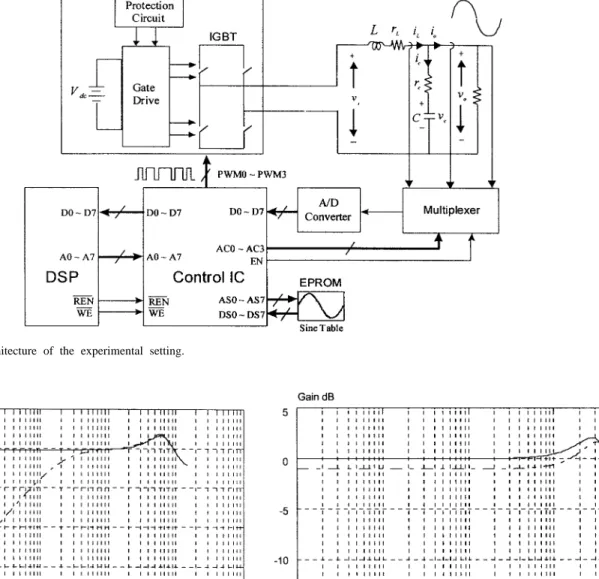
Fig. 12 shows the hardware architecture of the experimental system constructed in this paper. The developed control IC works as a coprocessor with a single-chip DSP controller (TMS320C14) from Texas Instruments. The DSP serves as a host processor and governs the work of tuning control parameters. The bitstream of the FPGA-based IC, which defines the interconnection among the CLB’s inside the FPGA, is stored in an EPROM. The bitstream will be loaded into the FPGA automatically after the power turns on. The loading
operation is similar to that of the BIOS in personal computers. The feedback signals are multiplexed before feeding into the 8-b A/D converter. The converted digital data is then sent to FPGA for further processing. The reference command of the digital control system is also stored in an external EPROM in the form of sampled sinusoidal waveform. Though a 512-point sine table is employed in the proposed control scheme, however, only 128 of them are stored in the EPROM due to the symmetry of the sinusoidal wave. The FPGA generates a PWM switching pattern according to the received data and the designed control logic.
Fig. 12. Hardware architecture of the experimental setting.
Fig. 13. Frequency response of the inner current loop. (Dashed: without output-voltage compensation. Solid: with output-voltage compensation.)
A built-in system clock (8 MHz) of the FPGA together with some counters can be used to set the PWM frequency of the power converter and the sampling frequency of the digital controller. The PWM frequency is set as 31.25 kHz, while the sampling frequency of the inner and outer control loops are set as 31.25 and 15.625 kHz, respectively. The high-speed programmable features of FPGA have made it possible to raise the sampling frequency up to the range that cannot be reached using conventional microprocessors.
Fig. 13 shows the frequency response of the designed inner current loop. It can be seen that the decoupling effect of the output-voltage compensation does have an enhancement on the robustness of the current-loop controller. The bandwidth of the designed inner loop reaches about 9 kHz, which is higher than using conventional digital control strategies. Owing to the wide bandwidth of the inner current loop, the outer voltage
Fig. 14. Frequency response of the outer voltage loop. (Dashed: closed loop without load current compensation. Solid: closed loop with load current compensation.)
loop can have better performance than the one without inner control loop. Fig. 14 shows the frequency response of the designed outer loop. It can be observed that the proposed load disturbance compensation scheme does improve the stiffness of the output voltage. The bandwidth of the outer voltage loop is about 4 kHz, which is high enough for line-frequency ac-voltage regulation.
Fig. 15 shows the measured waveform of the inductor current. It can be observed that the inductor current can follow the command faithfully. This implies that the dynamics of inductor has been well controlled by the proposed current-loop controller. Fig. 16 shows the output waveforms of the PWM inverter under phase-controlled load with a firing angle of 90 . The total harmonic distortion (THD) of the output voltage is
(a)
(b)
Fig. 15. Experimental results of the inductor current: (a) current command and (b) measured inductor current.
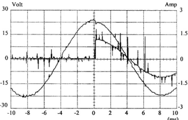
Fig. 16. Output voltage and load current under phase-controlled load.
about 2%. Although a nonlinear load has been connected, the output waveform can still be kept sinusoidal. The voltage drop at the instant of load variation can be quickly recovered within a short period of time. It can be seen from these results that the high-speed nature of FPGA has effectively extended the bandwidth of the controlled PWM inverter and improved the dynamic response of output voltage. It also shows that the
multiple-loop control scheme. The proposed control scheme incorporates an outer voltage loop with an inner current loop to regulate both the output voltage and inductor current of the PWM inverter. The design and realization aspects of the FPGA-based control IC have been described in this paper. The bit-length effect of the designed control IC, which provides some guidelines in determination of the word length, has also been discussed in this paper. A digital PWM inverter control system based on an FPGA XC4005 was constructed to verify the proposed control scheme. Owing to the highly integrated facility of the designed control IC, the complexity of the con-structed system can be tremendously reduced. Experimental results show that the controlled PWM inverter can sustain large load variations. The high-speed nature of the constructed control IC has effectively extended the bandwidth of the ac power sources up to the range that cannot be reached by the conventional digital control techniques based on DSP or microcontrollers.
REFERENCES
[1] D. C. Griffith, Uninterruptible Power Supplies: Power Conditioners for
Critical Equipment. New York: Marcel Dekker, 1989.
[2] G. S. Buji, “Optimum output waveforms in PWM inverters,” IEEE
Trans. Ind. Applicat., vol. IA-16, no. 6, pp. 830–836, 1980.
[3] I. J. Pitel, S. N. Talukdar, and P. Wood, “Characterization of pro-grammed waveform pulse width modulation,” IEEE Trans. Ind.
Appli-cat., vol. 16, no. 5, pp. 707–715, 1980.
[4] Y. Sekino, M. Shibata, and N. Hotaka, “Inverter output voltage wave-form closed-loop control technique,” in IEEE INTELEC Conf. Rec., 1983, pp. 205–212.
[5] A. Nabae, H. Nakano, and Y. Okamura, “A novel control strategy for inverter with sinusoidal voltage and current outputs,” in IEEE PESC
Conf. Rec., 1994, pp. 154–159.
[6] T. Kawabata, Y. Shikano, and S. Higashino, “Chargerless UPS us-ing multi-functional BIMOS inverter—Sinusoidal voltage waveform inverter with current minor loop,” in IEEE IAS Annu. Meeting Conf.
Rec., 1986, pp. 513–520.
[7] N. M. Abdel-Rahim and J. E. Quaicoe, “Analysis and design of a multiple feedback loop control strategy for single-phase voltage-source UPS inverters,” IEEE Trans. Power Electron., vol. 11, no. 4, pp. 532–541, 1996.
[8] M. J. Ryan and R. D. Lorenz, “A high performance sine wave inverter controller with capacitor current feedback and ‘back-EMF’ decoupling,” in IEEE PESC Conf. Rec., 1995, pp. 507–513.
[9] A. Kawamura, T. Haneyoshi, and R. G. Hoft, “Deadbeat controlled PWM inverter with parameter estimation using only voltage sensor,” in
IEEE PESC Conf. Rec., 1986, pp. 576–583.
[10] Y. Nishida and T. Haneyoshi, “Predictive instantaneous value controlled PWM inverter for UPS,” in IEEE PESC Conf. Rec., 1992, pp. 776–783. [11] S. L. Jung and Y. Y. Tzou, “Discrete sliding-mode control of a PWM inverter for sinusoidal output waveform synthesis with optimal sliding curve,” IEEE Trans. Power Electron., vol. 11, no. 4, pp. 567–577, 1996. [12] J. M. Retif, B. Allard, X. Jorda, and A. Perez, “Use of ASIC’s in PWM techniques for power converters,” in IEEE IECON Conf. Rec., 1993, pp. 683–688.
[13] R. C. Seals, “Position feedback control with a ‘smart’ controller based on an FPGA,” in IEE Colloquium on Stepper Motors and Their Control, 1994, pp. 6/1–6/3.
[14] W. S. Carter, “The future of programmable logic and its impact on digital system design,” in IEEE Int. Conf. Computer Design: VLSI in
Computers and Processors, 1994, pp. 10–16.
[15] S. L. Jung, H. S. Huang, M. Y. Chang, and Y. Y. Tzou, “DSP-based multiple-loop control strategy for single-phase inverters used in ac power sources,” in IEEE PESC Conf. Rec., 1997, pp. 706–712.
Shih-Liang Jung (S’93–M’98) was born in Hsinchu, Taiwan, R.O.C., on September 15, 1969. He received the B.S. and Ph.D. degrees in control engineering from National Chiao Tung University, Hsinchu, in 1991 and 1996, respectively.
From 1996 to 1997, he was a Post-Doctoral Research Fellow at National Chiao Tung University. He joined the army for military duty and has been an Instructor at the training center of the Military Integral Communication Command (MICC) since July 1997. His research interests include variable structure systems, DSP-based digital control techniques, control of power electronic systems, and microwave communication systems.
Meng-Yueh Chang (S’94) was born in Nantou, Taiwan, R.O.C., in 1968. He received the B.S. degree from National Cheng Kung University in 1991 and is currently working toward the Ph.D. degree in control engineering at National Chiao Tung University, Hsinchu, Taiwan.
His research interests are in the areas of power electronics. His recent research is related to high-power-factor reversible rectifiers, uninterruptible power supply systems, programmable ac sources, and dynamic load simulators.
Jin-Yi Jyang was born in Taiwan, R.O.C., on December 17, 1971. He received the junior college degree in electrical engineering from the National Taipei Institute of Technology and the B.S. degree in electronic engineering from the National Taiwan Institute of Technology, Taiwan, in 1992 and 1996, respectively. He is currently a graduate student at the Department of Control Engineering, National Chiao Tung University, Hsinchu, Taiwan.
From 1992 to 1994, he joined the army and was a Second Lieutenant charged with communication affairs. His special interests now are FPGA control IC for motor drivers and DSP applications in power electronics.
Li-Chia Yeh was born in Taiwan, R.O.C., on November 10, 1973. He received the B.S. degree in control engineering from National Chiao Tung University, Hsinchu, Taiwan, in 1996. He is currently a graduate student at the Institute of Electrical and Control Engineering, National Chiao Tung University.
He was a Vice Chairman of the student society of Control Engineering, National Chiao Tung University, in 1994. His special research interest now is FPGA-based controller design applied in UPS systems and digital motion control systems.
Ying-Yu Tzou (S’81–M’88) was born in Taiwan, R.O.C., on February 13, 1956. He received the B.S. and M.S. degrees in control engineering from National Chiao Tung University, Hsinchu, Taiwan, and the Ph.D. degree in electrical engineering from the Institute of Electronics Engineering, National Chiao Tung University, in 1978, 1983, and 1987, respectively.
From 1980 to 1981, he was with the Electronic Research and Service Organization (ERSO) of the Industry Technology Research Institute (ITRI) as a Design Engineer in the Control System Department. From 1983 to 1986, he was with Microtek Automation, Inc., as a Project Manager for the development of a computer numerical controller (CNC) for machine tools. He is currently a Professor at the Department of Electrical and Control Engineering, National Chiao Tung University, and also serves as an industrial consultant for many local power electronics and automation companies. He was the Director of the Institute of Control Engineering during 1992–1994. His special interests now are sensorless ac drives, intelligent UPS, FPGA-based control IC’s for motor drives and power converters, and DSP applications in power electronics and motion control.