A CMOS Delta–Sigma True RMS Converter
Wei-Shinn Wey and Yu-Chung Huang
Abstract—Conventionally, monolithic electronics true rms con-verters are constructed by bipolar circuitry. This paper describes a new architecture based on delta–sigma (16) modulation to realize a low-cost rms converter in CMOS technologies, especially intended for handheld digital multimeters. The signal-to-quan-tization noise ratio as well as transfer characteristics of this architecture have been deduced to obtain initial design param-eters. The use of an indirect charge transfer technique makes the converter gain depend only on an on-chip capacitor ratio, reducing gain drift and offering good gain accuracy. Measured results show that this converter achieves a signal-to-noise ratio of 88 dB and a relative error of 0.2% for arbitrary inputs with a signal crest factor up to three. The signal bandwidth exceeds 50 kHz, and the full-scale input range is greater than 0.4 Vrms. Without trimming and calibration, this converter has an absolute gain error less than 0.4%. This chip is fabricated in a 0.8- m double-poly, double-metal CMOS process and occupies active area of 1 mm2.
Index Terms—CMOS analog integrated circuits, delta–sigma modulation, indirect charge transfer filter, multiplier-divider, rms-to-dc converter, switched-capacitor circuits, true rms con-verter.
I. INTRODUCTION
T
HE root-mean-square (rms) value of arbitrary signals is one of the important parameters in electronics measure-ments, especially for digital multimeters (DMM’s). With the great progress of VLSI technologies, most circuitry of a hand-held DMM has been integrated into a single CMOS chip except an rms converter. Therefore, to integrate a CMOS rms converter into a DMM chip tends to be urgent.A few DMM’s use a simple rectifier and an averaging circuit for ac measurements. These meters have to be calibrated to read the rms value, but this is correct only for a specified waveform. In contrast to the averaging circuit, true rms converters compute the rms value of a signal regardless of waveform. To realize this rms converter, we have two alternative methods: comparing and computing. The comparing method, based on a thermal principle [1] or an electrostatic principle [2], has offered a wide bandwidth and good accuracy, but this method requires extra processing steps and complex packages, resulting in high-cost converters. The computing method is based on analog signal processing or digital signal processing. Although the analog processing method using translinear property of bipolar cir-cuitry has led to elegant solutions [3]–[5], these converters are difficult to implement in standard CMOS processes. In addition, because an averaging capacitor appears across a based-emitter
Manuscript received July 14, 1999; revised October 28, 1999. This work was supported by Fortune Semiconductor Company, Ltd., Taiwan, R.O.C.
The authors are with Institute of Electronics, National Chiao-Tung University, Hsin-Chu 300, Taiwan, R.O.C.
Publisher Item Identifier S 0018-9200(00)00935-5.
junction whose resistance varies with signal level, the response time increases linearly as the input signal is reduced [6]. There-fore, the response time especially for a decreasing input is also an important issue in the bipolar converters. Furthermore, in the digital processing method [7], the rms value of an input signal is calculated by a digital computation unit after high-speed analog-to-digital (A/D) conversion. This converter, providing a fast response, is realized in a CMOS process. However, the digital computation unit occupies a large chip area and thus does not lead to a low-cost solution.
The use of delta–sigma modulators in both low-pass and band-pass A/D converters has shown promise for coping with the analog component limitations inherent in VLSI tech-nologies. Actually, if we take account of the reference input of a modulator, the output of this modulator can be interpreted as a ratiometric function plus quantization noise. From this point of view, the modulator acts like a divider, and is thus re-ferred to as a divider in this paper. In addition, applying the 1-bit digital output of a divider to control a polarity switch, an analog input signal can be converted to its positive or nega-tive value by this switch so that the polarity switch acts like a multiplier. Furthermore, combining a divider and a polarity switch, a multiplier-divider can be built. Consequently, true rms converter-based nonlinear analog signal processing can be constructed from the multiplier-divider [8].
In this paper, we describe a CMOS true rms converter for a low-cost integration in a handheld DMM chip. A new archi-tecture using modulation for realizing a CMOS rms con-verter is presented in Section II. Transfer characteristics and signal-to-quantization noise ratio (SQNR) of the architecture have been deduced to obtain initial design parameters. In Sec-tion III, performance limitaSec-tions in measurements, including crest factor, noise, linearity, and response time, are investigated to get design criteria. In Section IV, an indirect-charge-transfer (IDCT) filter for realizing an ultralarge time-constant (ULT) is designed to make the converter gain depend only on an on-chip capacitor ratio. Due to the excellent stability and good matching properties of poly-poly capacitors in double-poly, double-metal (DPDM) CMOS processes, the converter gain drift is limited and gain calibration is not required. A test chip based on the new idea was successfully realized in a 0.8- m DPDM CMOS process. Details of the circuit implementation are described in Section V and measured results are shown in Section VI, which demonstrates that the performance of this converter meets the requirement of handheld DMM’s.
II. ARCHITECTURE OFTRUE RMSCONVERTER
A. Dividers
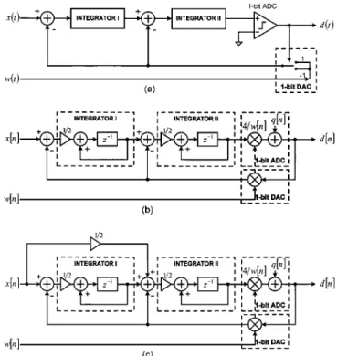
Fig. 1(a) illustrates a second-order divider, which features a numerator input a denominator input a
respectively, by a multiplier and by an additive quantization noise source [10]. Since the 1-bit ADC is sensitive only to the sign (not to the magnitude) of its input and is in the negative feedback loop including a multiplier, its additive noise model should be led by a factor of Thus, the divider output can be found by
(1) which shows a ratiometric function of the delayed numerator input to the denominator input and a difference equation of the quantization noise. It can be observed that the varying de-nominator makes the zeros of the noise transfer function be no longer at dc, and thus the SQNR of the divider is degraded by the quantization noise leakage in the interested frequency. The more rapidly the denominator varies, the more crucial the SQNR degradation becomes. To cope with this degradation, the de-nominator input should be restricted to vary slowly or its swing should be sufficiently small. Furthermore, if the denominator input is limited to be a quasi-static signal, which may vary in time but keeps static in steady state, the divider output can be simplified to
(2) where in steady state we have The mod-ulation noise now becomes the well-known second difference of [11]. In the rms converter application, the denominator will be fed by a quasi-static signal so that the SQNR degradation as (1) can be ignored and (2) can be used.
It is useful to construct a phase-compensated divider as shown in Fig. 1(c). A loop, referred to as a phase-compensation loop, feeding the numerator directly forward to the second inte-grator is added to compensate the phase delay resulting from the first integrator. The divider output can consequently be found by
(3) and thus the system function of this divider is given by
(4) Compared to a conventional second-order modulator [9], the quantization step size (referred to as of two should be
Fig. 1. Second-order 16 divider. (a) Block diagram, (b) sampled-data equivalent circuit, and (c) phase-compensated sampled-data circuit.
Fig. 2. Block diagram of16 multiplier-divider.
taken since the 1-bit output of the divider is treated as 1. There-fore, the spectral density of the modulation noise in (3) can be given by
(5) where is the sampling period.
B. Multiplier-Divider
A multiplier-divider is shown in Fig. 2. Depending on the divider’s output as 1 or 1, the multiplicand input is converted to or by the 1-bit multiplying DAC. In steady state, the DAC output can be given by
(6) It appears to be a multiplication-division function of the inputs and and an intermodulation function of and the shaped quantization noise. If the input contains any high-frequency component, the intermodulation yields impor-tant in-band noise components that will degrade the SQNR.
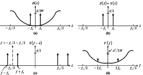
Fig. 3. Amplitude spectrum of the periodic convolution for the16 multiplier-divider. (a) Divider output. (b) Numerator and multiplicand inputs. (c) Mirrored and shifted spectrum of inputx[n]: (d) Multiplier-divider output.
Fig. 4. Block diagram of the16 true rms converter.
Therefore, should be restricted to be a band-limited signal to prevent this degradation.
In the rms converter application, the inputs and both are connected to a signal input so that Thus, the spectral density of can be found by
(7)
which corresponds to a periodic convolution. Assuming that is a sinusoidal input with frequency and amplitude the periodic convolution can be interpreted by Fig. 3(a)–(d). Plugging (4) and (5) into (7), the amplitude spectrum of can be found by
(8) If the 3-dB frequency of the low-pass filter is far less than the signal frequency so that the amplitude spectrum of
then can be given by
(9)
This equation will be used to obtain the SQNR of the rms converter.
C. trms Converter
As shown in Fig. 4, the proposed true rms (trms) converter is constructed from a multiplier-divider. The averaging filter has a very low 3-dB frequency to filter out all of the ac terms so that the filter’s output is an average response of its input. In ac measurements, a crest factor (CF) can be used to distinguish different waveforms having the same rms value. A crest factor is defined as the ratio of the peak signal amplitude to the rms amplitude (so that CF V /V , and it is always equal to or larger than one. Thus, to prevent the divider from over-load, a gain factor is placed on the feedback loop to keep the denominator of the divider always larger than the numerator. In addition, the multiplicand input is also scaled by the same factor to compensate the attenuated converter gain due to the feedback scaling. Therefore, the conversion accuracy is still maintained while measuring an input signal with a crest factor up to The converter output can be found by
(10) A true rms conversion is achieved where results from the signal delay of the divider and slightly depends on input wave-forms. For a sinusoidal input with signal frequency is given by
Fig. 5. SQNR plot of a second-order16 rms converter with a gain factor of three.
and the SQNR of this rms converter can be deduced from (9) and by
SQNR (12)
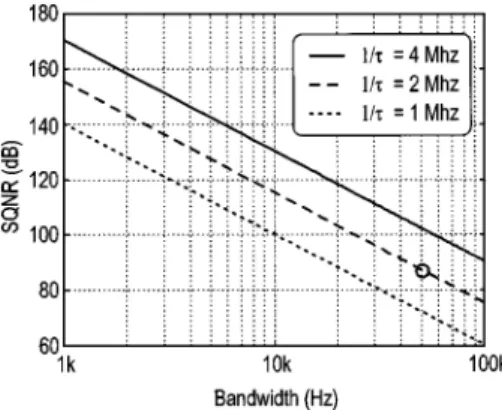
which depends only on the signal frequency regardless of the signal level, in contrast to modulators [9], [10], whose max-imum SQNR is achieved only while the modulator accommo-dates its largest input level. A plot of SQNR versus signal band-width of this converter is illustrated in Fig. 5.
III. LIMITATIONS OFMEASUREMENTPERFORMANCE
A. Crest Factor
A true rms converter computes the rms value of a signal with arbitrary waveforms. Waveforms differ in their crest factors. In this converter, a gain factor of can be designed to make the converter have the ability to accommodate an input signal having a crest factor of . However, taking a high gain factor en-larges the signal range of the operational amplifiers (op-amps) in the divider and degrades the SQNR of the converter from (12), resulting in sacrificing of the dynamic range. Consequently, to measure a greater crest factor signal or to obtain a larger con-verter dynamic range becomes a tradeoff. In this design, a gain factor of three is taken to maintain superior conversion accu-racy for an input signal with crest factor up to three.
B. Noise
Output noise of the rms converter restricts the smallest mea-surable input change of an ac measurement, which refers to the least-significant digit (LSD) of a meter’s display. A typical dis-play resolution of a handheld DMM is 4000 counts, resulting in a required rms converter that should have 100 V LSD and 400 mV full-scale input range. This corresponds to an output noise of 16 V to provide a noise-free indication. The
high oversampling ratio [13]. For example, assume that a 3-dB frequency of an averaging filter at Hz and a sampling frequency at MHz has an oversampling ratio of 200 000. Such a high oversampling ratio makes the in-band thermal noise far less than 16 V even for a sampling capacitor of 0.1 pF. Therefore, the output noise is dominated by quantization noise. Since the rms converter has the same SQNR for different input levels, a larger input signal will induce a greater quanti-zation noise. From (12) and Fig. 5, if a sampling frequency at 2 MHz and a signal bandwidth of 50 kHz are taken, an SQNR of 88 dB can be obtained. Assuming a full-scale input level of 400 mV the converter will have an output quantization noise of 16 V
C. Linearity
Since the robustness of modulators against circuit imper-fections has been proved in many other applications, linearity of the rms converter will be limited by component offsets and the 1-bit DAC with averaging filter. Component offsets usually do not introduce nonlinear distortion in most other applications, but they do in the rms converter due to the nonlinear feedback to the divider’s denominator input. Referring to Fig. 4, the input-re-ferred offsets of the numerator and the denominator of the di-vider are assumed to be and respectively, and that of the averaging filter is The input signal is expressed as a combined signal of and so that
(13) Then the output can be found by (14), shown at the bottom of the page. In pure ac measurements , the offset voltage is modulated into the ac band and hence is filtered out by the averaging filter. In contrast to , the offset volt-ages and induce nonlinear distortion in all measure-ments. It can be found that the nonlinear distortion becomes cru-cial for low-level input signals. Offset sources in switched-ca-pacitor (SC) circuits are op-amps and charge injections from MOS switches. These offsets can be reduced by using chopper op-amps and fully differential configuration, respectively. How-ever, residual offset [14] still remains and thus limits the lin-earity of this converter.
Furthermore, the linearity performance of the 1-bit multi-plying DAC with averaging filter also plays an important role to
Fig. 6. Simulated output response versus predicted single-pole, low-pass filter’s output response.
make this converter have good linearity. Several circuits to im-plement audio DAC’s have been revealed and explored by [15]. Due to lower sensitivity for clock jitter, it has been proved that circuitry based on charge packet transformation has supe-rior performance over others [16]. However, comparing with a postfilter for audio DAC’s, the averaging filter for rms con-verters has two more severe requirements: much lower 3-dB fre-quency and good gain stability. This will be discussed in the next section.
D. Response Time
The response time of the rms converter is limited by the aver-aging filter with ultralarge time constant. While a step signal is applied to the input of a single-pole filter with a 3-dB frequency the time needed for the output to reach a final value to within a specified tolerance can be given by
(15) Fig. 6 shows a simulated output response of the proposed rms converter with a 50-Hz filter applied by a step-decreasing signal from 1 V to 10 mV which is faster than that of a 50-Hz single-pole, low-pass filter. It can be found that the response time of this converter can be roughly estimated by (15). In a digital rms converter, the response time is restricted by a mean-squared filter with a low 3-dB frequency. For example, if the specified tolerance and 3-dB frequency are 0.005% and 3.5 Hz, respectively, from (15), the response time can be estimated to be 0.45 s, which is close to the time (0.42 s) depicted in [7]. Therefore, the response time of a delta–sigma rms converter is comparable to that of a digital one.
IV. ULTRALARGETIMECONSTANTSC FILTERS
To filter out all of the ac terms including the harmonics due to multiplication as well as the quantization noise, the 3-dB fre-quency of the averaging filter should be low enough (e.g., 5 Hz) in the rms converter. In addition, to obtain a sufficient high over-sampling ratio, the over-sampling frequency has to be much higher (e.g., 2 MHz) than the signal bandwidth. The two demands lead the averaging filter to have an ultralarge time-constant and the required capacitor spread to run into hundreds of thousands
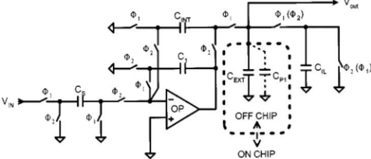
Fig. 7. Indirect charge transfer averaging filter.
(e.g. 400 000), resulting in a prohibitively large area require-ment. Some very large time-constant (VLT) SC filters have been proposed [17], [18]. The required capacitor spread has been re-duced to its square-root value, but these VLT filters still cannot serve for this spread requirement of hundreds of thousands. A previous design [19] aimed at the same goal uses external re-sistors and capacitors to realize a ULT filter [20]. However, the converter gain in this work depends not only on a capacitor ratio but also on a sampling frequency, resistance value, and capac-itance value. Due to the different temperature coefficients be-tween the capacitors and the resistors, the gain drift becomes a crucial issue. Moreover, the tolerance of the absolute value of capacitance in VLSI technologies is usually above 10%; thus, gain calibration is indispensable to the previous work.
In CMOS technologies, the accuracy of capacitor ratio better than 0.1% can be performed by unit and common-centroid pacitor layouts [21]. Besides, the temperature stability of a ca-pacitor ratio achieving 2 ppm/ C has been shown by a trans-ducer ADC [13]. Thus, it is preferred to construct an averaging filter whose dc gain depends only on a capacitor ratio in this ap-plication.
The approach taken here is to use an indirect charge transfer technique, demonstrated by Fig. 7. During the phase, a charge packet of the magnitude of is delivered to an integrating capacitor In phase, capacitors and are connected in parallel with each other, and hence the charge on and redistributes across the parallel combination. Since the capacitance of the external capacitor is usually far greater than that of most of the charge on flows into That is, the charge packet sampled on is indirectly transferred to via A capacitor serves as a voltage source, so the op-amp output does not have to move much during this phase. Besides, an internal load capacitor is charged to the voltage during (or phase and is discharged to ground voltage
(or ) phase, respectively. Thus, the transfer function of the IDCT filter can be derived by
(16) whose dc gain and 3-dB frequency are, respectively, given by
Fig. 8. Fully differential 1-bit multiplying DAC with an IDCT filter.
Fig. 9. Clock timing diagram.
and
(18) where A dc gain depending only on an on-chip capacitor ratio is performed.
V. CIRCUITIMPLEMENTATION
A fully differential configuration is used in the implemen-tation to not only maximize dynamic range but also suppress common-mode noise such as digital noise coupling through the common substrate and power lines. This also leads to a first-order cancellation of the charge injection offsets from switches, having another benefit of reducing the low-level signal distor-tion as seen in (14). The common-mode feedback (CMFB) for each fully differential op-amp is provided by a SC dynamic CMFB circuit, which has an advantage of consuming minimum power [22].
A 1-bit multiplying DAC with the averaging filter can be built by combining the IDCT filter with 1-bit multiplying switches controlled by the digital input signal , as shown in Fig. 8. The control clock is a nonoverlap two-phase clock, as illustrated in Fig. 9. Both delayed clock phase and are taken to make charge injection errors from CMOS switches become signal-in-dependent [23]. During the phase, the input voltage is sam-pled onto the capacitors During the phase, depending on the 1-bit digital input ’s being 1 or 1, the charge packet of the magnitude of either or is delivered
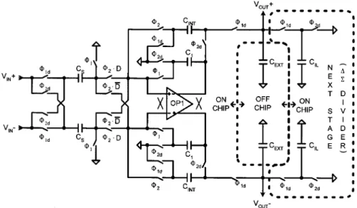
to an integrating capacitor Since the input is sam-pled two times in each clock cycle, this filter has a dc gain of 2 The internal-load capacitors here are the de-nominator sampling capacitors of the divider stage, and the large capacitors are off-chip to make the 3-dB frequency low enough. In addition, the op-amp offset is reduced by the chopper-stabilized technique in [12], [14].
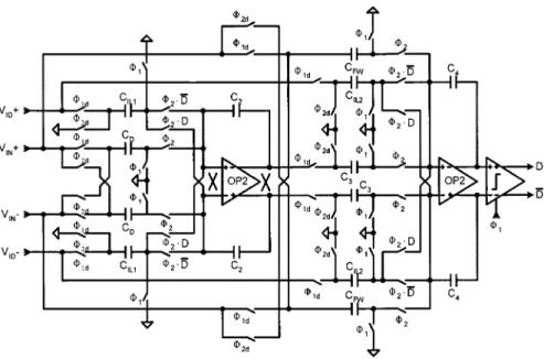
Fig. 10 illustrates a schematic of the phase-compensated divider as in Fig. 1(c). Each integrator has a gain coefficient of 0.5, and the op-amp of the first integrator is chopper-stabilized. The numerator input is sampled in both and phases to obtain an additional phase lead of a half of a sampling period. The SC network associated with feeding the input directly forward to the second integrator is designed to com-pensate the delay resulting from the first integrator. To perform this compensation, the capacitance value of should be half the value of A complete schematic of the rms converter is shown in Fig. 11, which features the divider as in Fig. 10, the 1-bit multiplying DAC with an IDCT filter as in Fig. 9, a clock generator, and two input buffers. The internal load capac-itor of the IDCT filter now is realized by the denominator sampling capacitors and The two chopper-stabilized input buffers are used to offer high input impedance. The output voltage can be found by
(19)
The converter gain depends on a capacitor ratio of
and where slightly depends on input waveforms. For a sinusoidal input, is identical to (11). Furthermore, it can be found that the response time is signal-level independent, in contrast to bipolar rms converters, which become slower at low input levels.
Since the crest factor is aimed at three, the gain factor of this converter is given by
Fig. 10. Fully-differential phase-compensated SC16 divider.
Fig. 11. Complete circuit description of the rms converter.
In a phase-compensated divider, we have , and thus the minimum capacitor is It has been investi-gated that noise can be neglected in this converter even for capacitance less than 0.1 pF. Therefore, the capacitor value of is chosen as 0.25 pF, and the other capacitor values can
be found by pF, pF, and
pF. In addition, if the external capacitor is given by
nF, the averaging filter has a 3-dB frequency of 5 Hz, from (18). All of the op-amps are Miller-compensated two-stage class A type [24]. Table I illustrates some important specifications of these op-amps. Because the op-amps BUF and OP1 are directly adopted from another design, the load capacitance (15 and 8 pF) they can drive are greater than the actual capacitance (9.5 and 5 pF, respectively) they should drive in this converter. Therefore, if the two op-amps are redesigned especially for this converter, the current consumption can be reduced.
The power consumed in a switched-capacitor circuit is gen-erally proportional to its integrators’ loading, and the minimum capacitance that could be used is restricted by noise. In addition, to measure input signals with crest factor of leads the required (internal) capacitor spread to be 2 Consequently,
TABLE I
SOME IMPORTANTCHARACTERISTICS OF THEOP-AMPS
the performance of power consumption is limited by the speci-fied crest factor and dynamic range. Compared to the traditional bipolar or digital converters [4], [7], this converter consumes more power. However, if power consumption becomes a major issue, it can be significantly improved by using a class AB am-plifier and dynamic biasing technique [22].
(a)
(b)
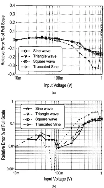
Fig. 12. Relative error percentage of full scale for 1-kHz various input waveforms. (a) Lineary-axis. (b) Logarithmic y-axis.
VI. EXPERIMENTALRESULTS
A test chip is fabricated in a 0.8- m DPDM CMOS process. The converter operates on 3-V supplies. A plot of relative error versus input levels of 1-kHz signals including sinusoidal wave, triangle wave, square wave, and truncated sine waves is shown in Fig. 12(a). The truncated sine waves have a signal crest factor of 2.41. For the specified full-scale range of 0.4 V this con-verter has a relative error of full scale less than 0.2%. Besides, to visualize the error at smaller input signals in a better way, an-other plot is illustrated in Fig. 12(b) whose -axis is plotted on a logarithmic scale.
In this chip, to observe the performance of the phase com-pensation, a pair of controllable switches is inserted into the phase-compensation loop of the divider to enable or disable the compensation. Measured frequency responses of this chip are shown in Fig. 13. While the compensation is disabled, the converter gain degrades rapidly for signal frequency greater than 20 kHz, which is very close to the theoretical prediction. In contrast to disabling the compensation, enabling it makes the converter have a flatter response whose gain error is less than 0.6% with 50-kHz bandwidth. Fig. 14 shows a frequency
Fig. 13. Frequency response of the converter with and without phase compensation.
Fig. 14. Frequency response of different signal levels.
Fig. 15. Measured converter gain variation in 20 samples.
response of the converter for different output levels. Signal degradation becomes noticeable while input level and signal frequency are less than 10 mV and greater than 50 kHz, respectively.
The converter gain is insensitive to process fluctuation since it depends only on an on-chip capacitor ratio. A histogram of measured gain variation in 20 samples is shown in Fig. 15. As shown in the histogram, no gain calibration is required; this
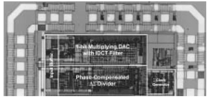
Fig. 16. Die microphotograph.
TABLE II
MEASUREDPERFORMANCESUMMARY
converter has an absolute gain error distributed in the range of 0.4%. Measured performance of this test chip is summarized in Table II. A die photograph is shown in Fig. 16 where the rms converter occupies an active area of 660 1480 m .
VII. CONCLUSION
One approach to realize a CMOS rms converter, a true rms converter, has been described and successfully integrated in a 0.8- m CMOS process. In a divider, a varying de-nominator degrades the SQNR of the divider. The maximum SQNR can be obtained by restricting the denominator to be a quasi-static signal. In addition, transfer characteristics of a rms converter has been investigated, showing that the SQNR of this converter depends only on the input signal frequency without regard to the input levels. The crest factor of this con-verter can be designed by changing a capacitor ratio. However, obtaining a higher crest factor is a tradeoff with the SQNR of this converter. Furthermore, the linearity of this converter is limited by residue offset, especially for low-level signals.
An IDCT filter has been developed to make the converter gain depend only on an on-chip capacitor ratio, so this converter has good gain accuracy and temperature stability. Experimental re-sults show that no trimming and calibration is required. This converter has an absolute gain error in the range of 0.4%. In addition, using the phase-compensation scheme has effectively enhanced the converter’s bandwidth. This converter has a band-width exceeding 50 kHz and a full-scale range greater than 0.4 V Furthermore, the relative error is 0.2% for arbitrary in-puts with a crest factor up to three. The response time of this converter is comparable to that of a digital converter, and the
consumed power could be reduced in the future design. There-fore, the presented converter is a good choice for further inte-gration of DMM chips.
REFERENCES
[1] A. W. van Herwaarden, H. P. Hochstenbach, and K. J. P. M. Harmans, “Integrated true RMS converter,” IEEE Trans. Instrum. Meas., vol. IM-35, pp. 224–225, June 1986.
[2] B. P. van Drieenhuizen and R. F. Wolffenbuttel, “Integrated microma-chined electrostatic true rms-to-dc converter,” IEEE Trans. Instrum.
Meas., vol. 44, pp. 370–373, Apr. 1995.
[3] B. Gilbert and L. W. Counts, “A monolithic RMS-DC converter with crest factor compensation,” in ISSCC Dig. Tech. Papers, Feb. 1976, pp. 110–111.
[4] R. F. Wassenaar, E. Seevinck, M. G. van Leeuwen, C. J. Speelman, and E. Holle, “New techniques for high-frequency RMS-to-DC conversion based on a multifunctional V-to-I converter,” IEEE J. Solid-State
Cir-cuits, vol. 23, pp. 802–815, June 1988.
[5] J. Mulder, A. C. van der Woerd, W. A. Serdijn, and A. H. M. van Roer-mund, “An RMS-DC converter based on the dynamic translinear prin-ciple,” IEEE J. Solid-State Circuits, vol. 32, pp. 1146–1150, July 1997. [6] B. Clark, M. Fazio, and D. Scoot, “RMS-to-DC converters ease
mea-surement tasks,” Analog Devices, Application Note AN-268, 1990. [7] E. J. van der Zwan, R. H. M. van Veldhoven, P. A. C. M. Nuijten, E. C.
Dijkmans, and S. D. Swift, “A 13 mW 500 kHz data acquisition IC with 4.5 digital dc and 0.02% accurate true-rms extraction,” in ISSCC Dig.
Tech. Papers, Feb. 1999, pp. 398–399.
[8] W. S. Wey and Y. C. Huang, “A delta-sigma true rms-to-dc converter using an indirect-charge-transfer filter,” in VLSI Circuits Dig. Tech.
Pa-pers, June 1999, pp. 93–94.
[9] J. C. Candy, “A use of double integration in sigma delta modulation,”
IEEE Trans. Commun., vol. C-33, pp. 249–258, Mar. 1985.
[10] R. M. Gray, “Oversampled sigma-delta modulation,” IEEE Trans.
Commun., vol. C-35, pp. 481–489, May 1987.
[11] J. C. Candy, “Oversampling methods for A/D and D/A conversion,” in
Oversampling Delta-Sigma Data Converters. New York: IEEE Press, 1992, pp. 1–25.
[12] K. C. Hsieh, P. R. Gray, D. Senderowicz, and D. G. Messerschmitt, “A low-noise chopper-stabilized differential switched-capacitor filtering technique,” IEEE J. Solid-State Circuits, vol. SC-20, pp. 1122–1132, Dec. 1985.
[13] D. McCartney, A. Sherry, J. O’Dowd, and P. Hickey, “A low-noise low-drift transducer ADC,” IEEE J. Solid-State Circuits, vol. 32, pp. 959–967, July 1997.
[14] C. C. Enz and G. C. Temes, “Circuit techniques for reducing the effects of op-amp imperfections: Autozeroing, correlated double sampling, and chopper stabilization,” Proc. IEEE, vol. 84, pp. 1584–1614, Nov. 1996. [15] F. O. Eynde and W. Sansen, “The practical implementation of sigma-delta D-to-A converters,” in Analog Interfaces for Digital Signal
Pro-cessing Systems. Norwell, MA: Kluwer Academic, 1993, ch. 5, pp. 217–248.
[16] P. Ju, K. Suyama, P. F. Ferguson, Jr., and W. Lee, “A 22-kHz multibit switched-capacitor sigma-delta D/A converter with 92 dB dynamic range,” IEEE J. Solid-State Circuits, vol. 30, pp. 1316–1325, Dec. 1995. [17] K. Nagaraj, “A parasitic-insensitive area-efficient switched-capacitor circuits,” IEEE Trans. Circuits Syst., vol. CAS-36, pp. 1210–1216, Sept. 1989.
[18] W. H. Ki and G. C. Temes, “Offset-compensated switched-capacitor in-tegrators,” in Proc. IEEE Int. Symp. Circuits and Systems, May 1990, pp. 2829–2832.
[19] W. S. Wey and Y. C. Huang, “A CMOS rms-to-dc converter using a16 multipler-divider,” in Proc. IEEE Int. Symp. Circuits and Systems, vol. II, May 1999, pp. 256–258.
[20] B. M. J. Kup, E. C. Dijkmans, P. J. A. Naus, and J. Sneep, “A bit-stream digital-to-analog converter with 18-b resolution,” IEEE J. Solid-State
Circuits, vol. 26, pp. 1757–1763, Dec. 1991.
[21] J. L. McCreary, “Matching properties, and voltage and temperature de-pendence of MOS capacitors,” IEEE J. Solid-State Circuits, vol. SC-16, pp. 608–616, Dec. 1981.
[22] R. Castello and P. R. Gray, “A high-performance micropower switched-capacitor filter,” IEEE J. Solid-State Circuits, vol. 20, pp. 1122–1132, Dec. 1995.
[23] P. W. Li, M. J. Chin, P. R. Gray, and R. Castello, “A ratio-independent algorithm analog-to-digital conversion technique,” IEEE J. Solid-State
engineering.
His research interests are in the area of integrated circuits and systems with an emphasis on sensor in-terface, measurement, and mixed-mode circuits.