國 立 交 通 大 學
奈 米 科 技 研究所碩士班
碩 士 論 文
新穎側向閘極奈米線場效電晶體應用於
即時偵測生物感測器
Real-Time and Label-Free Detection of the
Biomolecules with a Novel Side-Gated SiNW-FET
Biosensor
研 究 生: 夏德玲
Acknowledgment
致謝的開頭當然要把位置留給柯博,感謝柯博這兩年來在學術以及態度上給 我的教誨,讓我在專業領域以及待人處事上能更進一步,再加上班長這個職務給 我的歷練讓我更能懂得”掌握大局;洞悉人心"。 感謝其昌、俊淇學長在實驗上的帶領以及幫忙,這兩年下來多謝你們的包容 讓我能夠順利的交出論文順利的畢業; 感謝坤霖、老鼠學長在我剛進實驗室帶我 認識二餐的環境; 志威學長的跳舞天份也是讓我印象深刻; 謝謝群芳、志杰、敬 雅在實驗上的協助; 最要感謝就是奕儂,從一起實驗一起玩樂一起熬夜,謝謝你 帶給我碩士生涯一段難忘的回憶~ 佳典!曾經一段不愉快讓我長大也讓我了解社會的現實面,謝謝你讓我們還 能回到最初簡單的相處,這兩年來你敎會我很多謝謝你。 吳中書!我們真是不打不相識~對吧?最想讓我說謝謝的~就是你,在我人生懵 懂時人生低潮時,都有你的參與。謝謝你總是用簡單的字句影響我,謝謝你願意 接納這樣壞脾氣的我,對你~我心裡真的有太多的感謝跟不捨。但你說好朋友不 講這種客套話,所以老話一句: 謝謝這裡有小胖;謝謝這裡有香皮。 魏大爺!你是我一進來這裡第一個交心的好朋友,到現在也都還是在我的心 裡重要的位置,第一次喝醉你就幫了我一個大忙Æ幫我遛狗。打從那時候起,我 就決定要跟你當好朋友,常常覬覦你的密閉小空間,我可是受到它不少恩惠唷。 哈!!你這個行動土地公真是讓我又羨慕又忌妒阿! 菲菲!在這裡的我會不會讓你失望了呢?我好像沒什麼資格可以當你學姐 了,不像從前可以給你很多專業上的幫助,倒是不成熟的我還需要你的幫忙跟陪 伴!很開心能跟你再續前緣,簡簡單單的欣賞你! 嗯牆!知道我在說你~不要轉頭!!第一眼看到妳就想把你折斷。哈哈!誰叫你那 麼瘦,謝謝你的到來讓我在這個實驗室增添許多笑料,聊的來是一種奇妙的緣分 不在乎時間的長短。期許你在實驗上的專業領域能有所成長跟突破! 正姐!你真是個讓我歎為觀止的一號人物阿!除了萬事通之外,你的好歌聲更 是讓我難忘,再加上你悶騷的個性,我想這個實驗室有了你會更多彩多姿。也謝 謝你的細心細膩,讓我在那段難熬的時間裡多了份溫暖的感覺! 當然還要感謝實驗室在不同領域中共同努力以及給予協助的夥伴們: 子銘 學長、依蓁、美榕、品麟、舜博、Sri、Jagan、京璋、柏軒、薏卉。沒有你們的 話,我想碩士生活會增添許多難關要過吧!!很開心在這裡能夠遇到你們。新穎側向閘極奈米線場效電晶體應用於即時偵測生物感測器
學生: 夏德玲 指導教授: 柯富祥 教授
國立交通大學奈米科技研究所碩士班
摘 要
感測元件與生物分子的連結應用在未來的疾病診斷是個重要且具發展性的 課題。在此篇論文中,我們選擇甲狀腺乳突癌症相關變異基因BRAFV599E 以及癌症 指標物甲型胎兒蛋白抗原來當作偵測目標。我們以半導體奈米線為元件基礎的裝 置做為新穎的生物感測器,可偵測的生物分子或是化學物種包括有低濃度化學成 分離子、小分子、抗原抗體反應、檢測蛋白質、DNA 和病毒。在我的研究裡,使 用了互補式金氧半場效電晶體的技術來製作新穎側向閘極場效電晶體生物感測 器。利用矽的局部氧化製程來製作內縮線寬的奈米線,而此奈米線可以達到優異 的高比表面積比以及獲得側向閘極控制,此兩項主要特色對於目前感測元件整合 於微流道組件上有極大優勢及應用面。我們量測甲狀腺乳突癌症相關變異基因 BRAFV599E 以及癌症指標物甲型胎兒蛋白抗原對於奈米線元件的電性變化影響,另 外還利用了紅外線光譜儀、螢光顯微鏡以及紫外光光譜量測儀確認表面自組裝固 定化的技術以及生物分子實驗條件的確立。來的免標定、即時偵測、高靈敏度以及優異專一性結合的場效電晶體生物感測 器。另外,此元件具有獨立控制側向閘極的能力更提供了未來感測元件與微流道 技術整合上的一大優勢。
Real-Time and Label-Free Detection of the Biomolecules with a
Novel Side-Gated SiNW-FET Biosensor
Student: Der-Ling Hsia Advisor: Prof. Fu-Hsiang Ko
Institute of Nanotechnology National Chiao Tung University
Hsinchu 300, Taiwan, ROC
Abstract
It is an important and developing capable issue to combine the semiconductor sensor devices with biomolecules for the future application of disease diagnosis. In the present work, the BRAFV599E mutation gene and cancer marker α-fetoprotein, which have been recently reported to restrict to the papillary thyroid carcinomas (PTCs) and liver cancer, respectively, were chosen as the target biomolecules. The devices based on semiconductor nanowires exhibit high sensitive and selective characteristics for the real-time, label-free, and excellent specificity detection of biomolecules and chemical species. A novel side-gate silicon nanowire field effect transistor (SiNW-FET) is fabricated by using the complementary metal oxide semiconductor (CMOS) FET compatible technology. The shrank nanowires with higher surface-to-volume ratio and individual side-gate for integration are achieved by
characteristics of electrical signals. The FT-IR, fluorescence microscopy and UV spectrophotometer are also examined to check out our efficiency of the SAM and appropriate experimental parameters for bio-sensing.
In the conclusion, the width of shrank nanowire by LOCOS process can be thinner than 100 nm. The drain current versus gate voltage (ID-VG) characteristic of the SiNW-FET exhibits about five orders of magnitude of Ion/Ioff ratio, and the threshold voltage shifts positively after hybridization of 100fM concentrations of BRAFV599E mutation gene and 3ng/mL concentrations of the cancer marker, α-fetoprotein, respectively. The results show that the side-gate nanowire device has the capability of acting as a real-time, label-free, highly sensitive and excellent selectivity SiNW-FET biosensor for important biomolecules. In addition, our approach offers a highly potential possibility to integrate with microfluidic-channel system for future parallel real-time detection of multiple chemical and biological species with controlling the individual side-gate in a single integrated chip.
Contents
Acknowledgment... I
摘 要...II Abstract... IV Contents ... VI List of Tables... VIII
Chapter 1: Introduction ...1 1.1 General Introduction ...1 1.3 Introduction to Biosensor...10 1.3.1 Electrochemical biosensors ...11 1.3.2 Optical biosensors ...13 1.3.3 Piezoelectric biosensors ...15
1.4 Introduction to the Importance in Detection of Biomolecules...17
Chapter 2: Literature Review...19
2.1 Silicon Nanowire Field Effect Transisitor (Top–Down SiNW-FET) ...19
2.2 Real-time Nanowire Field-Effect-Transisitor Biosensors...28
2.3 Detection of Important Cancer Markers...31
2.3.1 Introduction of Mutation Genes-BRAFV599E...31
2.3.2 Introduction of Cancer Marker Alpha-Fetoprotein ...33
2.4 Motivation...35
2.5 Organization of the Thesis ...38
Chapter 3: Experiments ...39
3.1 General introduction ...39
3.2 Experimental Procedure ...42
3.2.1 Fabrication of Side-gate Silicon Nanowire Field Effect Transistor (NWFET) ...42
3.2.2 Fabrication of the Microfluidic System and Integration with the SiNW-FET ...45
3.2.3 Immobilization of the Probe-DNA onto the Nanowire ...48
3.2.4 Characterization of Detection Probe-DNA, Hybridization with Target-DNA and Non-complementary DNA ...50 3.2.5 Immobilization of the Anti-alpha-fetoprotein onto the Nanowires
4.1.3 Determination of On/Off Current Ratio...59
4.1.4 Determination of the Field-effect Mobility ...60
4.2 Real-Time Detection of Multi-Steps-APTES Immobilization and BRAFV599E Mutation Genes for Hybridization and Dehybridization Assay 61 4.2.1 Real-time Detection of the Different pH Value Solutions...61
4.2.2 The Confirmation of Effect between Debye Length and Detecting DNA Hybridization Signal ...65
4.2.3 Real-time Detection for Hybridization and Dehybridization of Target-DNA on Immobilized Probe-DNA Modified Surface ...66
4.2.4 The Influence of Temperature on Efficiency of Hybridization and Dehybridization Assay...73
4.2.5 Quantification of Detection Target-DNA ...81
4.3 Detection of Immobilized Anti-Alpha-Fetoprotein and Interacted with Alpha-Fetoprotein...82
4.3.1 Detection of Anti-α-fetoprotein by FT-IR Assay ...83
4.3.2 The Real-Time Detection of Antigen-Alpha-Fetoprotein ...85
4.3.3 Quantification of Detection Antigen-Alpha-Fetoprotein...89
Chapter 5: Conclusions ...91 References...92 Chapter 1 ...92 Chapter 2 ...95 Chapter 3 ...99 Chapter 4 ...100
List of Tables
Chapter 1: Introduction
Table 1.1 ...17
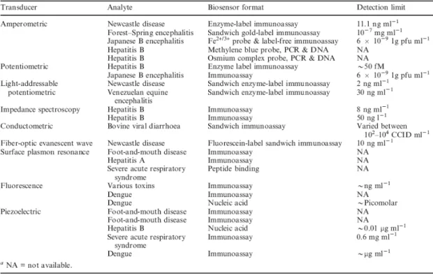
A summary of selected biosensors used for the detection of biomolecules
Chapter 2: Literature Review
Table 2.1 ...36
The characteristics comparison of four kinds of nanowire fabrication
Table 2.2 ...37
The advantages for our fabrication method
Chapter 4: Results and Discussions
Table 4.1 ...59
Device parameters with channel width = 100nm and channel length = 1μm
Table 4.2 ...6968
List of Figures
Chapter 1: Introduction
Figure 1.1 ...4
The semiconductor industry roadmap of memory technologies and the associated lithographic technologies used to manufacture each generation of devices. Each box displays each device generation’s memory size and critical feature size (nm).
Figure 1.2 ...5
The concept of patterning process
Figure 1.3 ...6
The process of nanoimprint method
Figure 1.4 ...9
Process of the soft lithography [5]; (a) formation of an elastic stamp, (b) micro-contact printing, (c) micro-molding in capillaries
Figure 1.5 ...9
Nanoimprint over topographies and multilayer 3D printing
Figure 1.6 ...10
Schematic diagram of a typical biorecognition element
Figure 1.7 ...12
Schematic representation of the principle of electrochemical detection of DNA damage and DNA-damaging agents
Figure 1.8 ...12
Schematic structure of the experimental setup for the detection of IgE using an aptamer-modified FET device integrated with microfluidic system
Figure 1.9 ...14
Typical set-up for a SPR biosensor. Surface plasmon resonance (SPR) detects changes in the refractive index in the immediate vicinity of the surface layer of a sensor chip. The SPR angle shifts when biomolecules bind to the surface and change the mass of the surface layer. This change in resonant angle can be monitored non-invasively in real time as a plot of resonance signal versus time
Figure 1.10 ...16
Schematic illustration of a highly sensitive 27-MHz QCM
Chapter 2: Literature Review
Figure 2.3 ...21
(a) The optical image of the central region of a sensor used for the DNA sensing study. (b) and (c) Representative SEM images showing the SiNW bridging two contact leads
Figure 2.4 ...21
(a) Optical image of the central region of a sensor showing a portion of the lead and the bridged nanowire used for the DNA sensing; (b) schematic drawing of the SiNW with varying widths corresponding to the image in (a); (c) a SEM image showing a 50-nm-wide SiNW, which extends between two contact leads.
Figure 2.5 ...23
SEM image of SiNW after reaction of the GNPs with APTMS
Figure 2.6 ...23
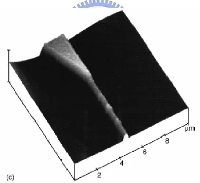
ID-VG curves of SiNW after binding of different molecules on the surface of SiNW. The turn-on voltage was changed after binding of different molecules
Figure 2.7 ...24
The 3-D AFM image of 40 nm width Pt-silicide nanowire
Figure 2.8 ...25
The immobilization steps for the DNA on the Pt-silicide nanowires
Figure 2.9 ...26
Device fabrication and electrical performance. (a) Schematic of active channel. The source, drain, and back-gate are labeled; (b) SEM and (c) OM image of a device; (d) ISD for varying VGD, illustrating p-type behaviour; (e) ISD for VGD for forward and reverse sweep. (f) Hall and drift mobilities versus temperature
Figure 2.10 ...27
Schematic diagram diagram of device. (a) The diagram of the SiNW with side-gate; (b) The nanowire; (c) A SiNW with a Au/Ti side-gate. (d) The SEM image for three SiNW devices on the same chip; (e) An OM image of the flow chamber sealed on top of the devices
Figure 2.11 ...29
NW-FET sensors. (a) Schematic of a p-type FET device. S, source; D, drain; and G, gate electrodes; VG, gate voltage; (b) (left) TEM images of a 20-nm-diam
single-crystal SiNW and (right) an OM image of a device; (c) Schematic of a sensor with antibody receptors (blue); binding of a protein with a net negative charge results in an increase in conductance; (d) NW sensor biochip with integrated microfluidic
Complementary sensing of PSA with p-type (NW1) and n-type (NW2) NW devices; (e) Schematic of array detection of multiple proteins; (f) Detection of PSA, CEA, and mucin-1 with NW1, NW2, and NW3 functionalized with antibodies. Protein solutions of PSA, CEA, and mucin-1 were delivered sequentially to the array. (g) The drop of blood corresponds to the quantity required for analysis. Conductance versus time data recorded for the detection of PSA. NW2 was passivated with ethanolamine
Chapter 3: Experiments
Figure 3.1 ...43
Process flow chart of the side-gated SiNW-FET device fabrication on the SOI wafer.
Figure 3.2 ...44
Comparison of conventional and modified process flow chart of the side-gated SiNW-FET device fabrication using LOCOS process
Figure 3.3……….43
The shrinking nanowire and individual side-gate are achieved by our modified LOCOS process
Figure 3.4 ...46
The process of making PDMS microfluidic channel
Figure 3.5 ...46
The image of syringe pump (model-120) is used in my thesis
Figure 3.6 ...465
The figure of stainless steel clamping apparatus
Figure 3.7 ...476
The real image of PDMS mold, clamping holder and integration of the system.
Figure 3.8 ...476
Schematic structure of the experimental device integrated with microfluidic system and combined with transducer analyzer
Figure 3.9 ...487
Schematic structure of the amplification of the right-hand (nanowire active area) area in figure 3.8 for the detection of antigen using an antibody-modified FET device integrated with microfluidic system
Figure 3.12 ...510
The schematic process of detecting FAM-labeled target-DNA hybridizes with the side-gated SiNW-FET by fluorescence assay
Figure 3.13 ...53
The schematic process of detecting anti-alpha-fetoprotein and AFP onto the side-gated SiNW-FET
Chapter 4: Results and Discussions
Figure 4.1 ...56 (a) Top-view layout of a side-gated SiNW-FET. (b) Amplification of the left-hand
area in (a). (c) Amplification of the area dotted in (b)
Figure 4.2-1...57
SEM images of side-gated SiNW-FET with channel length = 1μm
Figure 4.2-2...57
SEM images of side-gated SiNW-FET with channel width =100 nm
Figure 4.3-1...58
The ID-VG characteristic of the SiNW-FET
Figure 4.3-2...58
The ID-VD characteristic of the side-gated SiNW-FET
Figure 4.4 ...62
The real-time versus ID detection curve acquired from alkaline (pH=9) solution
Figure 4.5 ...62
The real-time versus drain-current detection curve acquired from acidic (pH=4) solution
Figure 4.6 ...63
The real-time versus drain-current detection curve acquired from alkaline (pH=9) to acidic (pH=4) solution
Figure 4.7 ...63
The ID-VG curve of alkaline (pH=9) solution and acidic (pH=4) solution detection.
Figure 4.8 ...64
SiNW-FET for pH detection. Schematic illustrating the SiNW nanosensors for pH sensing. Zoom of the APTES-modified SiNW surface illustrating changes in the surface charge state with pH value
Figure 4.10 ...676
The mechanism of the SiNW-FET for detection of biomolecules
Figure 4.11 ...687
The noise level of HEPES+EDTA solution during different temperatures measured by UV spectrophotometer
Figure 4.12 ...687
The noise level of PBS solution during different temperatures measured by UV spectrophotometer
Figure 4.13 ...70
Noise of SiNW-FET device in real-time detecting by HP-4156C analyzer
Figure 4.14 ...68
Real-time detection of the target-DNA hybridizing with probe-DNA at 20°C.
(Plot of drain-current versus time for modified SiNWs, where region 1 corresponds to stabilize device, region 2 corresponds to the buffer solution, region 3 corresponds to the addition of 100fM target-DNA, region 4 corresponds to addition of 100pM target-DNA and region 5 corresponds to addition of 10nM target-DNA)
Figure 4.15 ...71 The ID-VG curve of detection for DNA hybridization assay at 25oC
Figure 4.16 ...73
The ID-VG curve of the detection for DNA hybridization assay
Figure 4.17 ...74
The Hyperchromic-Effect in DNA hybridization assay
Figure 4.18 ...75
The record of OD260-curve during DNA hybridization assay with variation temperature continuously
Figure 4.19 ...75
The record of OD260-curve during DNA hybridization assay with variation temperature continuously
Figure 4.20 ...776
The fluorescent images under treated different hybridization experimental conditions with the same oxide substrate
Figure 4.24 ...79
Real-time detection of target-DNA hybridizing with probe-DNA ranging from 60 to 20 °C. (Plot of ID versus time for modified SiNWs, where region 1 corresponds to stabilize device, region 2 corresponds to the buffer solution, region 3 corresponds to the addition of 100 fM target-DNA, region 4 corresponds to addition of 100 pM target-DNA and region 5 corresponds to addition of 10 nM DNA
Figure 4.25 ...80
The ID-VG curve of detection for hybridization assay ranging from 60 to 20 °C
Figure 4.26 ...82
Characteristic of the DNA sensor measured in PBS buffer solution containing target-DNA, VD=0.5V. It shows theΔID positive related to logarithmic scale of target-DNA concentration
Figure 4.27 ...84
Absorption spectrum of the antibody of AFP heterostructure between 4000 to 500 cm-l
Figure 4.28 ...84
Absorption spectrum of the antibody of AFP heterostructure between 2000 to 400 cm-l
Figure 4.29 ...86
Real-time detection of AFP interaction with anti-AFP. (Plot of ID versus time for modified SiNWs, where region 1: stabilize device, region 2: the buffer solution, region 3 to region 7: addition of different concentration from 3ng/mL to 600ng/mL AFP and region 8: injection with hot-water flow out)
Figure 4.30 ...88
The ID-VG curve of detection for AFP interaction with antibody and denaturation assay
Figure 4.31 ...88
Real-time detection of BSA protein. (Plot of ID versus time for blocking modified SiNWs, where region 1: stabilized device, region 2: addition the PBS solution, region 3: injection the solution including the BSA solution
Figure 4.32 ...890
Characteristic curve of the AFP sensor measured in PBS buffer solution containing antigen-AFP. Drain voltage was set at +0.5V. It shows theΔID positive related to
Chapter 1: Introduction
1.1 General Introduction
Nanotechnology has become a very popular word that is used to describe many types of research in which the characteristic dimensions are below 1000 nm. For example, continuing improvements in lithography have resulted in the reduction of line widths to well below 1 micron. This kind of work is often called nanotechnology. The interdisciplinary study of biology, chemistry, and electronics became more and more important than ever before. Combining biotechnology and semiconductor technology, various types of biochips and biosensors have now been developed to detect the specific binding of biomolecules on the solid-state substrates. As semiconductor devices become scaled down to ever-smaller sizes within the nano-regime, a variety of technological and economic problems arise, the rules of classical physics give way to quantum mechanics, and the term “molecular-scale” becomes more accurate than “nano-scale.” At this point, the scaling of sizes that has successfully reduced device features from the micro-scale to the nano-scale reaches its limits, and, therefore, alternative manufacturing methods, materials, device structures, and architectures are required. In this regime, the approach of fabricating nanoelectronic devices and interconnects using a combination of molecular and nanostructured materials with existing and emerging processing technologies promises to allow the continued miniaturization and enhancement in performance of the biotechnology. Nanotechnology is a revolution in science and technology. It distinguishes itself from all previous scientific and industrial revolutions in many
strategy and the ‘‘top-down’’ approach [1]. The pros and cons of the ‘‘bottom-up’’ and ‘‘top-down’’ approaches to nanotechnology are matters of hot debate in the most reports. It is widely held that the present top-down semiconductor technology has not exploited the physics and chemistry of nano-materials on the one hand, and not taking advantage of the development of bottom-up nanotechnology on the other. Many reasons come to mind. Firstly, nanomaterials and their properties in the nanorealm, especially at the interface, are not well understood and still under investigation. Secondly, the fabrication techniques, both at the materials level and at the device stage, are not well defined or fully developed. Thirdly, connection to the macro world remains a real problem. Finally, even if all these problems can be overcome, they are at present not mass producible and cost competitive enough to challenge the existing semiconductor technology. For a stand-alone bottom up nano-device to challenge the top-down nano-device, it must overcome these hurdles and integrate into it. While each approach has its advantages and disadvantages, it is our view that future development of nanotechnology will probably encompass both approaches with their relative contributions depending upon specific applications. In this thesis, we discuss the top-down nanotechnology firstly, followed by the recent developments in biosensors, and finally talked about the importance of detecting biomolecules. While this seems to be a reasonable road to fabricate novel nano-devices, ultimately though, nano-devices will be replaced by traditional molecular, atomic, and nuclear devices, as the size further diminishes, as we shall discuss later in this thesis.
1.2 Introduction to Top-Down Nanotechnology
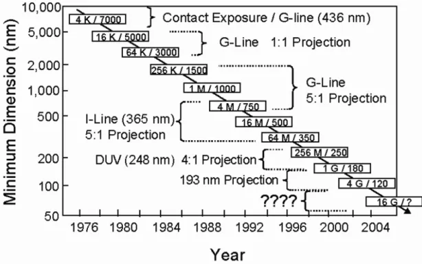
“Top-down” methods start with patterns made on a large scale and reduce its lateral dimensions before forming nanostructures. This approach seeks to fabricate nanodevices on silicon chips directly using electron beam or X-ray lithography (either photolithography or electron lithography) [2]. Indeed, the top-down approach has been the method of choice in the semiconductor industry for making microelectronic and other devices for decades. The semiconductor industry entered the nanotechnology era in the year 2000, and by 2004, the industry was shipping devices with physical gate dimension of less than 40 nm and insulator thickness of less than 1 nm. This is in line with the pace of Moore’s Law [3]. The current development of the optical lithography at 193 nm wavelength is pushing the limit of 32 nm (half pitch). Dimensions smaller than 32 nm is generally viewed as beyond the capabilities of optical lithography at 193 nm wavelength, unless high-index fluids, high-index lens materials, and higher-index resist can be developed is shown in figure 1.1. Another way to extend the lifetime of optical projection lithography with immersion to 32 nm half pitch and beyond is to divide the pattern into two or more masks. It is generally believed that extension of the Roadmap for semiconductor industry beyond 32 nm will probably require the development of ‘‘next-generation’’ lithography (NGL) technologies such as extreme ultraviolet lithography (EUVL), mask-less (ML2), and imprint lithography.
Figure 1.1 The semiconductor industry roadmap of memory technologies and the
associated lithographic technologies used to manufacture each generation of devices. Each box displays each device generation’s memory size and critical feature size (nm).
A beam of light passes through the mask and a lens, which focuses an image on photoresist placed on a surface of a silicon wafer or a film in figure 1.2. The resolution of the photolithographic process determines the width of the channels. In photolithography ultraviolet light is used. The fabrication of spacing smaller than half this length causes blurred features, which can melt together. Various technical improvements managed to reach structural resolutions in the order of 70 nm in experimental setups and about 100 nm in mass production [4, 5]. The technical
technologies based on focused beams are used electron-beam lithography (EBL) and focused-ion beam (FIB) lithography to create nano-channels, e.g., for DNA separation
[6]. Features of 10 nm in scale can be achieved by top-down methods. Fabricating the
high-performance integrated circuits requires increasingly shorter wavelengths of the radiation source to manufacture devices of decreasing critical sizes.
Figure 1.2 The concept of patterning process
Above mentioned have been introduced for the fabrication of electronic devices. Maybe other approaches are all potential “next-generation lithography” (NGL) technologies, but currently they remain expensive and difficult to operate and implement. Because the ‘‘next-generation’’ lithographies will most likely require the development of substantially new infrastructure, implementation of these new technologies as viable manufacturing solutions can be a real challenge for the industry
have high reflectivity at 13.5 nm wavelength. For definitions or features finer than 32 nm, it is necessary to use electron beams or X-rays in the so-called ‘‘nanoimprint lithography (NIL) ’’ displayed in figure 1.3 [8–10]. High-energy electron beams or X-rays can provide definitions of a few nanometers. The current definition in NIL using electron beams is about 5 nm [8–10]. It is obvious that nanoimprint lithography can achieve much better resolution than EUVL discussed earlier. However, it suffers from, among other things, cost effectiveness, mass production capability, and defect tolerance problems. The main reason for this is that NIL is essentially a multilayer mold technology. It is interesting to note that, at or below about 15 nm, quantum confinement sets in, making single-nanowire devices a reality. Indeed, 15 nm wide SiNW channel and 5–10 nm isolated silicon islands were used in the work of Tsutsumi et al. [11]. This is a fast-developing technology [13–28].
And then, figure 1.4 presents the concept of soft lithography [5],which is based on the use of elastomeric polymers to transfer a pattern from a master to a large number of copies having single-layer structures to define the nano-size pattern. Furthermore, soft lithography has great potential because it does not require expensive equipment or a high-quality clean room, but it is ineffective for fabricating multi-layer structures or for allowing precision alignment. In soft lithography in figure 1.4(a) the mold is usually made by producing a pattern in a layer of photoresist on the surface by photolithography or electron-beam lithography (EBL) [1]. Then a liquid precursor poly-dimethyl-siloxane (PDMS) is poured over it and cured into the rubbery solid. The PDMS stamp is then peeled off the master. Copying the pattern on the PDMS stamp as well as the use of the stamp is, however, cheap and easy. The PDMS stamp is then further used in different ways to make nanostructures: by micro-contact printing [12] in figure 1.4(b) or micro-molding in capillaries [6] in figure 1.4(c). The advantage of the soft lithography is that it does not need to be carried out in the clean room. The nanostructures made by this method can be produced in a wide range of materials and the patterns can be formed on curved and planar surfaces. However, this technique is not suitable for complex nano-electronic devices, i.e., for making multilayered structures due to the deformations and distortions of the soft PDMS stamp that can cause small errors in the replicated pattern and the misalignment of the pattern. The latter limitation can be overcome by employing a rigid stamp in step-and-flash imprint lithography [13, 14] and nanoimprint lithography (NIL) [15,
large-scale and nanoscale patterns simultaneously [17]. The key to successful nanoimprint is preventing residual mold attachment after it is removed from the resist coating substrate during the imprinting process.
The pros and cons of the top-down approaches to nanotechnology are discussed. While this approach has its advantages and disadvantages, it is our view that future development of nanotechnology will probably embrace both approaches with their relative contributions depending upon specific applications (e.g. performance enhancement, materials improvement, functionalization, etc.) [18].
Figure 1.4 Process of the Soft lithography [5]; (a) formation of an elastic stamp, (b)
1.3 Introduction to Biosensor
Generally, biosensors are distinguished from one another by the nature of the process and according to their biochemical or biological component, e.g., biocatalytic, immunological molecules and nucleic acid. The transducer is the other component of the biosensor shown in figure 1.6, which also plays an important role in terms of converting the bio-recognition event into an electrical signal or other different kind of signal output. The transducers employed for detection include electrochemical, optical, and piezoelectric platforms. The detection strategies of the transducers can be divided into two categories, that is, labeled and label-free. The former relies on the detection of a specific label signal, and the latter is direct measurement of a signal occurring during the biochemical reactions on a transducer surface. The label-free method is more attractive than labeled because the extra label process is unnecessary, and hence research about label-free biosensors continues to grow [19, 20]. The biosensors are more common and extremely successful in most of platforms and presenting a selection of the most significant technologies and advances in relation to biological monitoring.
1.3.1 Electrochemical biosensors
More than half of the biosensors used for the detection of biomolecules are based on electrochemical transducers [21]. A large amount of reports have demonstrated the importance of the electrochemical biosensors in the field of clinical and environmental analysis [21, 22]. The electrochemical biosensors have many advantages, such as low cost, high sensitivity, independence from solution turbidity, easily miniaturized and well suited to micro-fabrication, low power requirements, and relatively simple instrumentation [23]. These characteristics make electrochemical detection methods highly attractive for field monitoring of biological agents. The method used in many cases depends on the type of change along with the properties of the analyte and matrix. A discussion of the electron transfer mechanisms that commonly occur with amperometric-based biosensors are shown in figure 1.7.
Despite the features of remarkable sensitivity, rapid response, miniaturization capability, and low cost, the electrochemical biosensors still have problems with long-term stability and selectivity in blood sample. Obviously, further work would be required to demonstrate that the electrochemical biosensors do suffer from biofouling problems. Such problems can be partly addressed by covering the transducer or sensor surface with an appropriate microfluidic system shown in figure 1.8. Notwithstanding, the use of disposable screen printed electrodes appears to be a realistic strategy for target biomolecules detection. Consequently, screen printed electrodes have attracted much attention recently as a platform in DNA, immunoassay and enzyme-based biosensors [24, 25]. About this strategy may be somewhat limited to applications that
Figure 1.7 Schematic representation of the principle of electrochemical detection of
1.3.2 Optical biosensors
When a light illuminates onto a sample, a lot of information can be manifested by either reflection or transmission. This phenomenon depends on the wavelength of light, the angle of incidence, the sample composition and sample thickness. By exploiting the energy from the electromagnetic spectrum, it can be used to provide information about the changes in the local environment surrounding the analyte. Optical biosensors, which sometimes referred to considerable interest on the detection of biomolecules [26].Therefore, biosensors based on surface plasmon resonance and fluorescence principles are the most common and promising methods for target molecules detection. Recent reports about related technologies suggest that optical biosensors possibly become a powerful tool in the future for the real-time and biomolecular detections [27]. Figure 1.9 shows the surface plasmon resonance (SPR) being a form of reflectance spectroscopy that has been widely used in biosensor development. It has been demonstrated that SPR plays a significant role in relation to immunogenicity, proteomics, drug discovery, and DNA analysis [28]. This method is particularly attractive for direct and label-free detection and many previous works have shown that the SPR-based biosensor is also a tool for target molecules monitoring. SPR is one of very few techniques that are able to provide non-invasive, real-time kinetic data on association and dissociation rates, along with equilibrium binding constants for receptor systems. Although SPR is an interesting and appealing transduction method, the measuring is limited to a very small range. There seems to be developed a hand-held SPR device that can be used to detect biomolecules directly.
sample such as blood and serum. If these devices are used for the detection of biomolecules routinely, one of the challenges limits the application of SPR for real-time measurement in blood is that the signal is very sensitive to non-specific physical binding on the surface [21]. Notwithstanding, the capability to perform real-time measurement is an area of significant interest for the detection of target molecules [29].
Figure 1.9 Typical setups for an SPR biosensor. Surface plasmon resonance (SPR)
detects changes in the refractive index in the immediate vicinity of the surface layer of a sensor chip. The SPR angle shifts when biomolecules bind to the surface and change the mass of the surface layer. This change in resonant angle can be monitored non-invasively in real time as a plot of resonance signal versus time.
1.3.3 Piezoelectric biosensors
Piezoelectric biosensor works on the principle that the frequency variation of an oscillating quartz crystal correspond to changes in mass as a result of a biochemical reaction and bio-recognition event [30], as shown in figure 1.10. One of the piezoelectric sensors is quartz crystal microbalance (QCM), which has been used to detect target molecules [30]. It has been evaluated the detection limit of various biosensor platforms and concluded that the piezoelectric method is inferior compared to electrochemical and optical detectors [30]. Notwithstanding, some studies about detection of biomolecules by using the piezoelectric sensor approach increased recently. It was demonstrated that the molecular imprinting technique may be a promising method for solving problems from non-specific interactions. The QCM transduction method is an attractive option for real-time monitoring of target molecules.
Despite the promising analytical performance of the piezoelectric sensor further work still needs to be undertaken to evaluate the stability of the sensor surface in biological fluids. Problems such as crystal regeneration, relatively long incubation times, nonspecific binding of proteins or other biomaterials, and loss of material coating after washing are well known limitations of this technique, [22, 30] which still require further attention before this biosensor technology platform is used routinely for target molecules detection.
1.4 Introduction to the Importance in Detection of Biomolecules
A number of biosensors have been developed to detected important biomolecules. However, all of them essentially comprise a biological recognition element or bio-receptor, which interacts with the analyte and responds in some manner that can be detected by a transducer, as shown in figure 1.6. The biological recognition element is a crucial component, and its function is to impart selectivity so that the sensor responds only to a particular analyte of interest, hence avoiding interferences from other substances. Table 1.1 summarizes the main analytical features of a wide range of biosensors, noting that a majority of the existing technologies used for detecting target molecules rely on antibodies as the recognition molecule [5]. Antibodies are the critical part of an immuno-sensor, since their quality contributes to the sensitivity and specificity [5].
It is important to note that the success of an immuno-sensor depends heavily on which antibodies, labels, and reagents are used in the assay. Once antibodies of the desired specificity and affinity have been developed, they can be incorporated in a wide range of transducer platforms. DNA is an alternative recognition molecule that has also received some attention for the detection of target molecules. A large number of excellent papers have been reported based on nucleic acid hybridization. And noting that the detection of specific DNA sequences provide the fundamental basis for monitoring a wide variety of genetic diseases and viral infections [11-16]. Despite of the great deal of work in this field, the application of a DNA biosensor for target molecules detection is still in its infancy. One of the major requirements in developing a biosensor for target molecules is the need of a sensitive analytical device that can not only achieve low detection limitation easily but also high selectivity. Many infectious diseases will spread rapidly through a community before any symptoms are identified. If a biosensor can detect low levels of antigen easily at the onset of infection will be invaluable. In addition, a biosensor that is relatively cheap, robust, responds rapidly and provides high-throughput is highly desired for applications. However, the type of biosensor used for target molecules will in many cases depend on the properties of the analyte (i.e., size, structure, concentration, etc.) and the matrix (i.e., air, liquid). The most commonly used bio-sensing methodologies for detecting two important biomolecules will be described in detail in next chapter.
Chapter 2: Literature Review
2.1 Silicon Nanowire Field Effect Transisitor (Top–Down SiNW-FET)
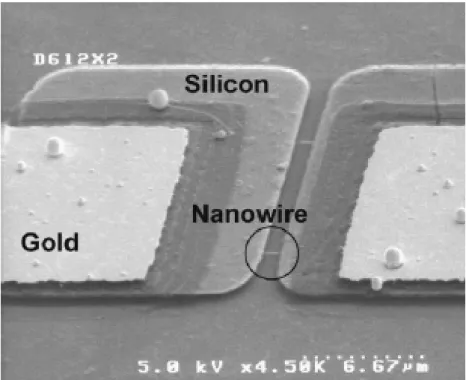
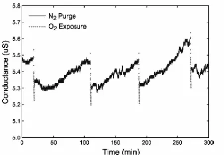
Bashir and co-workers [1] described SiNW-FET sensor process that was realized using the “top–down” microelectronics processing techniques. A process known as confined was utilized to obtain single crystal silicon nano-plates that are thin as 7nm and nanowires small as 40nm in diameter at precise locations, as shown in figure 2.1 [2]. The method allowed the realization of truly integrated dense array of sensor. Initial testing of the device showed that sensitivity towards oxygen ambient, and suggested it possibility of using these sensors for chemical and biological detection shown in figure 2.2 [1].
Figure 2.1 Field emission scanning electron microscopy photos of the fabricated
Figure 2.2 Electrical response of the device upon exposure to oxygen and nitrogen.
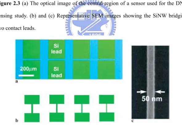
Li et al. [3, 4] fabricated a single crystal silicon nanowire with 50 nm width on SOI wafer by electron bean lithography. They have demonstrated the detection of DNA molecules based on their intrinsic charge by using SiNWs fabricated by top-down semiconductor processes. This method created a pathway for fabricating high-density, high-quality, and well organized nano-scale sensor that can be integrated with communication circuits, as shown in figure 2.3 [3]. Sequence-specific and label-free DNA sensors based on SiNW with probe-DNA or PNA molecules covalently immobilized on the surfaces in figure 2.4 [4]. Label-free DNA was recognized when the target DNA was complementary with the probe-DNA attached onto the SiNW surfaces, causes the change to accumulate on the surface of the SiNW. But there are two disadvantages blocking the development of this device. One was they use high cost substrate-SOI wafer, the other one was the device lack of individual
Figure 2.3 (a) The optical image of the central region of a sensor used for the DNA
sensing study. (b) and (c) Representative SEM images showing the SiNW bridging two contact leads.
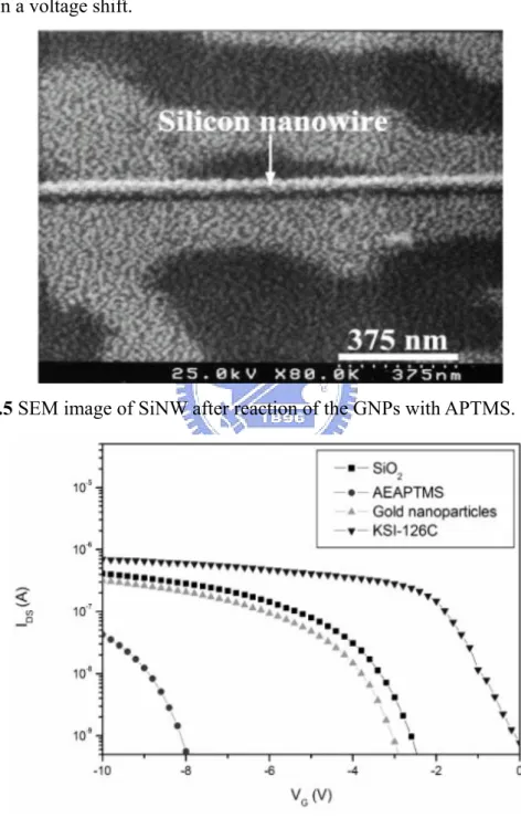
Sheu et al. [5] demonstrated the bio-detection by using the SiNW whose surface was pretreated by APTMS and then selectively deposited with gold nanoparticles, as shown in figure 2.5 and figure 2.6 [5]. The GNPs on the surface served as linkers for detection. The target molecules bound with GNPs on the surface of the SiNW and resulted in a voltage shift.
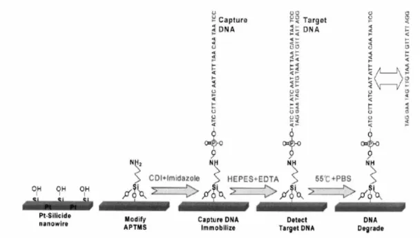
Ko et al. [6] developed a self-aligned platinum-silicide nanowire for biomolecules sensing was shown in figure 2.7. The immobilization steps of the DNA onto the nanowire are illustrated in figure 2.8 [6]. The 40 nm-width nanowire is fabricated through a sequence of electron-beam writing on the poly-Si film, line shrinking by alkaline solution, platinum film depositing, 550°C annealing, and aqua dissolution is performed. The immobilization of capture-DNA on the platinum-silicide nanowire is verified from the fluorescence-labeled technique. The FET can distinguish the complementary, mismatched, and dehybridized DNA via the conductance difference. They can sense the minimal target DNA concentration down to 100fM. Unfortunately, this SiNW-FET device cannot integrate with microfluidic system to detect real-time response.
Figure 2.8 The immobilization steps for the DNA on the Pt-silicide nanowires.
Eric Stern et al. [7] have demonstrated an approach to realize the characteristic of the SiNW sensors for specific label-free antibody detection. The images and electrical properties of the SiNW sensors are shown in figure 2.9. This approach has potential for extending single device to an integrated system, with widely use as the chip-arrays. However, ‘top-down’ fabrication produced successful solution-phase nanowire sensing has been demonstrated for proteins [5, 6], and DNA [7, 8, 9, 10]. Here they reported the uses of CMOS-FET compatible technology and hence demonstrate the specific label-free detection of concentrations of antibodies as well as real-time monitoring of the response. But this kind of device is without independent controlling back-gate.
Figure 2.9 Device fabrication and electrical performance. (a) Schematic of active
channel. The source, drain, and back-gate are labeled; (b) SEM and (c) OM image of a device; (d) ISD for varying VGD, illustrating p-type behaviour; (e) ISD for VGD for forward and reverse sweep. (f) Hall and drift mobilities versus temperature.
Pritiraj Mohanty et al. [11] demonstrated the fabrication, functionalization, and operation ofa nano-electronic FET for pH sensor, as shown in figure2.10. The SiNW with side-gate is fabricated with standard semiconductor process.The functionalized SiNW can be controlled with local side-gate to induce inversion or depletion layers. This approach offers the possibility of highly parallel detection of ion orcharged protein and DNA with control of individual elements. By selective gate-voltage, individual NWs in an array can beturned on or off during sensing process. Therefore, the array contains multiple receptors for the detection of multiple chemical and biological species in a single integrated chip. But this SiNW device is without oxide acting as dielectric layer to level down the field effect characterization. Also their fabrication starts from the high cost SOI wafer.
2.2 Real-time Nanowire Field-Effect-Transisitor Biosensors
Detectors based on semiconductor NWs are configured as FETs, which exhibit a conductivity-relevance change in response to variations in the electric field or potential at the surface [8]. The dependence of the conductance on gate voltage makes FET natural candidates for electrically based sensing, because the electric field effect resulting from the binding of a charged species is the effect of applying a voltage with a gate electrode. They can be prepared as p- or n-type materials and configured as FET in figure 2.11(b) that exhibits better electrical characteristics achieved for silicon devices [12, 13, 14]. The superior switching characteristics of SiNWs are important factor that achieve excellent sensitivity. The binding of biomolecules onto the surface of the NW leads to depletion or accumulation of carriers in the nanometer-diameter structure, versus only the surface region of a device. This semiconductor NWs provides sufficient sensitivity to enable the detection of important biomolecules in solution. However, because these are field-effect devices, detection sensitivity depends on the ionic strength of the solution. A sensing device can be configured from high-performance NW-FET by linking NW receptor groups that recognize specific molecules to the surface of the NW in figure 2.11(c). When the sensor device with surface receptors is exposed to a solution containing biomolecules, such as protein that has a net negative charges in the aqueous solution, specific binding will lead to an increase in the surface and in conductance for a p-type NW device. As a proof of concept, there are some reports have developed a microfluidic system integrated NW sensor that incorporates SiNW with well-defined p- or n-type doping;
fluid-based assembly of NWs to align them and spacing over large areas. Photolithography and metal deposition define interconnections to a large number of individual NWs in parallel array in figure 2.12 [15].
Figure 2.11 NW-FET sensors. (a) Schematic of a p-type FET device. S, source; D,
drain; and G, gate electrodes; VG, gate voltage; (b) (left) TEM images of a 20-nm-diam single-crystal SiNW and (right) an OM image of a device; (c) Schematic of a sensor with antibody receptors (blue); binding of a protein with a net negative
Figure 2.12 NW arrays for multiplexed protein sensing. (a) Illustration of NW array
fabrication; (b) Optical image of a NW array; (c) Data recorded from p-SiNW devices; NW1 was immobilized with PSA-Ab1, and NW2 was modified with ethanolamine; (d) Complementary sensing of PSA with p-type (NW1) and n-type (NW2) NW devices; (e) Schematic of array detection of multiple proteins; (f) Detection of PSA, CEA, and
Recently, the biosensor has employed increasingly in a variety of applications where continuous measurements in biological media are required by real-time monitoring sensing [16]. A biosensor is distinguished from a chemical sensor in that it possesses a biological recognition element, typically a protein, peptide or oligonucleotide. The goal in this subject may measure the rate of uptake or efflux of relevant species or to establish spatial distributions in real-time sensing [17]. When a sensor is brought in contact with biological tissues, sensor performance can deteriorate. The exact causes of this deterioration are not clear, but are a mix of passive adsorption of biomolecules on the sensor probe surface and active processes coupled to tissue response [17]. For this reason, we will give some attention to approve the microfluidic system that can play key roles in regulation of detection events. This affords a greater range of analytical approaches to analysis, including separations and derivatization not possible with a single real-time sensor array.
2.3 Detection of Important Cancer Markers 2.3.1 Introduction of Mutation Genes-BRAFV599E
Cancers arise owing to the accumulation of mutations in critical genes that alter normal program of cell proliferation, differentiation and death [18]. Recently, a somatic point mutation in the BRAFV599E
gene has been identified as the most
common genetic event in papillary thyroid carcinoma [19]. In a series of 78 papillary carcinomas, 36% of tumors harbored a thymine-to-adenine transversion at nucleotide position 1796, which results in a valine-to-glutamate substitution at residue 599
carcinomas, the most frequently affects the hot spot in other types of human cancers where BRAFV599E
is mutated, such as malignant melanoma and colorectal carcinoma
[21, 22]. The initial reports indicated that BRAFV599E
mutations in thyroid tumors are
restricted to papillary carcinoma, because no mutation was observed in other types of well-differentiated thyroid cancer [20, 21]. However, it remains unclear whether this gene is also mutated in poorly differentiated and anaplastic thyroid carcinomas, which are the most aggressive types of thyroid neoplasm. In addition, it is important to determine whether BRAFV599E
mutation confers papillary carcinomas with distinct
phenotypical and biological properties. In this study, they analyzed a series of 320 thyroid tumors and benign nodules for BRAFV599E mutation, report a novel method of screening for the mutation, and provide a detailed comparison of clinical-pathologic features between thyroid tumors according to their BRAFV599E
status. The high
prevalence of BRAFV599E mutations in papillary carcinomas and the specificity of this alteration to papillary carcinomas or less differentiated tumors developing from papillary carcinoma make it a potentially important marker for tumor diagnosis and prognosis in future real-time biosensors. Testing for BRAFV599E
mutations in thyroid
tumors is simplified by the fact that virtually all of them are restricted to the nucleotide position 1796. This relatively simple, quick, and sensitive method can be used not only in tissues harvested at the time of surgery but also for the preoperative diagnosis of thyroid specimens. In addition, BRAFV599E may be a valuable target for cancer marker currently being developed to diagnose its activity. This would be of a particular importance for carcinomas that represent a major source to detect the
2.3.2 Introduction of Cancer Marker Alpha-Fetoprotein
Hepatoblastoma (HB) is the most common primary liver tumor of childhood but accounts for less than 1% of all paediatric tumors [23]. Hepatocellular carcinoma (HCC) is one of the most common causes of cancer-related deaths in Asia, especially in Taiwan [24]. The main treatment for HCC is surgical resection, but less than 15 % of patients can benefit from this treatment due to the presence of multi-focal tumors and the risk of post-operative hepatocellular deficiency [25]. The introduction of cisplatin into treatment in the early 1980s dramatically improved the prognosis for most children with HB and survival rates have risen to at least 70% in most recent large series [26, 27]. The prognosis mainly depends on disease extension at the time of diagnosis and the completeness of surgical resection. However, the level of serum alpha-fetoprotein (AFP) at diagnosis has also been shown to impact the outcome [28,
29]. Alpha-fetoprotein, a glycoprotein with an electrophoretic mobility of 1-globulin,
is produced in the fetal yolk sac, liver and intestine [30]. After birth, production of AFP is almost totally repressed, but it reappears and is over-expressed in about 60 to 70% of patients with HCC, which makes it a useful biomolecule marker in the diagnosis of this malignancy and liver cancer [31]. Von Schweinitz et al. were the first team to point out that it would be a negative prognostic factor in suffering from HB when the concentration of serum AFP level was below 30ng/mL [24, 28]. This finding resulted in an protocol recommending that future patients with HB and a standard level of AFP at diagnosis should be categorized as high-risk regardless to the extent of the disease at diagnosis, and should be treated with more aggressive
nonetheless exhibit some common characteristics such as widespread disease at presentation, chemoresistance and a poor outcome, which signal intrinsically aggressive genetic and biological tumor profiles. Clearly, more investigations and large-scale cooperation among groups involved in HB research are warranted to further improve well-known understanding of these heterogeneous tumors.
Clinical experience and in vitro studies demonstrated that the levels of AFP may vary in patients with HCC. In addition, tumor recurrence rates are rather high in patients with HCC who received surgical treatment. Therefore, novel detection strategy for liver cancer has been investigated. In the current study, we focused on refining the component of tumor receptor-mediated adenoviral vector retargeting using currently varieties of biosensors.
2.4 Motivation
Ultra-sensitive detection of biomolecules is fundamental to the detection of biomolecular analysis. 1-D nanostructures have been demonstrated as good candidates for ultra-sensitive, label-free, miniaturized molecule sensors in the applications. Among the “top-down” systems explored and comparison with previously reported methods is given in Table 2.1, the sensors based on SiNW, could be understood in terms of change of surface charge with the presence of molecular species. However, here we demonstrate the detection of important biomolecules based on their charge by using SiNW fabricated by “top-down” processes. This method created a way to fabricate high-density and high-quality biosensor that can be integrated with the following advantages listed in Table 2.2. To solve the back-gate problem, the structure of side-gate is configurated in my thesis, addressing all devices on the wafer were the gate be addressed individually of NW-FET. The shrank nanowires with higher surface-to-volume ratio and individual side-gate for integration are achieved by the LOCOS process. The detection sensitivity is therefore greatly enhanced as the signal can be effectively transduced. Our side-gate devices using SOI wafers provide a good quality of gate-dielectric and therefore the electric field was induced effectively by the charged molecule, and the detection signal varied more sensitive. Recently papers have reported about the biological molecules sensing applications, and developed novel real-time biosensors. With the testing sample needs being preceded in an aqueous solution, it usually needs a microfluidic system to carry out. For these reasons, we investigate the process to build the microfluidic system
Table 2.1 The characteristics comparison of four kinds of nanowire fabrication Approach Nanowire with
back-gate (Top-down) Nanowire with back-gate (Top-down) Nanowire with side-gate (Top-down) Nanowire with side-gate (Top-down) Journal Nano Letters
2004 Nature 2007 APL 2006 Biosensors and Bioelectronics 2007
Author Z. Li …etc Eric Stern…etc Pritiraj…etc G.S. Wilson…etc Sensitivity 25pM ≤ 100fM Not mentioned 100fM
Integration Easy (E-beam) Easy (E-beam) Easy (E-beam) Easy (E-beam) Advantages 1. Sensitive 2. Label-Free 3. Sensing array density 4. Real-time detecting 1. Sensitive 2. Label-Free 3. Real-time detecting 1. Sensitive 2. Label-Free 3. Side-gate for integration 4. Making better Ohmic contact 5. Flow-chamber design for faster throughput 1. Sensitive 2. Label-Free 3. Real-time detecting 4. Isolated side-gate for integration 5. Shrinkage Nanowire 6. Good Ohmic contact
Table 2.2 The advantages in our fabrication method
1. Allows for individually nanowire to be within a single microfluidic channel 2 Real-time, label-free, direct-detection of important biomolecules
3 High sensitivity & exquisite selectivity 4. Isolated side-gate for integration process 5. Shrinking-effect of LOCOS process 6. Have potential to be a portable device
7. Fabricate single-crystal NW with SOI wafer with high mobility & sensitivity 8. Eliminating expensive labeling steps and simplifying the signal read-out 9. SOI wafer exhibits lower leakage current and excellent field-effect properties
2.5 Organization of the Thesis
In this thesis, we reported a novel side-gated silicon nanowire field-effect transistor (SiNW-FET) as the cancer marker sensor. We fabricated SiNW on silicon-on-insulator (SOI) wafer with high sensitivity and high detection limitation. Label-free and single-strand DNA and cancer marker anti-AFP were modified onto the SiNW. In order to overcome some challenges in this work, for example, pattern definition, nanowire shrinking, label-free DNA and Anti-AFP modification, microfluidic system integrated with the SiNW and electrical signal detection…etc. In Chapter 1, the general overview of the top-down approach of nanotechnology was introduced. There is an overview discussion with varieties of biosensors for detecting significant bio-molecules ex: cancer markers. Literature reviews reported some “top-down” SiNW-FET biosensors and the fabrication of microfluidic system with device and major motivation of this study are introduced in Chapter 2. The details of fabrication processes, biomolecules immobilized procedures and characterization of detection analysis instruments are presented in Chapter 3. In Chapter 4, the electrical property of side-gated SiNW-FET and the application of DNA and protein markers detection were also discussed. Finally, the summary of important achievements and contributions of this thesis are addressed in the Chapter 5.
Chapter 3: Experiments
3.1 General introduction
Side-gate nanowire field-effect-transistor (NWFET) by electron beam lithography and shrank SiNW by LOCOS process was fabricated. In the fabrication process, all the experiments were proceeded in National Chiao Tung University (NCTU) or National Nano Device Laboratories (NDL) [1]. All the reagents and solvents were of reagent-grade quality, and listed alphabetically in the form of “Name {abbreviation; chemical formula; purity; manufacturer}”. Some information will be omitted if not available or not necessary. The experimental reagents were shown in the following text and used the abbreviation of the reagent.
1. (3-Aminopropyl)triethoxysilane (APTES; molecular formula H2N(CH2)3Si(OCH2CH3)3; purity 98%; Fluka)
The purpose of APTES molecule is to modify the exposed SiO2 surface on silicon nanowire. Ethoxy groups of APTES forms covalent bonding with hydrophilic hydroxyl groups attached to the SiO2 surface to form molecular layer of amino groups in order to bond with biomolecules, ex: DNA and protein.
2.Acetone (molecular formula CH3COCH3; purity 99.5%; Sigma)
Acetone was mixed with Ethanol to clean the surface of wafer.
3. Anti-alpha-fetoprotein (human, AFP) from Mouse monoclonal antibody 4. Antigen of Alpha-fetoprotein (human, AFP) from Mouse monoclonal antigen 5. Deionized and distilled water (DI water, ddH2O)
6. Deoxyribonucleic acids (OPC grade; MDBio Inc.) Sequence Name Oligonucloetide Sequence
Capture DNA 5'-AAATATATTA-TTACTCTTGA-GGTCTCTGTG-3' Complementary Target-DNA 5'CACAGAGACC-TCAAGAGTAA-TAATATATTT-3' Non-complementary target-DNA 5'CACAGAGACC-GCCGTAGTAA-TAATATATTT-3'
7. Ethanol (molecular formula CH3COCH3; purity 99.5%; Sigma)
Ethanol will diluted APTES to bind onto the SiO2 surface.
8. Ethylenediaminetetraacetic acid (purity 99%; CALBIOCHEM ) (EDTA; molecular formula (HOOCCH2)2NCH2CH2N(CH2COOH)2)
The EDTA agent captures the cations, which can induce the activities of some enzymes to digest and destroy the structures of nucleic acids during experimental processes.
9. Glutaraldehyde (OHC(CH2)3CHO; purity Grade I, 25%; Sigma-Aldrich)
Glutaraldehyde was used as a linker to combine two amine-contained molecules. The chemical needs to be diluted with PBS solution and stored at -20 .℃
10. Hydrogen chloride (HCl; ≥99% purity; Sigma)
1 M HCl in DI water was used for pH adjustment.
11. N-2-Hydroxyethylpiperazine-N'-2-ethanesulfonic acid (HEPES; molecular formula C8H18N2O4S; purity 99%; CALBIOCHEM)
chips by washing away any non-hybridized nucleic acids. This chemical is dissolved in ddH2O to yield 10mM phosphate buffer, pH 7.4, 140mM NaCl, 3mM KCl.
13. Sodium chloride (NaCl; ≥99% purity; Sigma)
1 M NaCl in DI water was used for pH adjustment.
14. Sodium hydroxide {NaOH; 98% purity; Sigma}
Sodium hydroxide in DI water was used to adjust the pH of the PBS buffer solution.
15. Streptavidin−FITC from Streptomyces avidinii {essentially salt-free, lyophilized powder, ≥ 5 units/mg protein; Sigma}
This protein has a high affinity for biotin. The powder needs to be dissolved in the PBS.
16. Sulfuric acid (molecular formula H2SO4; purity 98%; Sigma)
3.2 Experimental Procedure
The experiments are divided into seven six parts: (1) fabrication of side-gate SiNW-FET, (2) microfluidic system integration with SiNW-FET, (3) self-assembly linker layer between probe-DNA and nanowires, (4) characterization of detection of target-DNA, (5) self-assembly linker layer between anti-alpha-fetoprotein and nanowires, and (6) characterization of sensing of interaction antigen-alpha-fetoprotein. They will be discussed in details and described in the following section. During the all experiments, the latex gloves, masks, and protective clothing must be dressed in order to avoid unexpected dangers in the experimental environment.
3.2.1 Fabrication of Side-gate Silicon Nanowire Field Effect Transistor (NWFET)
All experiments were performed with silicon-on-insulator (SOI) wafers. The procedure of device fabrication is illustrated in figure 3.1.The details of side-gate SiNW-FET process are listed below.
Fabrication Process in Details:
Step1: Standard RCA cleaning is applied to the silicon wafer.
Step2: Wafers were loaded into APCVD/LPCVD system to deposit SiO2/Si3N4 film as the masking layer for the following LOCOS process, as shown in figure 3.2
Step3: The first electron beam resist was spin-coated by TEL CLEAN TRACK MK-8. Next, Leica WePrint 200 e-beam writer was used to pattern nanowire width and length and isolated gate. TMAH (Tetra-Methyl Ammonium Hydroxide) 2.38% reagent was used to develop the unexposed resist.
used to pattern the second structure.
Step7: The lithography was used again to pattern the N+ implantation area which was implanted with As ion by implanter. The As ion was activated at 1050ºC for 30s by rapid thermal annealing.
Step8: The third e-beam lithography process was used to pattern metal pad. The metal pad area was patterned by e-beam lithography and deposited with Cr/Au by PVD sputter system. Lift-off process was performed to remove the resist and unwanted metal by using the NMP (N-Methyl-2-Pyrrolidone) stripper.
Step9: PE-oxide was deposited as the layer.
Step10: The forth e-beam lithography process was used to pattern active area. Step11: The passivation oxide was wet etched by BOE solution.
Step12: Finally, the shrinking nanowire and individual side-gate are completely finished. The cross sectional diagram was illustrated in figure 3.3.
SOI wafer Pad oxide / nitride Define pattern
Metal contact
1. Remove nitride
2. Implant to form S/D Field oxide SOI wafer
SOI wafer
SOI wafer Pad oxide / nitridePad oxide / nitridePad oxide / nitride Define patternDefine patternDefine pattern
Metal contact Metal contact Metal contact 1. Remove nitride 2. Implant to form S/D 1. Remove nitride 2. Implant to form S/D 1. Remove nitride
Our method
Novel Side Gate using LOCOS Pr ocess
PR
Si SiO2
substr ate Conventional side gate technique
channel Gate Air (K=1) substr ate substr ate PR SiO2 Si SiO2 SiN Si SiO2 Gate channel SiO2 (K=3.9) substr ate substr ate substr ate SiN Si SiO2 SiO2
V. S
Our method Our methodNovel Side Gate using LOCOS Pr ocess
PR
Si SiO2
substr ate Conventional side gate technique
channel Gate Air (K=1) substr ate substr ate PR SiO2 Si SiO2 PR Si SiO2 substr ate Conventional side gate technique Conventional side gate technique
channel Gate Air (K=1) Air (K=1) substr ate substr ate PR SiO2 Si SiO2 SiN Si SiO2 Gate channel SiO2 (K=3.9) substr ate substr ate substr ate SiN Si SiO2 SiO2 SiN Si SiO2 Gate channel channel SiO2 (K=3.9) SiO2 (K=3.9) substr ate substr ate substr ate SiN Si SiO2 SiO2
V. S
Figure 3.2 Comparison of conventional and modified process flow chart of the
3.2.2Fabrication of the Microfluidic System and Integration with the SiNW-FET
Process Flow [2]:
1) Mixing PDMS (20grams): cure agent=10:1 with stirring rod violently 2) Used a vacuum pump to degas about 30min until all bubbles were gone away 3) Poured it to the mother mode (wafer or glass dish) in figure 3.4
4) Cured PDMS at 80 oC for 20min
5) Peeled off the PDMS structure from the mold carefully 6) Input and output holes punched
7) Cleaned the SiNW surfaces by ethanol/IPA solution
8) O2 plasma treatment (time=60s) for both SiNW-FET devices and PDMS 9) PDMS mold bound onto the nanowire devices
10) Aligned and pressed the PDMS mold and the SiNW together 11) Baked at 90 oC for 30min in an oven
12) Inserted the Teflon tubes with syringe pump, as shown in figure 3.5 13) Combined the sample onto the clamping holder, as shown in figure 3.6 14) The combined microfluidic system with the sensor was shown in figure 3.7
And then, figure 3.8 illustrated the schematic structure of the experimental device being integrated with microfluidic system and combined with transducer analyzer. Furthermore, we also amplified the nanowire active area in figure 3.8 to account of the reality experimental condition of biomolecules in the microfluidic channel, as shown in figure 3.9.
PDMS
Mold
Mold (fr om design patter n)Mold
Cover ing the mold by PDMS Removing elastomer fr om mold PDMS PDMS Mold PDMS PDMS Mold Mold
Mold (fr om design patter n)(fr om design patter n)Mold Mold
Cover ing the mold by PDMS
Cover ing the mold by PDMS Removing elastomer fr om mold Removing elastomer fr om mold PDMS PDMS PDMS
Figure 3.4 The process of making PDMS microfluidic channel.
![Figure 1.4 Process of the Soft lithography [5]; (a) formation of an elastic stamp, (b) micro-contact printing, (c) micro-molding in capillaries](https://thumb-ap.123doks.com/thumbv2/9libinfo/8511620.185904/24.892.153.757.113.472/figure-process-lithography-formation-elastic-contact-printing-capillaries.webp)