國 立 交 通 大 學
電機資訊學院 電子與光電學程
碩 士 論 文
具有自我校正功能之
2.5Gsps
四階脈衝振幅調變接收器
A 2.5Gsps Self-calibrating 4-PAM Receiver
指導教授:李崇仁 蘇朝琴 教授
研 究 生:紀順閔
A 2.5Gsps Self-calibrating 4-PAM Receiver
研 究 生:紀順閔 Student : Shunmin Chi
指導教授:李崇仁 教授 Advisor : Chunglen Lee
蘇朝琴 教授 Chauchin Su
國 立 交 通 大 學
電機學院與資訊學院 電子與光電學程
碩士論文
A Thesis
Submitted to Degree Program of Electrical Engineering Computer Science College of Electrical Engineering and Computer Science
National Chiao Tung University in Partial Fulfillment of the Requirements
for the Degree of Master
in
Electronics and Electro-Optical Engineering September 2006
國
立
交
通
大
學
博 碩 士 論 文 全 文 電 子 檔 著 作 權 授 權 書
(提供授權人裝訂於紙本論文書名頁之次頁用)
本授權書所授權之學位論文,為本人於國立交通大學 系
所 電子與光電 組,九十五 學年度第 一 學期取得碩士學位之論
文。
論文題目:具有自我校正功能之
2.5Gsps 四階脈衝振幅調變接收器
指導教授:李崇仁、蘇朝琴 教授
■ 同意 □不同意
本人茲將本著作,以非專屬、無償授權國立交通大學與台灣聯合大學
系統圖書館:基於推動讀者間「資源共享、互惠合作」之理念,與回
饋社會與學術研究之目的,國立交通大學及台灣聯合大學系統圖書館
得不限地域、時間與次數,以紙本、光碟或數位化等各種方法收錄、
重製與利用;於著作權法合理使用範圍內,讀者得進行線上檢索、閱
覽、下載或列印。
論文全文上載網路公開之範圍及時間:
本校及台灣聯合大學系統區域網路 ■ 中華民國 年 月 日公開
校外網際網路
■ 中華民國 年 月 日公開
授 權 人:紀順閔
親筆簽名:______________________
中華民國 95 年 9 月 5 日
國
立
交
通
大
學
博 碩 士 紙 本 論 文 著 作 權 授 權 書
(提供授權人裝訂於全文電子檔授權書之次頁用)
本授權書所授權之學位論文,為本人於國立交通大學 系
所 電子與光電 組,九十五 學年度第 一 學期取得碩士學位之論
文。
論文題目:具有自我校正功能之
2.5Gsps 四階脈衝振幅調變接收器
指導教授:李崇仁、蘇朝琴 教授
■ 同意
本人茲將本著作,以非專屬、無償授權國立交通大學,基於推動讀者
間「資源共享、互惠合作」之理念,與回饋社會與學術研究之目的,
國立交通大學圖書館得以紙本收錄、重製與利用;於著作權法合理使
用範圍內,讀者得進行閱覽或列印。
本論文為本人向經濟部智慧局申請專利(未申請者本條款請不予理
會)的附件之一,申請文號為:____________________,請將論文延
至 97 年 9 月 5 日再公開。
授 權 人:紀順閔
親筆簽名:______________________
中華民國 95 年 9 月 5 日
國家圖書館博碩士論文電子檔案上網授權書
ID:GT926752
本授權書所授權之論文為授權人在國立交通大學 電機與資訊 學院
系所 電子與光電 組,九十五 學年度第 一 學期取得碩士學位之論文。
論文題目:具有自我校正功能之
2.5Gsps 四階脈衝振幅調變接收器
指導教授:李崇仁、蘇朝琴 教授
茲同意將授權人擁有著作權之上列論文全文(含摘要)
,非專屬、無償授
權國家圖書館,不限地域、時間與次數,以微縮、光碟或其他各種數位化
方式將上列論文重製,並得將數位化之上列論文及論文電子檔以上載網路
方式,提供讀者基於個人非營利性質之線上檢索、閱覽、下載或列印。
※ 讀者基於非營利性質之線上檢索、閱覽、下載或列印上列論文,應依著作權法相關規 定辦理。
授權人:紀順閔
親筆簽名:_______________
民國 97 年 9 月 5 日
本授權書請以黑筆撰寫,並列印二份,其中一份影印裝訂於附錄三之二(博碩士紙本論文著 作權授權書)之次頁﹔另一份於辦理離校時繳交給系所助理,由圖書館彙總寄交國家圖書 館。國 立 交 通 大 學
論 文 口 試 委 員 會 審 定 書
電機學院與資訊學院
本校
電子與光電 組 紀順閔 君
碩士在職專班
所提論文:
(中文) 具有自我校正功能之 2.5Gsps 四階脈衝振幅調變接收器
(英文)
A 2.5Gsps Self-calibrating 4-PAM Receiver
合於碩士資格水準、業經本委員會評審認可。
口試委員:
指導教授:
班主任:
中 華 民 國 95 年 9 月 5 日
具有自我校正功能之
2.5Gsps
四階脈衝振幅調變接收器
研究生 : 紀順閔 指導教授 :李崇仁 教授
蘇朝琴 教授
國立交通大學 電機學院與資訊學院 電子與光電學程﹙研究所﹚碩士班
摘 要
在這篇論文中包含了兩個主題,高速類比數位轉換器以及其校正電路。首先,我們將 焦點放在高速類比數位轉換器的電路設計方法,係提出利用三態反相器的電壓轉換特性曲 線的原理,藉由金屬氧化半導體不同的面積比例,產生不同臨界電壓的反相器來當作比較 器。屆時利用任務週期的校正方式,來選擇幾個適當的比較器工作。接在比較器後端的是 以三態反相器為基礎的多工器,對訊號具有逐級放大的增益效果。除此之外,在三態反相 器的輸出端接上一個二極體式的電感性增益電路,可以提升訊號在高頻的表現。整體高速 類比數位轉換器都是由三態反相器所組成,可以大量減少面積和達到高速的效能。另外, 可以關閉沒有用到的三態反相器,以減少功率消耗。 接著,我們說明校正電路的機制。以類比訊號或多階層訊號而言,輸入訊號經過不同 臨界電壓的比較器,便會產生不同任務週期的方波輸出。以一個四階脈衝振幅調變訊號而 言,我們選擇最接近75%、50%、25%任務週期的比較器可以解析出最佳數位訊號。我們 採用次取樣的方式來計算各比較器的任務週期,取最接近理想任務週期之比較器,當成校 正後的比較器。取樣頻率越低,功率消耗越少。隨機取樣的次數為128 次,即為 7 位元的 計數器。根據統計分析的推估結果,其校正效果等同於在300 毫伏特的輸入訊號下,可以 達到99.35%以上的可信度選到最佳的通道。本論文所提出的四階脈衝振幅調變接收器,其高速類比數位轉換器具有架構簡單、高 速、低功率消耗以及小面積等優點;而其校正電路更使類比數位轉換器達到高準確度和降 低製程變異的影響,還有低功率消耗的優點。
A 2.5Gsps Self-calibrating 4-PAM Receiver
Student: Shunmin Chi Advisors: Dr. Chunglen Lee
Dr. Chauchin Su
Degree Program of Electrical Engineering and Computer Science
National Chiao Tung University
Abstract
This thesis proposes a high-speed analog-to-digital converter (ADC) and its calibration circuit. First, we focus on the design of high-speed ADC. We propose comparators by means of adjusting the aspect ratio of tri-state inverters to generate different threshold voltages. In this way, we can select some proper comparator working by duty cycle estimation. Connecting at the end of comparators are tri-state inverter based multiplexers. They have gain boosting effects. Besides, the diode connected inductive peaking circuit which is attached to the output of a multiplexer can enhance the performance at high frequency. The whole ADC is composed by tri-state inverters. It reduces the hardware overhead and achieves high-speed performance. Additionally, the inactive tri-state inverters can be properly switched off to reduce the power consumption.
Second, we illustrate the scheme of calibration. As far as an analog signal or multi-level signal is concerned, it outputs square waves with various duty cycle when input signal is passing through the comparator array with different threshold voltages. For a 4 level pulse amplitude modulation (4-PAM) signal, we choose the comparators which are the closet to 75%, 50%, and 25% duty cycles for the best conversion. We make the duty cycle estimation by undersampling to select the optimal comparators as calibrated channels. The lower sampling frequency it is, the
less power dissipation it has. We make it undersampling 128 times which is equals to a 7-bit counter. According to the statistical analysis, we can have over 99.35% confidence level out of an input of 300mV swing to have the optimal channels after the calibration.
4-PAM receiver is proposed in this thesis. The ADC has advantages of simple structure, high-speed, low power consumption, and small area. The calibration circuit makes it highly accurate, and less impacted by process variation.
Index Terms: PAM receiver, threshold inverter quantization (TIQ), flash ADC, comparator, calibration, undersampling.
誌 謝
當初因為工作過勞而專心當全職學生進修學習,在這兩年的研究所生活,最感謝的是 我的指導老師 蘇朝琴教授。我的健康因此有了充分的休息而恢復了以往的光采活力,老師 以豐富的學識,秉持有教無類的精神,孜孜不倦來指導我,同時在生活處事的態度上也給 予身教、言教。老師的嚴格要求,將來會受用不盡。 再者,感謝鴻文的傾囊相授,給了許多寶貴的建議;感謝丸子解決了我們在實驗室裡 遇到大大小小的事情;還有感謝陪我一路走來的學長、同學及學弟們,你們的相互扶持讓 我感覺到人間有溫情,我也會記得大家一起奮戰,一起打球的歡樂時光。衷心的祝福各位 健康快樂,順心如意。 最後,我要感謝我的朋友們。女朋友婉婷,他的體諒和關心是我完成研究所學業的最 大動力;還有其他老同學、老朋友,謝謝你們在我遇到困難的時候,不吝惜伸出援手。祝 福你們在生活和工作上一切順利! 紀 順 閔 2006/8/15Table of Contents
CHAPTER 1 INTRODUCTION...1
1.1MOTIVATION... 1
1.2THESIS ORGANIZATION... 2
CHAPTER 2 HIGH SPEED CMOS ADC ARCHITECTURES ...4
2.1CONVENTIONAL FLASH ADC[1]-[2]... 4
2.2THRESHOLD INVERTER QUANTIZATION FLASH ADC[4]-[8] ... 6
2.3MODIFIED TIQFLASH CONVERTER ARCHITECTURE... 9
2.3.1 Comparator Design ... 10
2.3.2 Multiplexers [10]-[12]... 11
2.3.3 Inductive Peaking Circuits [14]-[15] ... 14
CHAPTER 3 DESIGN OF ADC CALIBRATION...16
3.1SCHEMATICS OF CALIBRATION... 17
3.1.1 Duty Cycle Estimator... 18
3.1.2 Absolute Offset Comparator ... 18
3.1.3 Minimum Register... 20
3.1.4 Channel Select Counter / Registers ... 20
3.1.5 Level Select Counter ... 20
3.1.6 Controller ... 21
3.1.7 Self-calibrating PAM Receiver Architecture ... 21
3.2FLOW CHART AND STATE DIAGRAM... 22
3.2.1 Flow Chart... 23
3.2.2 Truth Table and State Diagram ... 26
3.3STATISTICAL ANALYSIS [17]-[19] ... 28
3.3.1 Random Variables ... 28
3.3.2 Confidence Interval and Confidence Level... 29
3.3.3 Samples and Accuracy ... 30
CHAPTER 4 SIMULATION RESULTS...33
4.1THRESHOLD COMPARATOR... 33
4.1.1 Threshold Comparator Corners... 33
4.1.2 Gain Boosting ... 35
4.2ADCSIMULATION... 36
4.2.2 2.5Gbps Pseudo Random Binary Sequence (PRBS) Input... 38
4.3CALIBRATION SIMULATION... 41
4.4LAYOUT... 43
4.5SPECIFICATION COMPARISON... 44
CHAPTER 5 MEASUREMENT CONSIDERATIONS ...46
5.1TEST SETUP... 46 5.1.1 Measurement Configurations... 46 5.1.2 Test Considerations... 48 5.2SIGNAL SOURCES... 49 5.2.1 On-chip Solution... 49 5.2.2 Off-chip Solution... 52 5.3TEST FLOW... 54
5.3.1 Test Flow of 4-PAM Input ... 54
5.3.2 Test Flow of Binary Input ... 55
CHAPTER 6 CONCLUSIONS ...57
BIBLIOGRAPHY...58
List of Figures
FIGURE 2.1CONVENTIONAL FLASH ADC ARCHITECTURE. ... 5
FIGURE 2.2PARASITIC CAPACITORS IN CMOS SWITCHES... 6
FIGURE 2.3BLOCK DIAGRAM OF 4-BIT TIQ... 7
FIGURE 2.4VOLTAGE TRANSFER CURVE OF 15 COMPARATORS. ... 8
FIGURE 2.5SCHEMATIC OF THE MODIFIED TIQ FLASH ADC S... 9
FIGURE 2.6SCHEMATIC OF THE TRI-STATE INVERTER. ... 10
FIGURE 2.7TIQ BASED ADC ... 11
FIGURE 2.8ENABLING MOS SIZING . ... 12
FIGURE 2.9INVERTER SIZING. ... 13
FIGURE 2.10GAIN BOOSTING OF TIQ BASED ADC. ... 14
FIGURE 2.11SCHEMATIC OF INDUCTIVE PEAKING CIRCUITS... 15
FIGURE 2.12GAIN-BANDWIDTH PLOT OF INDUCTIVE PEAKING... 15
FIGURE 3.1THRESHOLD COMPARATORS AND DUTY CYCLES... 17
FIGURE 3.2BLOCK DIAGRAM OF CALIBRATION. ... 17
FIGURE 3.3SCHEMATIC OF DUTY CYCLE ESTIMATOR ... 18
FIGURE 3.4SCHEMATIC OF ABSOLUTE OFFSET VALUE. ... 19
FIGURE 3.5SCHEMATIC OF MINIMUM REGISTER... 20
FIGURE 3.6ARCHITECTURE OF SELF-CALIBRATING PAMRECEIVER. ... 21
FIGURE 3.7FLOW CHART OF THE CALIBRATION... 22
FIGURE 3.8SINGLE CHANNEL DUTY CYCLE EVALUATION ROUTE . ... 24
FIGURE 3.9CHANNEL SCAN ROUTE OF A LEVEL. ... 25
FIGURE 3.10STATE DIAGRAM OF THE CALIBRATION... 27
FIGURE 3.11CONFIDENCE INTERVAL OF PROBABILITY. ... 30
FIGURE 4.1COMPARATOR THRESHOLD CORNER... 34
FIGURE 4.2GAIN BOOSTING OF TIQADC... 35
FIGURE 4.32.5GSPS 4-PAM SIGNAL . ... 36
FIGURE 4.4TIQADC OUTPUT OF 4-PAM INPUT... 37
FIGURE 4.5TT CASE OF TIQADC OUTPUT OF PRBS INPUTT. ... 38
FIGURE 4.6FF CORNER OF TIQADC OUTPUT OF PRBS INPUTT. ... 39
FIGURE 4.7SS CORNER OF TIQADC OUTPUT OF PRBS INPUT... 40
FIGURE 4.8CALIBRATION SIMULATION OF TRIANGULAR INPUT... 41
FIGURE 4.9LAYOUT OF SELF-CALIBRATING 4-PAM RECEIVER... 43
FIGURE 5.1MEASUREMENT SETUP... 47
FIGURE 5.3SCHEMATIC OF 2-BIT CURRENT MODE DAC... 50
FIGURE 5.4SELF-GENERATING 2.5GSPS 4-PAM SIGNAL. ... 51
FIGURE 5.5SELF-GENERATING 2.5GBPS PRBS SIGNAL... 52
FIGURE 5.6OFF-CHIP 4-PAM GENERATOR. ... 52
FIGURE 5.7TEST FLOW OF 4-PAMINPUT... 54
List of Tables
TABLE 3.1TRUTH TABLE OF THE CALIBRATION... 26
TABLE 3.2ESTIMATION OF SAMPLES AND CONFIDENCE LEVEL... 33
TABLE 4.1CALIBRATION SUMMARY... 42
TABLE 4.2CORNER CASES CALIBRATION RESULT... 42
TABLE 4.3PERFORMANCE SUMMARY... 44
TABLE 4.4FOM COMPARISON... 45
TABLE 5.1SIGNAL GENERATOR SWITCHING CODE TABLE... 51
List of Equations
EQUATION 3.1BERNOULLI RANDOM VARIABLE... 28 EQUATION 3.2BINOMINAL RANDOM VARIABLE N... 28 EQUATION 3.3CONFIDENCE LEVEL OF EVENT A... 29
Chapter 1
Introduction
1.1 Motivation
Advance in process technology coupled with aggressive circuit design, has led to an explosive growth in speed and circuits integration complexity. For these improvements, to enhance overall system performance, the communication speed between systems and integrated circuits must increase accordingly. As the demand of mass transmission increases, it has become an inevitable trend to transmit at higher data rate in finite channels. Naturally, the importance of high speed link technology is on the rise.
Besides binary signal transmission, we develop multilevel signal transmission in high-speed link structures. For instance, the 4-PAM system carries double data capacity than binary transmission. Speed limitations due to process are completely examined by PAM scheme. For a given data rate, the 4-PAM scheme reduces half symbol rate compared to a conventional 2-PAM system. The symbol rate reduction decreases not only the required clock frequency, but also the inter symbol interference (ISI) jitter which impacts data eye-opening.
Because of noise sources, such as crosstalk between channels, or electro magnetic interference, they impact signal integrity. In addition, reflections due to impedance mismatch, signal degradation in channels, skin effects, ISI, and process variation make it difficult to receive data correctly in high-speed communication.
The signal integrity becomes a dominant factor for reliability and performance in communication system.
We hope to create a flash ADC by simple tri-state inverters with advantages of low power and small area. Random sampling in the comparator output, we can estimate the duty cycle of each comparator. Further more, we can precisely select the best comparators for the specific input signal by calibration. The self-calibrating ADC minimizes the impact of process variation and temperature, and achieves high-speed performance.
1.2 Thesis Organization
This thesis comprises five chapters summarized as below:
Chapter 1 reviews the present state of high-speed links, advantages of PAM transmission, and noise source impacting to signal integrity. Then we have the motivation to make a self-calibrating PAM receiver.
Chapter 2 illustrates three types of flash ADC architectures, inclusive of conventional flash converters, threshold inverter quantization (TIQ) flash converters, and modified TIQ flash converters. The modified TIQ architecture for high-speed operation is proposed. It describes some key methods to enhance high-speed and power-efficient performance.
In chapter 3, in order to improve the flash ADC accuracy, we develop a calibration scheme to select the best comparators and channels. This chapter describes the methodology of calibration, design considerations, and its confidence level through statistical analysis. It shows how we strike a balance among accuracy, hardware, and calibration time.
Chapter 4 shows simulated results, layout, and specification comparison. We check the ADC output waveform of corner cases before fed into clocked data recovery (CDR). Besides, we further analyze the calibration result to see if it coincides with our expectation. Last, we compare this work to other state-of-the-art in performance.
Chapter 5 describes the measurement items, configurations, test considerations, signal generation, and test flows. We proposed two sources for 4-PAM signal generation.
Chapter 2
High Speed CMOS ADC
Architectures
ADCs come in several basic architectures, although many variations exist for each type. Each type has advantages and disadvantages with a particular combination of speed, accuracy, and power consumption. They all fit into a particular application. For example, a digital oscilloscope needs high digitizing speeds but can sacrifice resolution, so it uses flash converters. Some communication devices use pipeline ADCs, which provide better solution than flash converters, but at the expense of speed. General data-acquisition equipments usually adopt successive approximation registers. And audio coders use sigma-delta converters for high resolution. In this chapter, we will focus on flash converters and its derivatives, inclusive of conventional flash ADCs, TIQ ADCs, and my proposal, modified TIQ ADCs.
2.1 Conventional Flash ADC [1]-[2]
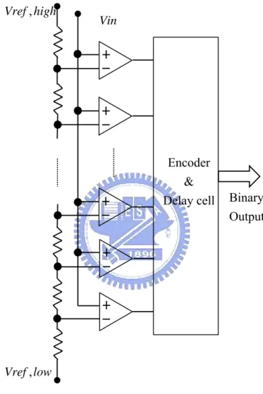
The conventional flash architecture is the simplest and fastest analog-to-digital converter. In a typical flash ADC, the analog input signal is simultaneously compared to reference voltages by a string of comparator circuits, as shown in Figure 2.1. As the input voltage increases, the comparators set their outputs to logic 1, starting with the lowest comparator. Think of the flash converters as being like a mercury thermometer.
As temperature increases, the mercury rises. Likewise, as the input voltage rises, comparators referenced to higher voltages set their outputs from 0 to 1. The thermometer code is encoded into binary code. The reference voltages are provided by connecting to a resistor string to generate the monotonic increase of reference voltages of full scale.
Vin high Vref , low Vref , Encoder &
Delay cell Binary Output
Figure 2.1 Conventional flash ADC architecture.
1 2N −
For an N-bit flash ADC, comparators and resistors are required. Flash ADCs are fast, but they have drawbacks. When resolution increases, the amounts of comparators and resistors grow exponentially, and they consume considerable power. As a result, most flash ADC studies have been focused on less than 8-bit resolution.
N
2
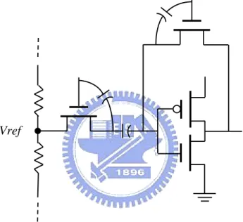
feed-through errors are the most popular. A primary factor determining the basic DC linearity of any flash ADC is the match that is obtained in the elements of the resistor divider. Matching of the resistor ladder elements is dependent on geometry in fabrication process. Analog MOS switches used for the reference and feedback switches, inevitably develop undesirable parasitic capacitances between the gate and source/drain terminals, as shown in Figure 2.2. When the MOS switches are turned off, transient currents flowing through the parasitic capacitances can alter the charge which is finally stored on the input coupling capacitor of the comparator. Charge feed-through may cause offset error and gain error in the conversion. [3]
Vref
Figure 2.2 Parasitic capacitors in CMOS switches.
2.2 Threshold Inverter Quantization
Flash ADC [4]-[8]
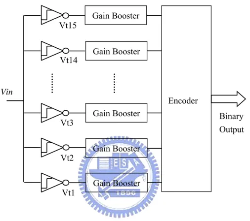
The conventional flash ADC is considered to realize the fastest conversion rate but it suffers from not only larger chip size and larger power dissipation, but also lower dynamic performance due to large input capacitance. Consequently, another simpler flash converter named TIQ flash ADC is proposed. Figure 2.3 shows the block diagram of 4-bit TIQ containing 15 comparators, gain boosters and an encoder.
The idea is to use the digital inverters with various threshold voltages as analog voltage comparators. The gain boosters make sharper transition of comparator output and provide full swing. The encoder converts the thermometer code to the binary code in two steps.
Figure 2.3 Block diagram of 4-bit TIQ.
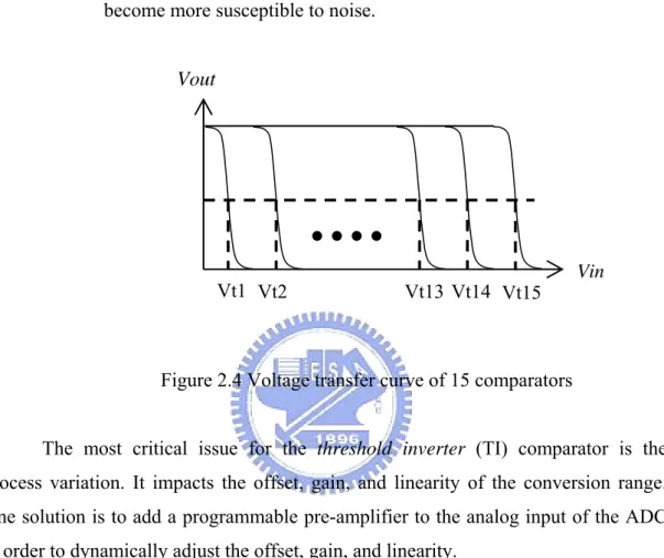
By adjusting the aspect ratio of inverters, we can get various threshold voltages. When we want a higher threshold voltage, we can enlarge the width PMOS or shrink the width of NMOS. We get lower threshold voltage in the opposite way. The various threshold comparators are arranged in parallel and monotonically, as shown in Figure 2.4. In conventional flash converters, the comparators are identical, while the comparators are different in the TIQ based flash ADC. The TIQ technique has many advantages:
(1) Simpler voltage comparator circuits. (2) Faster voltage comparison speed. (3) Elimination of resistor ladder circuits.
(4) Do not need switches, clock signal, and coupling capacitors. Gain Booster Gain Booster Gain Booster Gain Booster Gain Booster Vt1 Vt2 Vt3 Vt14 Vt15 Binary Output Encoder Vin
(5) Compatible with CMOS process, and ideal for SOC implementation. But it has two criteria to be carefully considered as following:
(1) ADC input range varies due to process parameter changing form one fabrication to another.
(2) An inverter is single ended, not differential, causing the ADC to become more susceptible to noise.
Vt1 Vt2 Vt13 Vt14 Vt15 Vout
Vin
Figure 2.4 Voltage transfer curve of 15 comparators
The most critical issue for the threshold inverter (TI) comparator is the process variation. It impacts the offset, gain, and linearity of the conversion range. One solution is to add a programmable pre-amplifier to the analog input of the ADC in order to dynamically adjust the offset, gain, and linearity.
Other issues for the TIQ flash ADCs are temperature variation, power supply variation, and single ended input noise. The former two problems can be solved by DSP solution; the later noise issue also can be solved by adding a single differential input amplifier to recondition the ADC input signal.
As compare to conventional flash converters, they have some characteristics in common, such as high-speed conversion and sensitive to process variation. But TIQ flash ADCs have advantages of lower power consumption and smaller chip penalty.
2.3 Modified TIQ Flash Converter
Architecture
As we mentioned in the previous section, the TIQ flash ADC has some merits in power consumption and small area. Further more, we want to enhance its high-speed characteristic and signal integrity. We replace the threshold inverters with tri-state inverters for power saving, and add inductive peaking circuits for high-speed performance. We take tri-state inverter based multiplexer (MUX) instead of cascading inverters for gain boosting. The modified TIQ flash ADC schematic is shown as Figure 2.5, and the design concepts is described as below.
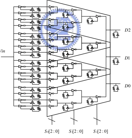
Vin 0 D 1 D 2 D ] 0 : 2 [ 0 S S1[2:0] S2[2:0] Figure 2.5 Schematic of the modified TIQ flash ADC.
2.3.1 Comparator Design
In 4-PAM transmission, we require three accurate comparators which equal to 2-bit ADC to convert 4-level signal. In order to achieve accurate performance for variable signals in 4-PAM transmission, we make sixteen floating comparators of monotonic threshold voltages in an ADC. We are going to select three accurate comparators among the floating comparators through calibration for the conversion. We replace inverters with tri-state inverters because they can be properly switched on or off. [9]
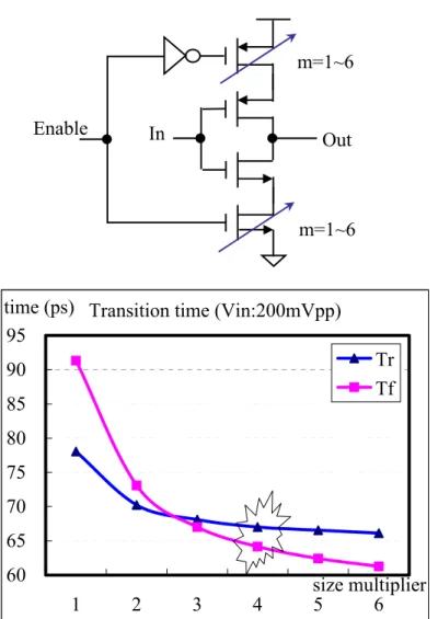
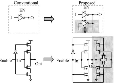
We take tri-state inverters as threshold comparators for the advantages of simple structure, high speed, low power, small area, and controllability. The unnecessary threshold comparators can be switched off to save power. We have a little overhead, but greatly improve power consumption. We put the enabling switches of tri-state inverters on the power side and ground side as shown in Figure 2.6. They can be pre-charged and perform better high frequency response. In this work, we set the conversion range from 600mV to 1200mV in the modified TIQ ADC. In addition, we attach the inductive peaking circuits at the output of comparators. It sacrifices gain but gets bandwidth to enhance high-speed performance. This will be discussed later.
Out Enable In M1 M2 M3 M4
2.3.2 Multiplexers [10]-[12]
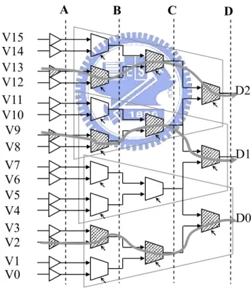
The comparator outputs connect the inputs of tri-state inverter based MUX and we have three multiplexers coinciding with the three selected comparators. Consider that 16 comparators corresponding to 24 inputs of multiplexers, there are partial overlaps for the sake of small signal coverage and accuracy. [13] The 8-to-1 MUX is composed of tri-state inverters, inductive peaking circuits, and control logics. The tri-state inverters work as gain booster, while inductive peaking components enhance high-speed characteristics. The MUX allows only one path which represents the matching comparator, and the control logics switch off the inactive tri-state inverters to save power as shown in Figure 2.7.
Figure 2.7 TIQ based ADC
Because tri-state inverter is the most used component in the circuits, needless to say, we must optimize it. We enlarge the width enabling MOS so that it drains larger current. Thus we get a multiplier of 4, and about 65ps transition time as shown in Figure 2.8. For signal balance consideration, we seek for the optimum of MOS sizing.
V0 V1 V2 V3 V4 V5 V6 V7 V8 V9 V10 V11 V12 V13 V14 V15 D2 D1 D0 A B C D
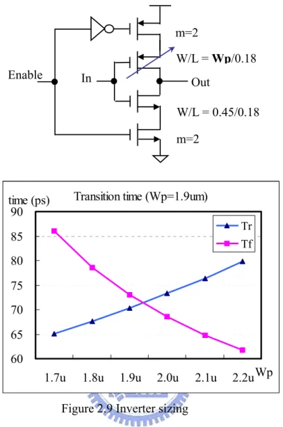
The crossing point in Figure 2.9 is the optimum for PMOS and NMOS. Only when pull-up current and pull-down current strike a balance, the tri-state inverter behaves well.
Figure 2.8 Enabling MOS sizing
Transition time (Vin:200mVpp)
60 65 70 75 80 85 90 95 1 2 3 4 5size multiplier6 time (ps) Tr Tf m=1~6 m=1~6 In Out Enable
m=2 m=2 In Out Enable W/L = Wp/0.18 W/L = 0.45/0.18
Transition time (Wp=1.9um)
60 65 70 75 80 85 90
1.7u 1.8u 1.9u 2.0u 2.1u 2.2uWp
time (ps)
Tr Tf
Figure 2.9 Inverter sizing
The MUX also has gain boosting effects due to cascading tri-state inverters shown in Figure2.10. Because of inductive peaking, we intentionally use a gain factor of 2. When receiving a decayed signal of 100mV swing, it is amplified stage by stage to 1600mV at the output of the MUX.
Figure 2.10 Gain boosting of TIQ based ADC
2.3.3 Inductive Peaking Circuits [14]-[15]
As we mentioned in the previous two sections, adding inductive peaking cells at the outputs of tri-state inverters can improve high-speed performance. The inductive peaking cells are identical in the MUX, while they are different in the threshold comparator bank accordingly. Each cell consists of a tri-state inverter and a resistor. The tri-state inverter is configured as diode connected by a resistor which is replaced with a transmission gate. In Figure 2.11, it shows the schematic of threshold comparator with and without inductive peaking component.
The short path between input and output of the tri-state inverter clamps at 0.9V of DC level. The connection of inductive peaking circuit lowers the output resistance of the tri-state inverter, and so does the gain. As a result, knee frequency increases as output resistance decreases. At low frequency, the output resistance is about
gm
1 ,
while it roughly equals to the resistance of transmission gate at high frequency. It is intended to design the resistance of transmission gate larger than
gm
1 , so it obtains
larger gain and extends bandwidth at high frequency. The broadband technique is inductive peaking. The Figure 2.12 is a “Gain-Bandwidth Plot” about inductive peaking. Because the circuits consume more power, we take tri-state inverters instead of inverters. Thus the inactive inductive cells can be properly turned off.
A B C D V0 V1 V2 V3 V4 V5 V6 V7 V8 V9 V10 V11 V12 V13 V14 V15 D2 D1 D0 A B C D
Figure 2.11 Schematic of inductive peaking circuits
Figure 2.12 Gain-Bandwidth plot of inductive peaking EN O I Out Enable In Out Enable In EN O Conventional Proposed I Conventional Proposed Ft1 Ft2 Frequency Gain
Chapter 3
Design of ADC Calibration
We realize calibration scheme by threshold voltage modulation. In other words, feeding a periodic signal to a comparator bank of various threshold voltages, it produces digital outputs of various duty cycles. The duty cycle is proportional to the portion of the threshold of input signal as shown in Figure 3.1. We randomly strobe the digital outputs to estimate the duty cycle of a channel by undersampling. After a great deal of counting, we can precisely obtain the duty cycle of the channel. Additionally, undersampling has a significant benefit: Power dissipation is proportional to clock rate, so we can save power by reducing the sampling frequency.
For a comparator array with the same input frequency, a larger swing has closer duty cycle outputs due to its sharper slope. The denser the duty cycles are, the more accuracy we will have in the calibration. So far as 4-PAM signal is concerned, the center between two levels is the best threshold voltage for conversion. In other words, the three ideal duty cycles of comparators should be 75%, 50%, and 25%.
Vth1 Vth2 Vth3 Vth4 Vth5 Vth6 Vth1 Vth2 Vth Vth Vth Vth Duty cycle = 0 % Duty cycle = 20 % Duty cycle = 40 % Duty cycle = 60 % Duty cycle = 80 % Duty cycle =100 % Periodic Input Signal Threshold Comparators Digital Outputs Duty Cycles
Figure 3.1 Threshold comparators and duty cycles
3.1 Schematics of Calibration
The calibration circuits consist of a duty cycle estimator, an absolute offset comparator, a minimum register, channel select registers, a channel select counter, a level select counter, and a controller. [16] The block diagram is shown in Figure 3.2.
Absolute Offset Comparator Duty Cycle Estimator Minimum Register Channel Select Register Level Select Counter Channel Select Counter Controller Mode State 9
ADC Channel Switches ADC Output
3.1.1 Duty Cycle Estimator
of a stimulus timer and a counter. The timer
3.1.2 Absolute Offset Comparator
nel is the closet to the target duty c
In Figure 3.3, this module is composed
is triggered by undersampling clock, and the counter is sampling data from MUX outputs synchronously. We can easily calculate the percentage of “one” which is so called “duty cycle” in the counting.
Figure 3.3 Schematic of duty cycle estimator
The absolute offset comparator judges which chan
ycle of a MUX. An easy way to find out the best channel is to compare their “distance” to the target. The “distance” here is the absolute difference between
CLK ... T_up SW Stimulus Timer Reset CLK ... SW One’s Counte Reset r T Q0 TFF > T Q1 TFF > T Q6 TFF > T Q0 TFF > T Q1 TFF > T Q7 TFF > D Q DFF >
sampled number and target number. So it is a digital comparator which compares the sampled value to the temporary minimum. When the absolute offset value is less than temporary minimum, the temporary minimum will be updated by the absolute offset value in the minimum register.
In Figure 3.4, “D” represents absolute offset value while “Q” stands for minimum value in the comparator cell. When counting number is less than the target, “INV” activates to make one’s complement for subtraction to get a positive value. The implementation of one’s complement is easier than that of two’s complement in digital system, but it has “one” error in one’s complement. When the sampling value is very large, this error can be ignored.
Figure 3.4 Schematic of absolute offset value D0 Compare D6 INV Absolute Offset Comparator Q D
3.1.3 Minimum Register
The minimum register is a “parallel in, parallel out” register as shown in Figure3.5. It reloads absolute offset value when “Less” signal triggers the data flip flops (DFF). To trigger it by “Less” signal can save more power than by clock signal, and avoid error of critical path delay from the comparator.
D0 DFF Less DFF DFF D1 Reset Minimum Register D6 Q0 Q1 Q6
Figure 3.5 Schematic of minimum register
3.1.4 Channel Select Counter / Registers
Duty cycle estimator evaluates the channels one by one through channel select counter. The channel select registers update the channel numbers when minimum register update occurs. Thus optimal channel numbers are stored in the registers after calibration. The schematics of channel select counter and register are configured as one’s counter and minimum register respectively in previous sections, but they have only 3 bits.
3.1.5 Level Select Counter
Level select counter is the same schematic as channel select counter. It makes an increment when the estimation of a MUX is finished. There are three threshold comparators to be determined through level select counter.
3.1.6 Controller
The calibration controller is built in combinational logics. It commands other function blocks to act and being triggered by them for state transition. The state machine tells the status of calibration and it is helpful to debug.
3.1.7 Self-calibrating PAM Receiver Architecture
The self-calibrating 4-PAM receiver includes two blocks: 2-bit ADC and calibration circuits. We build some control pins between the interfaces for testing considerations as shown in Figure 3.6. Such as manual switches for manually select channels, it helps us to test device characteristics and debug.
4PAM Data Comparator Array D0 D1 D2 S0 S1 S2 | + Manual switch Manual control Ref. Duty CSC LSC & Encoder CSR Clock Digital comparator Mode State Calibration Circuit 2-bit ADC Channel Selector Controller S2 register S1 register
S0 register Min- register .Duty Cycle Estimator
3.2 Flow Chart and State Diagram
The calibration flow as shown in Figure 3.7 can be viewed as three loops: small loop for stimulus timer, middle loop for channel select counter, and large loop for level select counter.
BEGIN
Y N
N
Calibration System reset
Y Channel END? N Y Channel increment N
Asynchronous duty cycle estimation begins
Y 1 0 Sampled value? K-Mode? Counting increment Time up? N Y Level END?
Update Min & CSR Minimum?
Level & Channel scan iteration begins
Optimum and target minimum comparison
Calibration END Level increment
3.2.1 Flow Chart
In Figure 3.7, calibration starts as long as it is switched to calibration mode, resetting counters and registers. Stimulus timer starts to count and one’s counter samples from ADC output during this period. When time is up, the sampled value is processed through absolute offset comparator and compared with minimum. The minimum register and channel select register are updated when new value is less than previous one. The single channel evaluation route is shown in Figure 3.8. After comparison, channel select counter makes an increment and goes on to next channel counting if it is not the last channel of the MUX. If it is, the first channel select register stores the optimal channel number of the MUX for 75% duty cycle, and the system loops back for the next threshold level. The channel route is shown in Figure 3.9. Repeat the same procedure till three threshold levels are done. The system will return to normal operation, if we switch to normal mode in any cases. And the default channel number of each MUX is configured as channel number 3, center of the channel number.
CLK Comparator Array S1 + Ref. Duty CS Counter Duty cycle estimation Digital Comparator Update Duty cycle evaluation END N Channel Duty Evaluation begins Y 1 0 Counting up Time is up? N Y Less? Stimulus timer Increment Sampled value? Update minimum register & channel register
Compare with previous minimum Estimated value subtracts
reference duty & make absolute value Channel Select MUX S1 register Minimum registe r |X|
Ch1 Ch2 Ch3 Ch4 Ch5 Ch6 Ch7 Ch8 CLK |X| + Ref. Duty CS Counter Duty cycle estimation Update Ch2 Ch8 Ch7 Ch1 ... Channel Select MUX Comparator Array N Y Overflow? Channel Select Counter resets Channel Select Counter Level calibration BEGIN Channel duty Evaluation start Channel Scan END S1 register Minimum register
3.2.2 Truth Table and State Diagram
The calibration flow is controlled by the controller. We fill out the transition table as shown in Table 3.1, and get excitation equations. By these equations, we complete the control logics.
PS S0 S0 S1 S2 S3 S3 S4 S5 S5 S6 S6 S7 S7 NS S0 S1 S2 S3 S3 S4 S5 S2 S6 S2 S7 S7 S0 PS 000 000 001 010 011 011 100 101 101 110 110 111 111 NS 000 001 010 011 011 100 101 010 110 010 111 111 000 Mode 0 1 1 1 1 1 1 1 1 1 1 1 0 T_up X X X X 0 1 1 X X X X X X CH_END X X X X X X X 0 1 X X X X Lev_END X X X X X X X X X 0 1 X X Reset 0 0 1 0 0 0 0 0 0 0 0 0 0 Reset_CH 0 0 1 0 0 0 0 0 0 1 1 0 0 Reset_T 0 0 0 1 0 0 0 0 0 0 0 0 0 CK_SW 0 0 0 1 1 1 0 0 0 0 0 0 0 CMPR 0 0 0 0 0 0 1 0 0 0 0 0 0 CH_in 0 0 0 0 0 0 0 1 1 0 0 0 0 Lev_in 0 0 0 0 0 0 0 0 0 1 1 0 0 Input Output State
Table 3.1 Truth table of the calibration
The state diagram is shown in Figure 3.10 and the notations represent controller inputs and outputs. There are total eight states in the calibration, and the state machine needs three DFFs to show up.
S2 Reset_T=1 CK_SW=1 S1 Reset_CH=1 Reset=1
Figure 3.10 State diagram of the calibration
S0 S3 CK_SW=1 S5 CH_in=1 S6 Reset_CH=1 Lev Mode=1 T_up=0 Mode=1 Mode=0 _in=1 S4 CMPR=1 Mode=1 CH_END=0 Mode=1 LS_END=0 S7 Mode=0 Mode=1 Mode=1 Mode=1 T_up=1 Mode=1 T_up=1 Mode=1 LS_END=1 Mode=1 CH_END=1 Mode=1
3.3 Statistical Analysis [17]-[19]
3.3.1 Random Variables
Bernoulli random variable can be modeled as a single coin toss. That is,
) (ξ A
I equals one if the event A occurs, and zero otherwise. is called the Bernoulli
random variable since it describes the outcome of a Bernoulli trial if we identify with a “success”, and
A
I
1 = A
I IA =0 with a “failure”. It is the value of the indicator
function for some event A; X=1 if A occurs, and X=0 otherwise. The Bernoulli random variable is shown in Equation 3.1.
A I ) 1 ( ] [ ] [ 1 0 1 } 1 , 0 { 1 0 p p X VAR p X E p p P p q P Sx − = = ≤ ≤ = − = = =
Equation3.1 Bernoulli random variable
Suppose that a random experiment is repeated n independent times. Let X be the number of times a certain event A occurs in these n trials. X is a random variable with range . For example, X could be the number of heads in n tosses of a coin and is called “binominal random variable”. It can be the number of success in n Bernoulli trials. The binominal random variable is shown in Equation 3.2. Discrete random sampling can be modeled as binominal random variable as well, thus we can apply to duty cycle estimation.
} , , 1 , 0 { n SX = K ) 1 ( ] [ ] [ ,.... 1 , 0 ) 1 ( } , , 1 , 0 { p np X VAR np X E n k p p P n S k n k n k k x − = = = − ⎟ ⎠ ⎞ ⎜ ⎝ ⎛ = = − K
3.3.2 Confidence Interval and Confidence Level
Based on central limit theorem, binominal distribution can be made for Gaussian approximation by normalizing with zero mean and unit variance. We estimate the required number of samples using the Gaussian approximation for the binominal distribution. Let be the relative frequency of A in n Bernoulli trials. The probability of interest is
) (n fA ⎟ ⎟ ⎠ ⎞ ⎜ ⎜ ⎝ ⎛ − − = ⎥ ⎥ ⎦ ⎤ ⎢ ⎢ ⎣ ⎡ − < ≅ < − ) 1 ( 2 1 ) 1 ( ] ) ( [ p p n Q p p n Z P p n f P A n ε ε ε
Equation 3.3 Confidence level of event A
The above probability cannot be calculated because p is unknown. However, it can be easily shown that p(1− p)≤14 for p in the unit interval. For such p, it follows that
2 1 ) 1 ( − p ≤
p , and since tail function Q(x) decreases with increasing argument.
(
)
⎥ ⎥ ⎥ ⎥ ⎥ ⎥ ⎥ ⎥ ⎦ ⎤ ⎢ ⎢ ⎢ ⎢ ⎢ ⎢ ⎢ ⎢ ⎣ ⎡ ⎟⎟ ⎠ ⎞ ⎜⎜ ⎝ ⎛ − + + − ≅ ∫∞ − = − ≥ < − π π π π π ε ε 2 2 1 1 1 2 2 2 2 2 2 1 ) ( 2 2 1 ] ) ( [ x x x e dt x t e x Q n Q p n A f P[ ]
( )
⎪ ⎩ ⎪ ⎨ ⎧ pdf the of tail the of y probabilit : interval accuracy desired : A event of y probabilit : x Q A P εEquation 3.4 Gaussian approximation for binominal probability and tail function Analyzing from Equation 3.4, we know that tail function Q(x) is a decreasing function containing two parameters. Definitely, either loose desired accuracy or more samples, we are more confident with the result due to higher probability. In other
words, we get more occurrences if we claim for loose boundaries or tolerances. Or we can make more experiments to concrete our conclusion for the accuracy. Figure3.11 shows the probability of event A with a confidence interval ε in a normal distribution.
ε
P[A]
x fA(x)
Figure 3.11 Confidence interval of probability
Instead of seeking a single value that we designate to be the “estimate” of the parameter of interest, we can attempt to specify an interval of values that is highly likely to contain the true value of the parameter. Find an interval [L(x), U(x)] such that
P [L (x) ≤ k ≤ U (x)] = 1 – α
This is, the interval contains the true value of the parameter with probability 1 – α. Such an interval is a (1 – α)×100% confidence interval, and (1 – α) is so called “confidence level” shown in Figure 3.11. The narrower confidence interval, the more accurately we can specify the estimation for parameter.
3.3.3 Samples and Accuracy
The number of samples and input signal amplitude are dependent with the accuracy of selecting comparators. For example, the larger the signal amplitude, the denser duty cycles at comparator outputs due to sharper waveform for a periodic frequency. As a consequence, we must have more samples to keep the same distinguishing ability. In accordance with statistics as we mentioned in previous sections, every sampling can be treated as Bernoulli trial, and successive Bernoulli trials are binominal random variables. Each comparator has its duty cycle as binominal variables in the estimation.
We are interested in how many samples and the confidence level we need for the conversion. More samples imply higher accuracy, but more hardware and
calibration time. Obviously they are trade-off. For a given signal, we evaluate the number of samples to maintain a certain confidence level so that we can select the optimal comparators. We configure the threshold gap of 40mV in the comparator array. It means that we have a resolution of 40mV. From table 3.2, for an input of 300mV swing, we can have over 99.35% confidence level in a 7-bit counter. Meanwhile, it equals that 95.45% confidence level for a 400mV swing. When the number of samples is larger, calibration time becomes longer and accuracy rises significantly.
Variance σ2= 1/4
accuracy ε x Q(x) N-bit timer # of samples confidence level
4.53 1.181E-05 5 32 100.00% 6.4 4.422E-10 6 64 100.00% 9.05 5.855E-19 7 128 100.00% 12.8 9.798E-37 8 256 100.00% 18.1 2.648E-72 9 512 100.00% 25.6 1.88E-143 10 1024 100.00% 36.2 9.33E-286 11 2048 100.00% 2.26 0.0227664 5 32 95.45% 3.2 0.0018694 6 64 99.63% 4.53 1.181E-05 7 128 100.00% 6.4 4.422E-10 8 256 100.00% 9.05 5.855E-19 9 512 100.00% 12.8 9.798E-37 10 1024 100.00% 18.1 2.648E-72 11 2048 100.00% 1.51 0.0881241 5 32 82.38% 2.13 0.0299467 6 64 94.01% 3.02 0.0032689 7 128 99.35% 4.27 3.652E-05 8 256 99.99% 6.03 4.273E-09 9 512 100.00% 8.53 5.515E-17 10 1024 100.00% 12.1 8.756E-33 11 2048 100.00% 1.13 0.1388265 5 32 72.23% 1.6 0.0771742 6 64 84.57% 2.26 0.0227664 7 128 95.45% 3.2 0.0018694 8 256 99.63% 4.53 1.181E-05 9 512 100.00% 6.4 4.422E-10 10 1024 100.00% 9.05 5.855E-19 11 2048 100.00% 0.75 0.1884185 5 32 62.32% 1.07 0.1478554 6 64 70.43% 1.51 0.0881241 7 128 82.38% 2.13 0.0299467 8 256 94.01% 3.02 0.0032689 9 512 99.35% 4.27 3.652E-05 10 1024 99.99% 6.03 4.273E-09 11 2048 100.00% 40/400 40/300 40/100 40/200 40/600
(Accuracy ε here is the ratio of threshold gap over input signal amplitude) Table 3.2 Estimation of samples and confidence level
Chapter 4
Simulation Results
We are going to discuss simulation results, specification comparison, and layout in this chapter. Simulation results include comparator corners, ADC output, and calibration results. We will check the ADC output before CDR processing and analyze the calibration result. Further more, we will make a specification comparison.
4.1 Threshold Comparator
4.1.1 Threshold Comparator Corners
Conversion range of comparator is set from 600mV to 1200mV. In Figure 4.1, FF case has the sharpest slope, and it means the dynamic range becomes wider for signal coverage. Because the number of comparators does not increase, obviously the threshold gap becomes wider and resolution deteriorates. In contrast, dynamic range of SS corner decreases, but resolution improves. That is to say, the accuracy is getting better in self-calibration. Another in SF case, the dynamic range shifts upward due to strong PMOS. FS case is on the opposite way, but both resolutions are the same as TT case. The calibration automatically selects the threshold comparators closet to center of the eye diagram, so we can avoid process variation impact to the accuracy through calibration.
Comparator threshold corner simulation 0.4 0.5 0.6 0.7 0.8 0.9 1 1.1 1.2 1.3 1.4 Wp/Wn Vth Vth_FF Vth_FS Vth_TT Vth_SF Vth_SS
4.1.2 Gain Boosting
We mentioned that the inverter based MUX has gain boosting effects in previous chapter. In Figure 4.2, an initial input is amplified stage by stage from 100mV to 1300mV, and biased at DC level of 0.9V. Besides, we can see a light transition overshoot due to inductive peaking in the eye diagram.
S 0[2:0] S 1[2:0] S 2[2:0] S 0[2:0] S 1[2:0] S 2[2:0]
A B C D
A B C D A B C
4.2 ADC Simulation
4.2.1 2.5Gsps 4-PAM Input
We input a 2.5Gsps 4-PAM signal of 600mV swing to TIQ ADC through a fading channel by RC model. The ADC input waveform is simulated as shown in Figure 4.3. We extract three best channels out of three threshold levels from the simulations. The best channels have at least 0.5 unit interval (UI) eye-opening of 400ps period at the ends of outputs as shown in Figure 4.4.
Figure 4.4 TIQ ADC output of 4-PAM input D2: Ch_11 Eye width: 225ps D1: Ch_8 Eye width: 215ps D0: Ch_3 Eye width: 260ps
4.2.2 2.5Gbps Pseudo Random Binary Sequence
(PRBS) Input
We input PRBS of different level to replace 4-PAM, and get the three best eye-diagrams of ADC output as shown in Figure 4.5. The eye-openings are more than 330ps in the post simulation.
D2: Ch_13 Eye width: 300ps D1: Ch_8 Eye width: 326ps D0: Ch_2 Eye width: 360ps
Figure 4.6 shows the FF case of PRBS input, and it has wider eyes than those of TT case. Threshold gap becomes wider in FF case, so the channels of best eyes are getting closer. D2: Ch_13 Eye width: 338ps D1: Ch_8 Eye width: 350ps D0: Ch_3 Eye width: 375ps
SS case as shown in Figure 4.7 stands opposite to FF case. The jitter grows due to slow transition, and outer channels for better eye-diagrams. Even though, the eye-opening is still enough for a CDR system.
D2: Ch_14 Eye width: 246ps D1: Ch_8 Eye width: 293ps D0: Ch_1 Eye width: 326ps
4.3 Calibration Simulation
For the sake of calibration verification, we simulate an 80MHz triangular input as fast as our available function generator. In Figure 4.8, we can see the calibrated channels of threshold levels and data outputs accordingly. With respect to Table 4.1, the selected threshold comparators are very close to ideal threshold voltages of eye center, and so do the duty cycles.
LS1 LS0 Lev 2 Lev 1 Lev 0 D2 D1 D0 CH 4 CH 7 CH 11
Level 0 Level 1 Level 2
Duty: 26%
Duty: 51%
Duty: 71%
345Msps 0.6~1.2V Ideal Vth Channel Vth duty% Level 2 1.05 11 1.04 26% Level 1 0.9 7 0.88 51% Level 0 0.75 4 0.76 71% 80MHz triangular
Table 4.1 Calibration summary
Corner Level 0 Level 1 Level 2
FF CH4 CH7 CH8
TT CH4 CH7 CH11
SS CH3 CH7 CH12
Table 4.2 Corner cases calibration result
Further more, we compare the calibration resulting different corners as shown in Table 4.2. As we expect, FF case has wider conversion range, so it selects the closer channels as compare with other corners. In contrast, SS case selects the outer comparators.
4.4 Layout
The PAM receiver was fabricated in a six-level metal single poly 0.18um CMOS process. The layout of this chip is shown in Figure 4.9. The core area is
( 2 111
0. mm 370um 300× um), while the total area is ( ).
The pads close to the circuit layout are configured for high-speed I/Os, however, the pads far away are designated for control pins. The rest area is filled up with decouple capacitance in order to bypass power noise.
2 25 . 1 mm 1120um 1120× um 1120 um 1120 um
4.5 Specification Comparison
As shown in Table 4.5, this specification falls into two categories: normal mode and calibration mode. In normal operation, we get eye-openings over 0.75UI for PRBS source and 0.5UI for 4-PAM source. The power dissipation is only 3.2mW and 4.2mW for 2.5Gbps PRBS and 2.5Gsps 4-PAM input respectively. While operating in calibration mode, it consumes 3.9mW at 345MHz sampling rate, and 5.16mW in the worst case. Notice that the power consumption of calibration can be reduced by decreasing sampling rate.
Item Spec (Normal) Spec (Calibration) Supply Voltage 1.8V
2.5Gbps PRBS
Input 80 MHz Triangular 2.5Gsps 4PAM
PRBS jitter 100ps@ 2.5Gbps N/A
4-PAM jitter 190ps@ 2.5Gsps N/A
Power consumption 3.2mW @ 2.5Gbps PRBS 4.2mW @ 2.5Gsps 4PAM 3.9mW @ 345MHz CLK 5.16mW @ FF Core area 0.111 2 mm Table 4.3 Performance summary
In Table 4.4, figure of merit (FOM) shows the comparison with the other high-speed ADCs. For the convenience of comparison at the same level, we scale up to 6bit and 8bit to obtain estimated 67mW and 268mW power respectively at 2.5Gsps. Obviously, this work has least power consumption based on the same resolution, and the second minimum area.
ADC Process Resolution Speed Power Area Year
TIQ [4] 0.25um 6bit 1Gsps 44mW 0.013mm2 2001
PRA-TIQ [20] 0.18um 6bit 2.66Gsps 97mW 0.218mm2 2004
Flash [21] 0.25um 6bit 1.3Gsps 600mW 0.12mm2 2003
Folding [22] 0.18um 8bit 1.6Gsps 774mW 3.6mm2 2004
Proposed 0.18um 2bit 2.5Gsps 4.2mW 0.11mm2 2006
Chapter 5
Measurement Considerations
In this chapter, we divide testing method into two parts: one is 4-PAM test, and the other is binary test. First, we introduce measurement considerations, inclusive of chip function implementation, and test configuration. Second, we illustrate how to generate signal sources in two ways: on-chip and off-chip test. Last, we describe both test flows.
5.1 Test Setup
5.1.1 Measurement Configurations
The test configuration is shown in Figure5.1 and we illustrate the purpose of each instrument. Power supply enables this chip, and pulse data generator provides stimulus input up to 5Gbps data rate. Dual-in-line (DIP) switches are used for channel selection, and switching mode. By a wide-band oscilloscope, we can observe the high-speed performance of ADC. Meanwhile, logic analyzer helps to check the calibrated channels and state. There is still an alternative way to measure channel characteristics by serial BERT. It stimulates the ADC and measures bit error rate (BER) with a feedback. [23]
Input Calibration Mode Clock Lev [2:0] State [2:0] Level Select [1:0] ADC Manual SW [8:0] D [2:0] 1 166770022BB L Looggiicc AAnnaallyyzzeerr A Aggiilleenntt NN44990011BB S Seerriiaall BBEERRTT A Aggiilleenntt 8866110000BB W Wiiddee--BBaanndd O Osscciilllloossccooppee A Aggiilleenntt 8811113300AA P Puullssee DDaattaa G Geenneerraattoorr Power Supply
5.1.2 Test Considerations
We illustrate the measure purpose of each pin, and explain what we want to observe as below:
1. MUX output: D [2:0]
These are the output signals of some channels of some channels after a series of gain boosting. We judge if it is clear enough to operate in 2.5GHz or even higher after clocked data recovery (CDR), and observe ISI jitter.
2. DFF output: Q [2:0]
These points are designated to observe the duty cycle after asynchronously random sampling. The sampled signal has only clock jitter, but no ISI jitter. 3. Level output: Lev [2:0]
These pins tell us which channel of each level we select by switching level select signal LS [1:0].
4. State machine: State [2:0]
By probing these pins, we realize current state of the system, and debug easier. 5. Manual channel select: MS [8:0]
In the system measurement, we can manually control the channel for calibration verification. We measure not only BER, but also eye-diagram.
6. Level select: LS [1:0]
To observe the selected channels, we switch it for three levels. 7. Auto:
It is a control pin for MUX switch interface. It enables for self-calibration, or disables for manual control otherwise.
5.2 Signal Sources
In this section, we introduce two methods to generate signal for test. One is a built-in circuit for both 4-PAM and binary signal sources, and the other is an off-chip solution.
5.2.1 On-chip Solution
This self-generating signal source consists of linear feedback shift registers (LFSR), multiplexers, logic gates, and a 2-bit current mode digital-to-analog converter (DAC) in the circuitry which is shown in Figure 5.2. It generates not only 4-PAM signal, but also PRBS signal. The PRBS generated by LFSR is fed into binary-to-thermometer decoder via MUX to control the gates of current mode DAC for 4-PAM signal. We insert control logics between LFSR and MUX for different level binary signals.
The current mode DAC can generate high-speed signal, but drain a great deal of current. By switching on the gates, it sinks more current and lowers the output voltage. For our specification, its output swing ranges from 600mV to 1200mV and speed is up to 2.5Gsps. To consider the termination, the pull-up load is 50 ohm. The schematic of 2-bit current mode DAC is shown in Figure 5.3.
Table 5.1 is the code table of switching patterns. As shown in Figure 5.4, the eye of 2.5Gsps 4-PAM signal is wide-open. Figure 5.5 shows self-generating 2.5Gbps PRBS of various levels.
16-bit LFSR Control Logic MUX 2:1 S0 S1 SW VOUT B [1:0] Binary 4-PAM 2 2 2 CLK CLK Binary-to-Thermometer Decoder
2-bit Current Mode DAC G [3:1] 3
Figure 5.2 Block diagram of signal generator
50 Ω M=32 M=21 M=19 M=54 G0 W=1u L=0.5u G1 G2 G3 500 Ω W=1u M=32 W=1u M=21 W=1u M=54 W=1u M=19 mA 24 . 0 IREF = ISINK IN V
Pattern 4-P M PRBS_0 PRBS_1 PRBS_2 PRBS_F A
SW 0 1 1 1 1
S1 X 0 0 1 1
S0 X 0 1 0 1
Table 5.1 Signal generator switching code table
PRBS_F
PRBS_2
PRBS_1
PRBS_0
Figure 5.5 Self-generating 2.5Gbps PRBS signal
5.2.2 Off-chip Solution
There still an alternative way to generate 4-PAM signal by analog MUX inputs attached to resistor ladder. We can apply high-speed analog MUX and make random switches for random 4-PAM signal as shown in Figure 5.6. The key spec summary of analog MUX is shown in Table 5.2.
LMH 6574
Pulse PRBS VIN
Parameter Description Condition Typ. value Unit
-3dB BW -3dB BW Vout =0.5Vpp 500 MHz 0.1dB BW 0.1 dB BW Vout = 0.25Vpp 150 MHz SR Slew Rate 4V step 2200 V/us T Channel switching time Logic transition to 90% output 8 ns RS OS Overshoot 2V step 5 %
5.3 Test Flow
5.3.1 Test Flow of 4-PAM Input
Test flow of 4-PAM input is shown in Figure 5.7. BEGIN Y N 4-PAM input Y Channel END? Y N Y Level END? Eye-diagram Measurement Calibration Verification Verification END Channel comparison Channel increment N N PRBS level increment Switch to Normal mode Calibration Mode Calibration END?
5.3.2 Test Flow of Binary Input
If we do not have 4-PAM source, there is an alternative way to replace 4-PAM with binary signal. First, it is fed with a PRBS which represents the lowest eye of 4-PAM signal while switching to calibration mode. After a period of calibration, we will get the selected channel number of the level. Record it and repeat the same procedure for the rest levels.
Second, we switch to normal mode when complete calibration is done, and feed the lowest binary sequence again and scan channels. It tells which channel is the best either by BER analysis or eye-diagram comparison. Last, we check the other two levels iteratively. The test flow is shown in Figure 5.8.
BEGIN Y N PRBS input Y Y N Y Calibration mode? Channel increment N Y Level END? BERT & Eye measurement Calibration Verification Verification END Channel comparison PRBS level increment & Record Channel increment N N PRBS level increment Level END? Switch to Normal mode Calibration END? Channel END?
Chapter 6
Conclusion
In this thesis, we have proposed an ADC with advantages of simple structure, high-speed, power-efficient, low hardware overhead, and immunity against process variation and temperature. We use tri-state inverters as comparator and building up multiplexers for the merit of power saving and gain and gain boosting. By proper overlap between comparators and multiplexers, we can enhance the accuracy of conversion. Because the threshold comparators are deeply impacted by process variation, we use an undersampling scheme for calibration. By means of duty cycle estimation, we can choose optimal comparators and channels for conversion. The numbers of sampling are evaluated by statistical analysis. For example, we can get 99.35% confidence level for a 300mV peak to peak input out of a 7-bit counter to acquire the best channels.
In verification, we propose PRBS and 4-PAM test. PRBS is a simpler way for data acquisition, but the test flow is more complicated for the three-eye iteration. As for 4-PAM source, we have on-chip and off-chip solutions. On-chip signal solution is a self-generating signal by LFSR and DAC. On the other hand, off-chip solution is configured as a resistor-ladder type DAC through a high slew rate analog MUX.
Bibliography
[1] R. Jacob Baker, "CMOS Mixed-signal Circuit Design", Wiley Interscience, 2003.
[2] Rudy van de Plassche, "CMOS Integrated Analog-to-Digital and Digital-to-Analog converters", 2nd, Kluwer Academic Publishers, 2003
[3] Michael J. Demler, "High-Speed Analog-to-Digital Conversion", Academic Press, 1991.
[4] Jincheol Yoo, Kyusun Choi, Ali Tangel, "A 1-Gsps CMOS Flash A/D Converter for System-on-Chip Application", IEEE Computer Society Workshop on VLSI, pages 135-139, April 2001.
[5] Jincheol Yoo, Daegyu Lee, Kyusun Choi, Ali Tangel, "Future-ready ultrafast 8bit CMOS ADC for System-on-Chip Applications", IEEE International ASIC/SOC Conference, pages 135-139, September 2001.
[6] Jincheol Yoo, Daegyu Lee, Kyusun Choi, Jongsoo Kim, "A Power and Resolution Adaptive Flash Analog-to-Digital Converter", ACM/IEEE International Symposium on Low Power Electronics and Design, pages 233-236, 2002.
[7] Daegyu Lee, Jincheol Yoo, Kyusun Choi, "Design Method and Automation of Comparator Generation for Flash A/D converters", IEEE International Symposium on Quality Electronic Design, pages 138-142, March 2002.
[8] Jincheol Yoo, Kyusun Choi, Jahan Ghaznavi, "Quantum Voltage Comparator for 0.07um CMOS Flash A/D Converters", IEEE Computer Society Annual Symposium on VLSI, 2003.
[9] R. Jacob Baker, "CMOS Circuit Design, Layout, and Simulation" , 2nd Edition, Wiley Interscience, 2005.
[10] Jan M. Rabaey, Anantha Chandrakasan, Borivoje Nikolic, "Digital Integrated Circuits, 3rd Edition", Prentice Hall, 1995.
[11] John P. Uyemura, "CMOS Logic Circuit Design", Kluwer Academic Publishers, 1999.
Interscience, 2002.
[13] Behzad Razavi, "Principles of Data Conversion System Design", Wiley Interscience, 1995
[14] Behzad Razavi, "Design of Analog CMOS Integrated Circuits", McGraw Hill International Edition, 2001.
[15] Behzad Razavi, "Design of Integrated Circuits for Optical Communications" , McGraw Hill International Edition, 2003.
[16] Neil H. E. Weste, Kamran Eshraghian, "Principles of CMOS VLSI Design ~A System Perspective", 2nd Edition”. Addison Wesley, 1993.
[17] Alberto Leon-Garcia, "Probability and Random Process for Electrical Engineering", 2nd Edition, Addison Wesley, 1994.
[18] Henry Stark, John W. Woods, "Probability and Random Process with application to Signal Process", 3rd Edition, Wiley Interscience, 2002.
[19] Roy D. Yates, David J. Goodman, "Probability and Stochastic Process" Wiley Interscience, 1999.
[20] Sunny Nahata, Kyusun Choi, Jincheol Yoo, "A High-Speed Power and Resolution Adaptive Flash Analog-to-Digital Converter ", IEEE International SOC Conference, pages 33-36, September 2004.
[21] Koen Uyttenhove, Michiel S.J. Steyart, Senior Member IEEE, "A 1.8-V 6-Bit 1.3-GHz Flash ADC in 0.25-um CMOS", IEEE Journal Solid-State Circuits, Vol 38, No 7, July 2003.
[22] Robert C. Taft, Senior Member IEEE, Chris A, Member IEEE, Maria Rosaria Tursi, Member IEEE, Ols Hidri, Member IEEE, Valerie Pons, "A 1.8-V 1.6-GSample/s Self-Calibrating Folding ADC With 7.26 ENOB at Nyquist Frequency", IEEE Journal Solid-State Circuits, Vol 39, No 12, December 2004.
[23] Mark Burns, Gordon W. Roberts, "An introduction to Mixed-signal IC test and Measurement", Oxford, New York, 2001.