國 立 交 通 大 學
電子工程學系 電子研究所碩士班
碩 士 論 文
具懸浮奈米線結構之新穎元件的
製作與特性分析
A Study on the Fabrication and
Characterization of Novel Devices with
Suspended Nanowire Structures
研 究 生:許家維
指導教授:林鴻志 博士
黃調元 博士
具懸浮奈米線結構之新穎元件的
製作與特性分析
A Study on the Fabrication and
Characterization of Novel Devices with
Suspended Nanowire Structures
研 究 生:許家維 Student:Chia-Wei Hsu
指導教授:林鴻志 博士 Advisors:Dr. Horng-Chih Lin
指導教授:
黃調元 博士
A
Dr. Tiao-Yuan Huang
國 立 交 通 大 學
電子工程學系 電子研究所碩士班
碩 士 論 文
A Thesis
Submitted to Department of Electronics Engineering & Institute of Electronics College of Electrical and Computer Engineering
National Chiao-Tung University in Partial Fulfillment of the Requirements
for the Degree of Master of Science
in
Electronics Engineering September 2010
Hsinchu, Taiwan, Republic of China
具懸浮奈米線結構之新穎元件的
製作與特性分析
研究生 : 許家維 指導教授 : 林鴻志 博士
研究生 : 許家維 指導教授 :
黃調元 博士
國立交通大學
電子工程學系 電子研究所碩士班
摘要
在本論文中,我們成功地製作兩種新穎的元件結構,分別為具懸浮奈米線通 道之薄 膜電 晶體 (suspended-NW-channel TFTs) 、 與垂直 式金 氧半 場效電 晶體 (VMOS)。其中,前者的懸浮奈米線通道、與後者的邊襯(sidewall spacer)閘極電極 皆利用一簡單、低成本的反應式離子蝕刻(RIE)技術製作完成。此外,在後者的製 作過程中,我們只使用兩個主要的微影光罩,以達到進一步降低成本的目的。 具懸浮奈米線通道之薄膜電晶體展現了極低的次臨界擺幅(subthreshold slope) (35 mV/dec.)、與相當大的遲滯窗口(hysteresis window) (3.7 V)。我們發現擺入 (pull-in)汲極電流限制效應、汲極電流的似暫態行為、非對稱低次臨界擺幅與遲滯 窗口打開的特性。除此之外,我們還發現,隨著幾何結構尺寸與閘極電壓掃描速 率的改變,遲滯窗口、擺入電壓(Vpi)、擺出電壓(Vpo)、擺入之低次臨界擺幅(S.S.F) 與擺出之次臨界擺幅(S.S.R)都有特定的變化趨勢。最後,依據以上所有的發現,我們提出一個觀念性的模型,用以描述元件操作時靜電力、彈性回復力與表面黏 滯力之間的交互作用。
另一方面,當操作在順向操作模式時,垂直式金氧半場效電晶體展現了良好
的開關電流比(106
)與可接受的抗貫穿能力(anti-punch through ability)。此外,我們 也發現一個有趣的兩段式開啟特性,並且解釋為凸邊角效應的結果。
A Study on the Fabrication and
Characterization of Novel Devices with
Suspended Nanowire Structures
Student : Chia-Wei Hsu Advisors : Dr. Horng-Chih Lin
Advisors :
Dr. Tiao-Yuan Huang
Department of Electronics Engineering and Institute of Electronics
National Chiao Tung University, Hsinchu, Taiwan
Abstract
In this thesis, we have successfully developed and fabricated two kinds of novel device structures, including suspended-nanowire (NW)-channel thin film transistors (TFTs) and vertical metal-oxide-semiconductor field-effect transistors (VMOS). The suspended NW channels in suspended-NW-channel TFTs and the sidewall spacer gate electrode in VMOS are formed by a simple and low-cost reactive ion etch (RIE) technique. Especially, in VMOS, further cost down could be achieved as only two main photolithographic reticles are needed through the process.
The suspended-NW-channel TFTs with ultra-low subthreshold swing (S.S.) (35 mV/dec.) and considerable hysteresis window (3.7 V) are demonstrated. The limited pull-in drain current (ID), the transient-like behavior in ID, the asymmetric S.S., and the
hysteresis window opening characteristics are also observed. Besides, the specific trends in hysteresis window, Vpi, Vpo, S.S.F and S.S.R with the change of geometric
structure dimensions and VG sweeping rate are found and analyzed. Finally, based on
all of the above observations, a conceptual model illustrating the interaction between the electrostatic force, the elastic recovery force and the surface adhesion forces during device operation is proposed.
On the other hand, the VMOS devices exhibit a good on-off ratio of 106 and acceptable anti-punch through ability. In addition, an interesting two-step turn-on characteristic is also observed and explained by the convex corner effect.
Acknowledgment
走到這裡,我在這個實驗室已經待了整整 26 個月了,出入 NDL 也早已屆滿一 週年,題目更是換了兩次。經歷了這麼多事情,一路上多虧許多貴人的相助,我才 能夠走完這顛頗的碩士生涯。 首先,特別感謝指導教授 林鴻志 教授、黃調元 教授。不管是在學術成就的 追求,或者實驗態度的分享,點點滴滴都帶給我許多的啟發。特別是在實驗不順利 時,林老師適時的提醒、指正,讓我少走了許多冤枉路,而妙語如珠的黃老師更是 讓壓力瞬間減少許多。謝謝你們。 當然 ADTL 的伙伴們,我是一定不會忘記你們的。感謝蔡子儀學長、蘇俊榮學 長、徐行徽學長、林哲民學長、陳威臣學長、林政頤學長以及李克慧學姐,在實驗 的設計、結果的分析都給我很大的幫助與指導。另外,在實驗進度捉襟見肘時、機 台狀況不穩時,及時的建議與安慰都讓我倍感溫馨。不能不提的是郭嘉豪學長。老 實說,我這一年多來的實驗並不怎麼順利,多虧你一路的幫忙才讓我能夠漸漸步上 軌道,但是也很抱歉這一年來我並沒有完成既定的目標,反而讓你白白承受了不少 壓力,雖然說什麼都沒辦法表達我的感謝,還是老話一句「謝謝」。631 的同伴們, 有你們的陪伴,我才能度過這跌跌撞撞的 14 個月。每次實驗遇到問題,多虧你們 的打氣讓我有繼續下去的動力;你們持續努力的精神更是我所仿效的楷模。感謝簡 敏峰、羅正瑋、劉禹伶、林庭輔、陳冠宇、陳冠智,你們讓枯燥的實驗有了火花; 你們讓無聊的量測變得有趣;你們讓沈寂的空氣多了生氣。謝謝你們。 另外,感謝 NDL 與 NFC 的一切。實驗機台讓論文終究可以完成,操作小姐與 工程師的配合,更讓進度得以前進。感謝 NDL 周家如小姐、范庭瑋小姐、魏耘婕 小姐、林婉貞小姐、陳琇芝小姐、徐台鳳小姐、趙子綾小姐、李春杏小姐、蕭明娟 小姐無數次的通融與協助,讓延宕的實驗進度得以加速。謝謝你們。 最後,感謝我的父母:許隆昌 先生、劉惠珍 女士,你們無私的付出讓我可以 無後顧之憂的向前邁進;感謝哥哥,讓我的求學路上感受到親情的溫暖;感謝室友 Jefferson、蠻頭、砲哥,無限的包容與體諒,以及毫無怨言的聽我吐苦水、講心事, 讓我有依靠的感覺;更要感謝小企鵝,妳的陪伴、分享與相互扶持是我最大的福份。 謝謝你們。 此論文,謹獻給所有曾經幫助我、鼓勵我,以及我所敬重、珍惜的師長、朋友 們。謝謝你們。 許家維 誌於 風城交大 2010 年 9 月Contents
Abstract (Chinese)……… i
Abstract (English)……… iii
Acknowledgment (Chinese)……… v
Contents……… vi
List of Figure Captions……… viii
List of Table Captions……… xiv
Chapter 1 Introduction………...
11-1 Overview of Vertical MOSFETs………. 1
1-2 Overview of Low Subthreshold-Swing Devices……… 3
1-2-1 Impact-ionization MOS (I-MOS)……….………... 4
1-2-2 Tunneling FET (T-FET)………...……….. 6
1-2-3 Suspended-gate MOSFET (SG-MOSFET)…...………. 7
1-2-4 Suspended-NW-channel Device...………... 9
1-3 Motivation………... 10
1-4 Organization of this Thesis………...……….. 11
Chapter 2 Device Fabrication………
122-1 Device Structure and Process Flow of Suspended-NW-Channel TFTs………….. 12
2-2 Device Structure and Process Flow of Vertical MOSFETs………. 13
2-3 Measurement Setup and Electrical Characterization……….. 16
Chapter 3 Electrical Characteristics of Suspended-NW-channel TFTs. 19
3-1 Basic Electrical Characteristics….……….. 19
3-2 Hysteresis Phenomenon……….. 20
3-2-1 Basic Hysteresis Characteristics……….. 21
3-2-2 Effects of Structure Dimension………... 24
3-2-3 Effects of VG Sweeping Rate……….. 27
3-2-4 Summary……….. 28
3-3 Operation Mechanism………. 28
Table Captions………... 31
Chapter 4 Electrical Characteristics of Vertical MOSFETs……… 32
4-1 Background….……… 4-2 Basic Electrical Characteristics………... 32 33 4-3 Discussion………... 35
Table Captions………... 37
Chapter 5 Conclusion and Future Work………... 38
5-1 Conclusion……….. 5-2 Future Work……… 38 40 References……… Figure Captions……… 42 46 Vita……… 87 Publication List………. 88
List of Figure Captions
Chapter 1
Fig. 1.1. The progressive growth of Intel’s CPU transistor counts per microprocessor [3]. ……….. 46 Fig. 1.2. The CPU transistor count and feature size trends [4]. ………. 47 Fig. 1.3. Evolution of device feature size and the resolution capability of exposure
tools with various exposure wavelength [6]. ………... 47 Fig. 1.4. Three major structures for the design of vertical MOSFETs, based on (a)
solid source diffusion, (b) epitaxial and (c) implantation, respectively. ….. 48 Fig. 1.5. The conduction mechanism of drain current at low drain bias [14]. ……... 49 Fig. 1.6. (a) Basic device structure and (b) band diagram in the ON/OFF state of
the n-channel I-MOS [16]. ………... 49 Fig. 1.7. Carrier distribution in space- and energy-scale in a device with 50
nm-long high-field region obtained from 1D Monte-Carlo simulation, superimposed on the energy band diagram of the simulated structure. (a) One electron with low energy is injected from the left end of the high-field region at random time τ1. (b) The first carrier then initiates the
impact ionization avalanche, and carrier number multiplies. However, with initially small number of carriers in the device, a strong random fluctuation is expected, until a reasonable number of carriers are present and overcome the randomness in carrier multiplication. (c) The carrier multiplication continues at an average rate [23]. ………. 50 Fig. 1.8. Simulated and experimental source-drain breakdown voltage, VBr, versus
gated channel length, LG, curves for both n-type and p-type I-MOS [24].
The difference between n-type and p-type I-MOS is originated from dopant diffusion. The p-type dopant usually diffuses more extensively than the n-type one. ……….. 50 Fig. 1.9. Schematic view of T-FFT device structure. ………. 51 Fig. 1.10. Energy band diagram for gate-controlled BTBT in T-FET with 100 nm
Fig. 1.11. (a) Typical 3D structure of SG-MOSFET with anchors at both ends of SG suspended over the gate oxide layer [29]. (b) An equivalent electrical circuit of SG-MOSFET, i.e., a combination of electrostatically actuated NEMS switch and inversion-mode MOSFET [30]. ………. 52 Fig. 1.12. The 2D cross-section of SG-MOSFET. The SG-MOSFET is controlled by
two competing forces, electrostatic force and elastic force [29]. ………… 53 Fig. 1.13. The operation principle of SG-MOSFET. (a) As VG<Vpi, the electrostatic
force is balanced by elastic force only. (b) As VG>Vpi, the electrostatic
force overcomes the elastic force and the SG will be connected with gate oxide layer. There is no air gap anymore. [29]……… 53 Fig. 1.14. Typical ID-VG characteristics of SG-MOSFET for VD = 50 mV. Region 1
represents the weak inversion regime and Region 2 represents the electromechanical pull -in of mobile gate after reaching the non-equilibrium point. (Symbols: measurement results; Solid Line: analytical simulation). [30] ……….. 54 Fig. 1.15. The mechanical hysteresis cycle of an SG-MOSFET [30]. ………. 54 Fig. 1.16. The major fabrication steps of the suspended poly-Si NW channel device
with side-gated configuration [20]. (a) Gate definition. (b) Gate dielectric deposition, poly-Si channel deposition and S/D implantation. (c) S/D definition. (d) Air gap formation. ………. 55 Fig. 1.17. The basic electrical characteristics of suspended NW channel device [20]. 55
Chapter 2
Fig. 2.1. Key fabrication steps of suspended NW channel TFTs. (a) The top view of the suspended NW channel TFTs. (b) Formation of in-situ doped poly gate. (c) Deposition of silicon nitride, TEOS and α-Si channel with SPC. (d) Formation of S/D regions and sidewall spacer NW channels by RIE. (e) Channel region definition and S/D implantation. (f) Air gap formation. Note that, figures in (b) to (f) are cross-sectional view from the cutline
AB in (a). ………... 56
Fig. 2.2. The cross-sectional TEM images of suspended NW channel from the cutline AB indicated in Fig. 2.1 (a) with different over-etch time. (a) 28
sec. (b) 22 sec. ……….. 57 Fig. 2.3. The top view of suspended-NW-channel TFT taken by SEM. ……… 58 Fig. 2.4. Key fabrication steps of SG-VMOS devices. (a) The top view of
SG-VMOS device. (b) Vertical channel patterning by anisotropic plasma etching. (c) Re-oxidation and tilt sidewall channel implantation. (d) Formation of dry oxide, silicon nitride and TEOS gate dielectric stack and
in-situ doped poly gate. (e) Sidewall spacer gate electrode formation by
RIE. (f) Removal of exposed TEOS layer by DHF wet etching and S/D implantation. (g) Air gap formation. Note that, figures in (b) to (g) are cross-sectional view from the cutline AB in (a). ………. 59 Fig. 2.5. The top view of patterns in SEM bar region (a) and device region (b) after
vertical channel definition taken by in-line SEM. The physical channel length is 0.5 μm. ……….. 60 Fig. 2.6. The simulated total doping concentration profile in our SG-VMOS with
50 nm sacrificial TEOS layer. The device channel length is 0.5 μm. (a) Along cutline AB shown in Fig. 2.1. (b) Along y direction with x = -0.24 μm. (c) Along x direction with y = 0.57μm. ………... 61 Fig. 2.7. The ion implantation projection range (a) and standard deviation of
projection range (b) of various common dopants in crystalline silicon tilted and rotated to simulate a random direction [39]. ……… 62 Fig. 2.8. The in-line SEM images of the device patterns after sidewall spacer gate
definition and DHF wet etching. (a) and (b) show the right-hand side and left-hand side images of the device structure, respectively. The device channel length is 0.5 μm. ………. 63 Fig. 2.9. The in-line SEM images of the patterns in the device region after sidewall
spacer gate definition and DHF wet etching. (a) and (b) show the right-hand side and left-hand side images of the device structure, respectively. The device channel length is 1 μm. ……… 63
Chapter 3
Fig. 3.1. Figure 3.1. ID-VG curves of (a) conventional TFT and (b)
suspended-NW-channel TFT. ……….. 64 Fig. 3.2. The plot of S.S. versus ID for the devices with three different structures,
i.e., without sacrificial TEOS layer, before stripping the TEOS layer and
after stripping the TEOS layer. ……… 65 Fig. 3.3. The electrical parameters of a suspended-NW-channel TFT including the
pull-in voltage (Vpi), the pull-out voltage (Vpo) and the S.S. under the
forward and reverse sweeping measurements. ……… 65 Fig. 3.4. Schematic showing the definition of structural parameters of the
suspended-NW-channel TFTs including the channel length and the S/D extension length. ……….. 66 Fig. 3.5. The hysteresis characteristics of a suspended-NW-channel TFT under
consecutive forward and reverse sweeping measurements. ………. 66 Fig. 3.6. The plot of S.S. versus ID for a suspended-NW-channel TFT under
consecutive forward and reverse sweeping measurements. ………. 67 Fig. 3.7. The endurance characteristics for a suspended-NW-channel TFT under
consecutive cycling measurements. ………. 67 Fig. 3.8. The hysteresis curves of a suspended-NW-channel TFT measured before
(i.e., as fresh) and after 120 times cyclings. ……… 68 Fig. 3.9. The hysteresis curves of the suspended-NW-channel TFTs with channel
length of 0.4 μm, 1 μm and 5 μm, respectively. ……….. 68 Fig. 3.10. The hysteresis curves of the suspended-NW-channel TFTs with S/D
extension length of 0.25 μm and 0.5 μm, respectively. ………... 69 Fig. 3.11. The plot of hysteresis window versus channel length for the
suspended-NW-channel TFTs with S/D extension length of 0.25 μm and 0.5 μm, respectively. ……… 69 Fig. 3.12. T h e p l o t o f Vp i a n d Vp o v e r s u s c h a n n e l l e n g t h f o r t h e
suspended-NW-channel TFTs with S/D extension length of 0.25 μm and 0.5 μm, respectively. ……… 70 Fig. 3.13. Th e pl ot of S .S.F and S.S .R versus channel l ength for the
suspended-NW-channel TFTs with S/D extension length of 0.25 μm and 0.5 μm, respectively. ……… 70 Fig. 3.14. The hysteresis curves of the suspended-NW-channel TFTs with two
different NW thicknesses. ……… 71 Fig. 3.15. The plot of hysteresis window versus channel length for the
Fig. 3.16. T h e p l o t o f Vp i a n d Vp o v e r s u s c h a n n e l l e n g t h f o r t h e
suspended-NW-channel TFTs with two different NW thicknesses. ……… 72 Fig. 3.17. Th e pl ot of S .S.F and S.S .R versus channel l ength for the
suspended-NW-channel TFTs with two different NW thicknesses. ……… 72 Fig. 3.18. The hysteresis curves of the suspended-NW-channel TFTs with air gap
thickness of 100 nm, 80 nm, 30 nm and 10 nm, respectively. ………. 73 Fig. 3.19. The plot of hysteresis window versus air gap thickness for the
suspended-NW-channel TFTs. ………. 73 Fig. 3.20. Th e pl ot of Vp i an d Vp o v ers u s ai r ga p t hi ckn es s for t he
suspended-NW-channel TFTs. ………. 74 Fig. 3.21. The plot of S.S.F and S.S.R versus air gap thickness for the
suspended-NW-channel TFTs. ………. 74 Fig. 3.22. The hysteresis curves of the suspended-NW-channel TFTs operated at
different sweeping speed by modulating the increment of VG per step. ….. 75
Fig. 3.23. The plot of hysteresis window versus the increment of VG per step during
measurements for the suspended-NW-channel TFTs. ………. 75 Fig. 3.24. The plot of Vpi and Vpo versus the increment of VG per step during
measurements for the suspended-NW-channel TFTs. ………. 76 Fig. 3.25. The plot of S.S.F and S.S.R versus the increment of VG per step during
measurements for the suspended-NW-channel TFTs. ………. 76 Fig. 3.26. Various operation states of the suspended NW channels for the
suspended-NW-channel TFTs. (a) The NW channels are suspended and separated from the gate with the air gap. (b) As VG = Vpi, the central
region of the NW channels begins to contact with the gate stack. (c) As VG is further increased to turn the device into the ON state, most of the
NW channels are in contact with the gate stack. ………. 77 Fig. 3.27. Various operation states of the suspended-NW-channel TFTs. A: The NW
channels are suspended. B: The central region of NW channels begins to contact with the gate stack. C: Portion of the NW channels in contact with the gate stack gradually increases. D: ON state. E: The surface adhesion forces maintain the contact of NW channels with the gate stack, and the drain currents remains relatively high. F: The NW channels gradually detach from the gate stack. ……….. 78
Chapter 4
Fig. 4.1. The bias configurations of our VMOS devices with no TEOS layer under the forward and reverse operation modes, respectively. ……….. 79 Fig. 4.2. ID-VG curves of VMOS devices under forward operation mode with
nominal channel length of (a) 0.5 μm and (b) 1 μm. ………... 80 Fig. 4.3. The top-view of the VMOS with convex corner regions circled. ………… 81 Fig. 4.4. (a) The equivalent circuit of VMOS with two different MOSFETs in
shunt. The device 1 is with a lower Vth and better S.S. than device 2. (b)
The corresponding ID-VG curves of these two shunted MOSFETs. (c)
ID-VG curves of the equivalent shunt circuit. ………... 82
Fig. 4.5. Output characteristics of the VMOS operated under forward mode with nominal channel length of (a) 0.5 μm and (b) 1 μm. ………... 73 Fig. 4.6. ID-VG curves of VMOS devices under forward and reverse operation
modes with nominal channel length of (a) 0.5 μm and (b) 1 μm. ………… 84 Fig. 4.7. Output characteristics of the VMOS operated under the forward and
reverse modes with nominal channel length of (a) 0.5 μm and (b) 1 μm. ... 85
Chapter 5
Fig. 5.1. The top-view of modified SG-VMOS device layout. ……….. 86 Fig. 5.2. Schematic view of modified SG-VMOS device structure with epitaxial
List of Table Captions
Chapter 2
Table 2.1. Split table for suspended-NW-channel TFTs. ……….. 18 Table 2.2. Split table for SG-VMOS. ………... 18
Chapter 3
Table 3.1. Comparisons of electrical parameters between the conventional NW TFTs and suspended-NW-channel TFTs. ……….. 31 Table 3.2. Variance trend of electrical parameters with an change in structural
parameters and VG sweeping rate. (Symbols: ↑: increasing, ↓: decreasing,
−: no obvious variance). ……….. 31
Chapter 4
Table 4.1. The average value of various electrical parameters extracted from 32 nominally identical VMOS devices. ……… 37
Chapter 1
Introduction
1-1 Overview of Vertical MOSFETs
For decades, very-large-scale-integration (VLSI) metal-oxide-semiconductor field effect transistors (MOSFETs) are being continuously scaled down in critical dimensions (CDs) due to the needs of higher package density, higher device operation speed, better integrated circuit (IC) functionality and lower fabrication cost per unit. In 1965, the Intel’s co-founder Gordon E. Moore observed and predicted, which later became the famous Moore’s Law, “The complexity for minimum component costs has increased at a rate of roughly a factor of two per year [1].” The combination of Moore’s Law and Dennard’s scaling methodology [2] has provided industry with many generations of smaller, faster and higher performance microprocessors. According to the announcements from Intel Corporation, the number of transistors on microprocessor chips has grown explosively fast and is rising above the billion transistor level in recent years, as shown in Fig. 1.1 [3]. Figure 1.2 shows the central processing unit (CPU) transistor count and feature size trends [4].
In order to keep pace with the Moore’s Law, conventional planar MOSFETs inevitably faces a lot of challenges, such as high leakage current, severe short channel effects (SCEs), threshold voltage adjustment and other parasitic issues. In addition to all the issues stated above, there is one intrinsic problem people have to overcome first,
that is the limitation of photolithography. According to the Rayleigh’s theory, the resolution of a lithography system is proportional to the wavelength of light [5]. In other words, the shorter the light wavelength is, the higher resolution of lithography system is. Figure 1.3 shows device trends and resolution performance of exposure tools from 1970 to 2005 and beyond [6]. Starting with g-line of wavelength 436 nm, exposure tools have been shifting to shorter exposure wavelengths which agree with Rayleigh’s theory. In past decades, many researchers have dedicated themselves to developing new lithographic techniques in order to succeed the old one for continuous scaling. Nonetheless, to this date, advanced or next generation photolithography, namely, the extreme UV (EUV) system, is too expensive and not mature yet [7]. Hence, some of the research activities have been shifted to finding alternative routes for maintaining the scaling trend. One of such brilliant ideas is the transformation of device structures, such as vertical channel MOSFETs, i.e., vertical MOS (VMOS), to avoid the limitation of photolithography technology [8-11].
The major advantage of VMOS is that short channel length or small memory cell area could be achieved and well defined sub-lithographically by the film thickness. The reduction in reliance on advanced lithographic tools makes VMOS a promising candidate for future device structure constructed on a chip, whether in memory or logic application. Some research also had pointed out that the VMOS had an area advantage of 2.4 fold over equivalent planar MOS device [9]. In addition, VMOS combined with double gate or gate-all-around (GAA) structure could lead to a better gate control ability over the planar counterparts [12].
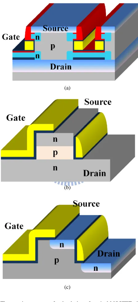
Figure 1.4 shows three main concepts for the design of vertical MOSFETs. In Figs. 1.4 (a) and (b), VMOS based on outdiffusion of dopants from deposited layers and on epitaxial layers are shown. However, in these approaches the fabrication
processes become much more complex due to the needs of complicated layer sequences. Another shortcoming for the structure shown in Fig. 1.4 (b) is the lack of substrate body contact to avoid kink effects. In contrast, different from the former two approaches, the one shown in Fig. 1.4 (c) based on implantation has some unique advantages. First, it has a simpler process comparable to planar device. Besides, substrate body contact is available to avoid floating body effect.
1-2 Overview of Low Subthreshold-Swing Devices
As mentioned above, the IC development trend follows the Moore’s Law. Hence, the power supply voltage should go down with the scaling of CDs due to the reliability and power consumption issues. Under this situation, a device with a low subthreshold swing (S.S.) is imperative to sustain a high on-state current (Ion) with an acceptable low
off-state current (Ioff). Furthermore, from the point of view of power consumption, it is
also very important to improve S.S. In modern IC chips, there are millions of devices in a single circuit. Such a huge IC chip implies an extremely large off-sate current may exist, resulting in serious concern with power wasting [13].
However, for conventional planar MOS transistors, the S.S. encounters some physical limitation. The following equation describes the mathematical definition and analytical form of S.S. based on well-established MOS theory,
1 . . 2.3 2.3 log d G G ox D s C V kT V kT S S C I q q , (Eq. 1-1)
where
V
G is the gate voltage,I
D is the drain current, k is the Boltzmann factor, T is the temperature, q is the quantity of electric charge,
s is the surface potential ofcapacitance [14].
It is well known that there are two main drain current (ID) conduction mechanisms
in MOSFETs, namely, diffusion and drift [15]. As we can see from Fig. 1.5 [14], in the subthreshold regime, the diffusion one dominates. In this regime, inversion carriers at the source side may overcome the potential barrier between source and channel region and then diffuse to the drain side. Moreover, the number of inversion carriers that could overcome the barrier and involve in the following process are limited by a thermodynamic factor “kT
q ” originated from Fermi-Dirac distribution [15]. Based on
this conduction mechanism, the subthreshold current is exponentially proportional to the gate voltage (VG) which is certainly consistent with the above equation. In ideal
case, at room temperature, the S.S. of conventional planar MOSFETs cannot be lower than 60 mV/decade.
In recent studies, some novel devices structure have been proposed to achieve a sub-60 mV/decade S.S., such as impact-ionization MOS (I-MOS) devices [16-17], tunneling FET (T-FET) [18], suspended-gate MOSFET (SG-MOSFET) [19] and suspended-nanowire (NW)-channel devices [20-22]. In the following part of this section, these devices are briefly reviewed.
1-2-1 Impact-ionization MOS (I-MOS)
One of the interesting ultra-low S.S. device structures is impact-ionization MOS, denoted as I-MOS, and its corresponding band diagrams in ON/OFF operation states are shown in Fig. 1.6 [16]. As we could observe from Fig. 1.6, there are three major differences between I-MOS and conventional MOSFETs. First, the doping types in source and drain region are opposite for I-MOS. Second, the conduction channel is essentially intrinsic. Third, for the channel in I-MOS, there are two electrically
different regions, gated and non-gated region.
The operation principle of I-MOS is based on the impact ionization mechanism. At the OFF state, the gate bias is lower than threshold voltage and the leakage current is dominated by the reverse current of the P-I-N diode. As the gate bias is higher than threshold voltage, I-MOS is operated at ON state. The gate bias lowers the potential level in the gated region of channel and develops a high-field junction near the source side, as shown in Fig. 1.6 (b). At this moment, the electrons injecting from source side would obtain enough energy to trigger the impact ionization process and lead to avalanche breakdown. Since the switch mechanism of I-MOS is not dominated by p-n junction barrier lowering, the S.S. could theoretically be reduced to below 60 mV/decade.
However, there exist some intrinsic issues for I-MOS. One is about time delay. Figure 1.7 shows the whole process for carrier multiplication in I-MOS from OFF state to ON state [23]. From this figure, we could comprehend that it indeed requires certain amount of time for device to fully turn on. And this time delay is related to the number of initial carriers at OFF state which is proportional to OFF state current level. The lower OFF state current level implies less initial carriers and results in longer time delay for carrier multiplication and turning on of the device. Therefore, the time delay for an I-MOS would become an obstacle for high speed dynamic switch application.
The other critical issue for I-MOS is non-scalable operation voltage. Figure 1.8 shows the source-drain breakdown voltage, VBr, versus gated channel length, LG, for
both n-type and p-type I-MOS [24]. For long-channel devices, the VBr decreases
linearly with LG. But as LG shrinks to 50 nm or shorter, VBr becomes a constant and do
not vary with LG. In order to explain this phenomenon, we need to know the key
ionization boundary and ionization coefficients. For long-channel devices, as LG
shrinks, the exponentially increase in ionization coefficients due to the rising of field strength is predominant over the linearly decreased boundary and causes VBr to fall
with reducing LG. In the case of short-channel devices, however, free carriers do not
have enough space to generate a sufficient number of impact ionization events to trigger breakdown. Hence, the only way for effectively increasing the average carrier energy is to increase the bias. Some simulation results have declared that VBr may
bounce back as LG is shorter than 20 nm [24]. The concern is that I-MOS probably
loses its transistor function as the channel length is scaled to such ultra-short dimension.
1-2-2 Tunneling FET (T-FET)
The device structures for I-MOS and T-FET are similar, both with a reverse biased P-I-N diode structure. For T-FET, the intrinsic channel is completely overlapped by the gate, however, so there is no non-gated channel region. Figure 1.9 shows a schematic view of T-FET.
Contrary to the I-MOS which uses the impact ionization as the current control mechanism, the major conduction process for on-state operation of T-FET is gate-controlled band-to-band-tunneling (BTBT) at the source side. The surface tunnel junction is at or near the cross-point of gate oxide/channel/source region. Figure 1.10 shows the energy band diagram of T-FET operated at ON (dashed line) and OFF (solid line) states [18]. With sufficiently high positive gate bias, so called n-type T-FET operation, the potential in the channel region will be pulled downward, electrons will tunnel from the valence band of p+ source region to the conduction band in the channel and flow to the n+ drain region. Similarly, as gate bias is sufficiently negative, the
T-FET will operate at p-type mode and the surface tunnel junction is shifted from p+ side to n+ side. At this time, the potential in the channel region will be pulled upward, electrons will tunnel from the valence band in the channel to the conduction band of n+ doped region (drain) and the generated holes will flow to the p+ doped region (source). This is for p-type T-FET operation, and highlights the ambipolar operation capability of the T-FET device. For the OFF state when the gate voltage is in the intermediate value between the p- and n-type operations so the surface band bending of the channel is not significant, due to the nature of intrinsic substrate, the field strength in the channel region is weak and thus a wide tunneling barrier is formed for both holes and electrons, as shown in Fig.1.10. The wide tunneling barrier limits not only direct tunneling but also thermal emission, making it difficult for electrons to move from the p+ region to the n+ region and therefore a low leakage current than conventional MOSFETs.
Simulation results show that T-FET can be scaled to at least 20 nm channel length with a slightly increased leakage current [25]. Moreover, the tunneling effect and the velocity overshoot may enhance the operation speed. However, the limited drive current density of T-FET becomes the biggest problem for its future application, owing to the fact that the depth of the surface tunneling junction is in the range of 10 nm or below [25]. There are some possible methods that could relieve this drawback, such as using higher source doping concentration, thinner gate oxide, more abrupt doping profile, and SiGe/Ge material [26-28].
1-2-3 Suspended-gate MOSFET (SG-MOSFET)
Another kind of low-subthershold swing device is the SG-MOSFET. A typical 3D structure of SG-MOSFET is shown in Fig. 1.11(a), with anchors on both ends of the
gate which is suspended over the gate oxide layer [29]. The major difference between regular MOSFET and SG-MOSFET is that the latter has an air gap between the suspended gate (SG) and real gate oxide layer. Equivalently, it could be viewed as a combination of an electrostatically actuated nanoelectromechanical system (NEMS) switch and an inversion-mode MOSFET [29]. An equivalent electrical circuit is shown in Fig. 1.11(b).
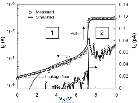
Next, we use Fig. 1.12 and Fig. 1.13 to illustrate the operation principle of SG-MOSFET. Because of the low dielectric constant of air gap and thus large effective oxide thickness (EOT), the SG-MOSFET has an extremely low gate leakage current as the transistor is operated at OFF state. When we apply a positive gate bias (for n-type SG-MOSFET) and increase it gradually, a positive charge will gradually build up in the gate electrode, and, for charge neutrality, there are also some negative charges induced on the substrate surface. Such a charge distribution forms an attractive electrostatic force between them which tends to pull the gate toward the gate oxide layer, as shown in Fig. 1.13(a), resulting in a narrowing of air gap thickness. One particular feature of the SG-MOSFET is that air-gap reduction provides a non-constant increment of gate capacitance with VG, so that ID increases super-exponentially in
weak inversion regime [30]. A typical ID-VG characteristic of n-type SG-MOSFET for
VD = 50 mV is shown in Fig. 1.14. Note that there is an intrinsic elastic force for each
material that may balance such an electrostatic force. Owing to this elastic force, SG will not connect with the channel until the electrostatic force becomes larger than some critical value. This critical value in gate voltage bias is called pull-in voltage (Vpi). As
the gate bias is larger than Vpi, the electrostatic force overcomes the elastic one, and the
SG will collapse onto the gate oxide layer, and an abrupt increase of drain current happens due to the increase of gate capacitance and the lowering of threshold voltage
[31], as shown in Fig. 1.13(b). Another outstanding feature of SG-MOSFET is its mechanical dynamic threshold voltage: high in the pull-in state and low in the pull-out state leading to a mechanical hysteresis phenomenon as shown in Fig. 1.15 [30].
These interesting behaviors of SG-MOSFET make it attractive for future device structure. Many researchers have worked on it and tried to apply it to many different areas, such as MEMS [19], memories [19, 30] and sensors [32-34].
1-2-4 Suspended-NW-channel Device
In the last part of this section, we introduce the suspended-NW-channel devices which were originally proposed by our group, Advanced Device Technology Laboratory (ADTL), at National Chiao-Tung University (NCTU). As shown in Fig. 1.16 [20], the fabrication process is simple, low-cost and compatible with nowadays CMOS technologies, compared with the three previously mentioned low-subthreshold swing devices because no advanced lithography tools or processes are involved.
The basic device structure of suspended-NW-channel devices, shown in Fig. 1.16 (d) [20], and the operation principle are similar to the SG-MOSFETs [22]. Both of them are with a suspended object over the air gap and operated mainly by the competition of electrostatic force and elastic force which are modulated by the gate bias exerted on the suspended object. However, the electrical characteristics are slightly different from the SG-MOSFETs [20-22], shown in Fig. 1.17 [20]. For example, the abrupt transition between ON and OFF states is not so straightforward in the suspended NW channel devices [20]. The structural differences in terms of the composition and dimensions of the suspended object are postulated to be the causes for the above disparity. Nevertheless, the suspended-NW-channel devices appear to be a promising idea. The major advantage includes its simple, self-aligned and gate-first
process. Besides, the suspended-NW-channel devices can be formed with sub-100 nm air gap simply by a buffered oxide etchant (BOE) wet etching step. Such a thin air gap is conducive to further scaling of the operation voltage.
1-3 Motivation
As we have learned from previous sections, issues in both the CD scaling and the non-scalability of S.S. have become major challenges for nowadays CMOS technology. To deal with the above issues, in this thesis, we divide our study into two main parts,
i.e., the investigation of the suspended-NW-channel thin film transistors (TFTs) and the
development of a novel SG-type device.
First, we focus on examining and clarifying the unique electrical characteristics of the suspended-NW-channel TFTs. In our previous works, devices with ultra-low S.S. were fabricated successfully [20-22]. However, many interesting characteristics the devices exhibit, such as the gradual turn-on behavior, oscillation of S.S., effects of NW channel dimensions, the asymmetric S.S. in hysteresis measurements and so on, are not clear and worth exploring [20-22]. Hence, in this thesis, we try to make some inductive inference from our data. In addition, the air gap thickness effect and some other interesting characteristics which are similar to the behaviors displayed by the SG-MOSFETs are also investigated.
Second, we also take advantage of the ultra-low S.S. in SG-MOSFETs and the exemption from advance lithography systems in VMOS to develop a new device structure. Here, we call it suspended-gate vertical channel MOSFET (SG-VMOS), a device structure combining the features of VMOS and SG-MOSFET. In addition to the intrinsic advantage of SG-VMOS, in our work, further cost down could be achieved thanks to the proper design of process flow which uses only two main
photolithographic reticles. Note that, compared with the suspended NW channel devices, we have changed the suspending material from undoped poly-Si to the conductive heavily doped one in the SG-VMOS. In this thesis, we will examine the basic electrical characteristics of VMOS and propose process adjustment suggestions to improving the basic characteristics of VMOS and SG-VMOS.
1-4 Organization of This Thesis
In this thesis, a general background of VMOS and low S.S. devices are introduced in Chapter 1. In Chapter 2, complete device fabrication process flows of suspended NW channel TFTs and SG-VMOS, and relevant measurement setup are described. In Chapter 3, some interesting characteristics of the suspended NW channel TFTs are examined and clarified. In Chapter 4, basic electrical characteristics of the fabricated VMOS are presented and discussed. Furthermore, in Chapter 5, we summarize the major observations in this study and make brief conclusions. Finally, some suggestions are given for future work.
Chapter 2
Device Fabrication
2-1 Device Structure and Process Flow of
Suspended-NW-channel TFTs
Figure 2.1 (a) shows the top view of the device. The cross-sectional views of the device along the cutline AB indicated in Fig. 2.1(a) in key fabrication steps of the fabrication are shown in Figs. 2.1 (b) to (f). All the devices in this section are fabricated on 6-inch bare silicon substrates capped with a 250 nm wet oxide.
First, a 150 nm in-situ n+ doped polycrystalline silicon layer was deposited by low pressure chemical vapor deposition (LPCVD) at 550 ℃ and defined as the gate electrode [Fig. 2.1 (b)]. After a standard clean process, a 20 nm silicon nitride layer and a 10 nm, 30 nm, 80 nm or 100 nm sacrificial TEOS oxide layer were deposited at 780 ℃ and 700 ℃, respectively. Next, a 100 nm amorphous silicon layer (α-Si) was deposited at 550 ℃ successively. All these films were deposited with LPCVD. Afterwards, a solid phase crystallization (SPC) treatment was performed at 600 ℃in N2 ambient for 24 hours to transform the silicon film from amorphous phase into
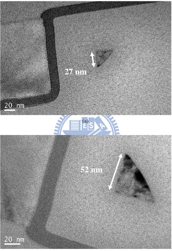
polycrystalline phase [Fig. 2.1 (c)]. With a photolithography step and the over-etching-time-controlled reactive ion etching (RIE) technique, the source/drain (S/D) regions and sidewall NWs were defined simultaneously [Fig. 2.1 (d)]. Here, the
over etching time is the major parameter for determining the dimensions of NW channels. Figures 2.2 (a) and (b) show the cross-sectional transmission electron microscopy (TEM) images of suspended NW channel from the cutline AB indicated in Fig. 2.1 (a) with over-etch time of 28 sec (thin NW) and 22 sec (thick NW), respectively. Thereafter, an additional photoresist (PR) layer was covered on the suspended-channel region followed by the phosphorous S/D ion implantation at 15 keV with a dose of 5×1015 cm-2 [Fig. 2.1 (e)]. Note that, the PR-covered channel region became the effective NW channels in our devices. For the dopant activation and the device passivation, a 400 nm TEOS layer was deposited on the entire wafer by LPCVD at 700 ℃. After a contact hole opening step with the aid of 160 ℃ hot H3PO4 and BOE
wet etching processes to remove the surface capping nitride and oxide, respectively, typical device fabrication was accomplished.
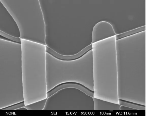
To further suspend the NW channels, a BOE wet etching process was performed to remove the sacrificial TEOS layer between the NW channels and the silicon nitride gate dielectric layer. Here, the high BOE etching selectivity between LPCVD TEOS and LPCVD silicon nitride could avoid the direct contact of NW channels and the gate electrode after the wet etching step. As a result, an air gap was formed and the suspended-NW-channel TFTs were accomplished [Fig. 2.1 (f)]. Table 2.1 summarizes the split conditions of our suspended-NW-channel TFTs. Figure 2.3 shows the top view of suspended-NW-channel TFT taken by scanning electron microscope (SEM).
2-2 Device Structure and Process Flow of Vertical
MOSFETs
As a quick start, Fig. 2.4 (a) shows the top view of VMOS layout and the remaining figures shown in Fig. 2.4 are the cross-sectional views along the cutline
AB indicated in Fig. 2.4(a).
First, we used 6-inch n-type (100) bare silicon as starting wafers. The resistivity of substrates was in the range of 2 to 7 Ω‧cm. After a conventional photolithography process, we applied a Cl2/HBr/O2-based anisotropic plasma etching step [35-38] to
define the vertical channel [Fig. 2.4 (b)]. The etched depth would roughly determine the dimension of the channel length. But the real electrical channel length would depend on the S/D junction depth and sidewall spacer gate width, as we would mention later. Certain amount of polymer would be formed on the sidewalls of patterns during the dry etching process, so a post-SC-1 clean was used to clean the sidewalls. Figure 2.5 shows the in-line SEM images of our patterns in the SEM bar region and device region just after the vertical channel definition. Because any surface roughness and etch-induced damage left on the sidewalls may cause severe mobility degradation and lead to a reduction in on-current, a 30 nm sacrificial thermal oxide was grown on the surface to smooth the channel surface and remove the damage sites.
Before removing the sacrificial oxide layer, we performed a phosphorous ion implantation at 170 keV with a dose of 4×1012 cm-2 to dope the channel [Fig. 2.4 (c)]. In this step, the sacrificial oxide layer mentioned above served as a screen oxide to prevent channeling effect in single-crystalline substrates. Note that, the above ion implantation step was carried out at a tilt angle of 45°, a twist angle of 72°, and the wafer was rotated 4 times to realize sidewall implantation. Afterwards, the sacrificial (screen) oxide was removed.
Thereafter, we performed the RCA clean and formed the gate stack on the surface. First, a 4 nm dry oxide was grown at 800 ℃ on the channel surface as a buffer layer. Next, a 9 nm silicon nitride layer was deposited by LPCVD at 780 ℃. And then a sacrificial TEOS oxide layer with thickness of 50 nm or 80 nm was deposited at 700 ℃
by LPCVD successively. Finally, a 150 nm in-situ n+ doped polycrystalline silicon layer was deposited at 550 ℃ as the gate material [Fig. 2.4 (d)]. Note that, all the high temperature and long thermal processes above may enhance the diffusion of channel dopants. Figure 2.6 shows the simulation results of total doping concentration profile in our devices with 50 nm TEOS sacrificial layer. In this simulation, we took into account all thermal budgets including subsequent S/D annealing.
Afterwards, the second mask of our process was applied to define gate electrode [Fig. 2.4 (e)]. By using the Cl2/HBr-based RIE technique combined with an etching
endpoint detector, we could form the sidewall spacer gate electrode which would serve as the suspended gate later in our SG-VMOS. Before S/D ion implantation, a diluted hydrofluoric acid (DHF) wet etching was performed to etch the exposed TEOS oxide layer. Note that it was a delicate step for lowering the S/D implantation energy and acquiring much abrupt S/D junctions. As shown in Fig. 2.7, too high an implantation energy would result in a broader doping profile and deeper S/D junction depth [39]. Figures 2.8 and 2.9 show the in-line SEM images of our patterns in the device region after sidewall spacer gate definition and DHF wet etching. Subsequently, a self-aligned S/D ion implantation was carried out by implanting BF249+ ions vertically with energy
of 25 keV and dose of 5×1015 cm-2, and activated by a spike rapid thermal annealing (RTA) at 1000 ℃ [Fig. 2.4 (f)]. Next, for device passivation, a 400 nm TEOS layer was covered on the entire wafer by plasma enhanced chemical vapor deposition (PECVD). Finally, contact hole opening was accomplished by a series of wet etching steps. The top passivation layer, silicon nitride gate dielectric and thermal oxide buffer layer were removed by immersing wafers in BOE, 160 ℃ hot H3PO4 and BOE solutions in
sequence, and a typical VMOS was thus accomplished. Table 2.2 summarizes the split conditions of our VMOS devices.
Note that to form our SG devices, an additional step was necessary. Specifically, a BOE wet etching process was performed to remove the TEOS layer between the sidewall spacer gate and gate dielectric layer. As mentioned previously in Section 2-1, the silicon nitride layer between the thermal buffer oxide and the TEOS oxide layer served as an etching stop layer by taking advantage of the high BOE etching selectivity between LPCVD TEOS and LPCVD silicon nitride. After that, an air gap was formed and the gate was suspended over the vertical channel [Fig. 2.4 (g)]. Note, in this step, the TEOS overlapped by the gate pad region was also etched simultaneously. However, the area overlapped by the gate pad was much larger than that covered by the sidewall spacer gate, so that a well-controlled etching time would remove the TEOS area covered by the sidewall gate completely, while leaving most of the TEOS under the gate pad region untouched. Thus a SG-VMOS was finally realized.
2-3 Measurement Setup and Electrical Characterization
The current-voltage (I-V) characteristics were evaluated by an automated measurement setup constructed by an HP 4156A precision semiconductor parameter analyzer, an Aglient TM 5250A switch, and the Interactive Characterization Software (ICS). During all measurements, the temperature was controlled at a stable value by temperature-regulated chuck.
For the electrical characterization, some important electrical parameters could be extracted from the ID-VG curves according to their definitions [15]. Here, we will
illustrate the definitions of the subthreshold slope (S.S.), transconductance (gm) and
threshold voltage (Vth).
First, the S.S. can be calculated from the subthreshold currents in the weak inversion region by
. . log G D V S S I . (Eq. 2-1)
Second, the gm is extracted by the differentiation of drain currents over gate
voltages, i.e., D m G D V const I g V . (Eq. 2-2)
Third, the Vth is calculated by the gm maximum method with drain bias of -50 mV
to ensure device operating in the linear region. As we know, the ID-VG curves deviate
from a straight line at gate voltages below Vth due to subthershold currents and above
Vth due to series resistance and mobility degradation effects. So, it is common practice
to find the point of maximum slope on the ID-VG curves by the maximum in the
transconductance. In practice, we fit a straight line to the ID-VG curve at that point and
extrapolate to ID = 0. The intersect point is defined as
V
Gi. Next we apply the followingequation to calculate Vth [40].
/ 2
th Gi D
Table Captions
Table 2.1. Split table for suspended-NW-channel TFTs.
Wafer Number 01 02 03 04 05 06 07 08 Over Etching Time
(sec)
22 ☆ ☆ ☆ ☆ ☆
28 ☆ ☆ ☆
Air Gap (TEOS) Thickness (nm) N/A ☆ ☆ 10 ☆ 30 ☆ ☆ 80 ☆ 100 ☆ ☆
Table 2.2. Split table for SG-VMOS.
Wafer Number 01 02 03 04 05 06 Nominal Channel Length
(μm)
0.5 ☆ ☆ ☆
1 ☆ ☆ ☆
Air Gap (TEOS) Thickness
(nm)
N/A ☆ ☆
50 ☆ ☆
Chapter 3
Electrical Characteristics of
Suspended-NW-channel TFTs
3-1 Basic Electrical Characteristics
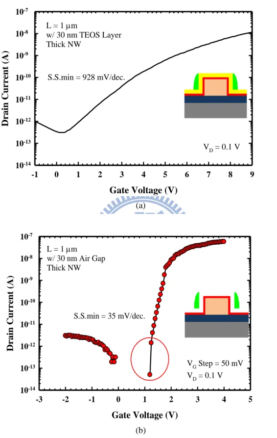
Figures 3.1 (a) and (b) show the ID-VG curves of a conventional NW TFT and
suspended-NW-channel TFT. As indicated in Figs. 3.1 (a) and (b), the conventional TFT and the suspended-NW-channel TFT refer to the one without and with the air gap structures, respectively. It can be seen that the suspended-NW-channel TFT depict a surprisingly low minimum S.S. of 35 mV/dec. compared with a mediocre 928 mV/dec. for the conventional counterpart. Apparently, the minimum S.S. is significantly improved for devices with suspended structure, despite their larger nominal EOT due to the lower dielectric constant of air over the TEOS oxide. Specifically, the suspended-NW-channel TFTs are having a gate dielectric stack of 30 nm air/ 20 nm silicon nitride and the nominal EOT of 128.14 nm. In contrast, for the conventional TFTs, the gate dielectric stack consists of 30 nm TEOS/ 20 nm silicon nitride with a nominal EOT of 41.14 nm. Figure 3.2 shows the plot of S.S. versus subthreshold ID for
a device without sacrificial TEOS layer (i.e., with 20 nm silicon nitride only), and devices before and after stripping the TEOS layer (i.e., the conventional TFT and
suspended-NW-channel TFT, respectively). Among these three device structures, the suspended-type one shows the best minimum S.S. throughout the subthreshold regime which further implies that the operation mechanism is not that straightforward. According to our previous results [20-22], such unusually small S.S. is referred to the electro-mechanical action of the suspended NW channels. The operation principle of NW channels in the suspended-NW-channel TFTs are mentioned in Subsection 1-2-4 and our previous work [20-22]. A detailed discussion will be presented later in Sections 3-2 and 3-3. In addition, such an unusually small S.S. also results in the lowering of Vth,
extracted by the constant current method [40], between the conventional devices and the suspended-NW-channel ones shown in Figs. 3.1 (a) and (b). Furthermore, the suspended-type devices exhibit a lower OFF state current, defined as the corresponding ID at VG = 0 V, which is advantageous in terms of reliability and power consumptions.
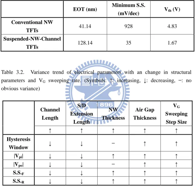
Table 3-1 shows the comparisons of electrical parameters between the conventional TFTs and suspended-NW-channel TFTs including nominal EOT, Vth and minimum
S.S.
3-2 Hysteresis Phenomenon
In order to investigate the operation principle of the devices, in this section, detailed discussion on the hysteresis phenomenon in the suspended-NW-channel TFTs under consecutive forward and reverse sweeping measurements is presented including the examination of the effects of the structure dimensions, gate voltage sweeping rate, and other factors that may affect the hysteresis characteristics. Before starting our discussions, some electrical and structural parameters are defined in Fig. 3.3 in which typical hysteresis curves of the suspended-NW-channel TFTs are shown. These electrical parameters include the pull-in voltage (Vpi), pull-out voltage (Vpo), forward
sweep S.S. (S.S.F), reverse sweep S.S. (S.S.R) and the hysteresis window. Among them,
the hysteresis window is defined as the Vth difference between the forward and reverse
sweeping measurements extracted by constant current method [40] at a constant drain current of 5×10⁻¹⁰ A, and Vpi and Vpo are defined as the VG corresponding to the
occurrence of pull-in and pull-out, respectively, of the suspended NW channels. Finally, S.S.F and S.S.R are extracted from the forward and reverse subthreshold regions,
respectively, with a roughly stable value, different from the minimum S.S. mentioned previously. For the structural parameters, the definitions of the S/D extension length and channel length are shown in Fig. 3.4. With the aids of the following observations, the operation mechanism of the suspended-NW-channel TFTs is illustrated in Section 3-3. Note that, all the electrical characteristics presented in this section are for the suspended-NW-channel TFTs under consecutive forward and reverse sweeping measurements.
3-2-1 Basic Hysteresis Characteristics
Figure 3.5 shows typical hysteresis curves for the suspended-NW-channel TFT with channel length of 0.4 μm and air gap thickness of 80 nm under specified operation conditions. An ultra-low minimum S.S. of 58 mV/dec. and a hysteresis window of 3.7 V are recorded. In the forward sweeping measurement, as VG increases and reaches Vpi,
a jump in ID is observed. This is an indication of pull-in action that the suspended NW
channels begin to contact the gate nitride due to the attractive electrical force exerted by the gate voltage. This leads to a dramatic decrease in EOT and thus a large increase in ID. However, dissimilar to most previous works in the SG-MOSFETs [19] that the
S.S. can be smaller than 10 mV/dec., in the present case, the S.S. is only slightly smaller than the ideal 60 mV/dec. due to the fact that the increase in ID is limited, so
the transition between the ON state and the OFF state is not abrupt. In other words, the turn-on behavior in our devices is gradual, in contrast to the sudden switching phenomenon presented in previous studies [19]. Based on such observation, it is postulated that, in the beginning of the contacting action, only the central region of the NW channels are in contacted with the gate stack, so the potential barrier away from the central region of the NW channels are still high resulting in a limited ID and a
non-abrupt transition behavior.
When ID reaches a level between 1×10⁻⁷ A and 1×10⁻⁹ A, the variances of ID with
the VG modulation become non-smooth in both the forward and reverse sweeping
directions, as shown in Fig. 3.5. This feature is in strong contrast to the characteristics of the conventional device shown in Fig. 3.1(a). As we will illustrate and explain later, in the suspended-NW-channel TFTs, the variances of ID with the VG modulation are
dependent on two completing mechanisms, i.e., the mechanical action of the suspended NW channels and the field-effect action of the conventional TFTs. In this case, for the devices operated at the current level below 1×10⁻⁹ A, the former one is dominating. For the devices operated at the current level higher than 1×10⁻⁷ A, the later one becomes the dominant mechanism. However, in the inter-level, both mechanisms are comparable in strength leading to a transient-like behavior in ID-VG curves. This
phenomenon was also referred to as the S.S. oscillation phenomenon in our previous work [22]. An example is given in Fig. 3.6 which shows the plot of S.S. versus ID for
devices under the forward and reverse sweeping measurements, respectively.
Another interesting phenomenon in the suspended-NW-channel TFTs is the asymmetric S.S. between the forward and the reverse sweeping measurements. As we can see from Fig. 3.6, the S.S.F (~230 mV/dec.) extracted in the ID range from 10-11 A
of the static force balance, for the pull-in action of the suspended NW channels, only the elastic recovery force and the electrostatic force are involved. However, as we sweep the VG in reverse, the pull-out action of the NW channels is impeded further by
the additional adhesion forces [29, 41], resulting in the worse S.S. in the reverse sweeping measurement.
Figure 3.7 shows the endurance characteristics for the suspended-NW-channel TFTs under cycling measurements. Apparently, after 120 times of operation cycles, the hysteresis window is enlarged. Besides, the hysteresis window opening is observed in our measurements from 1.82 V to 2.7 V. Figure 3.8 shows the ID-VG curves of the fresh
device and the device after 120 times of operation cycles. There is no obvious S.S. degradation in both forward and reverse sweep measurements, so the Vth shift is not
originating from the variances of the S.S. As reported by various groups [42-44], the shift of Vth is a signature of the charge trapping in the dielectric layer. As VG reaches
Vpi, the suspended NW channels are pulled in and make contact with the gate stack, a
sudden increase in ID occurs. After cycles of operation electrons are trapped in the
nitride layer. This would result in an increase in Vpi. This means it needs a larger gate
voltage to induce electrons in the channel for pull-in action. Such a result is reasonable since the nitride is a well-known electron trapping layer for SONOS flash devices. However, the above inference seems not reasonable in explaining the decreasing Vpo
after cycles of operation. That is, the electrically attractive force between the channel and the gate is weakened with the aforementioned electron trapping phenomenon and thus Vpo should increase as Vpi does, rather than decrease. The exact reason for the Vpo
is still under investigation. One possible explanation is the decline in force constant of the suspended channel with increasing operation cycles. Fatigue of the movable object’s elasticity will reduce the restore force and therefore, a delay in pull-out action
is resulted.
3-2-2 Effects of Structure Dimensions
In this subsection, we will present a detailed discussion about the influences of device dimensions on the hysteresis characteristics in the suspended-NW-channel TFTs. The device dimensions with which we are dealing include the channel length, the S/D extension length, the NW thickness and the air gap thickness.
Figures 3.9 and 3.10 show the hysteresis curves of the suspended-NW-channel TFTs with different channel length and S/D extension length, respectively. For the devices with a given 0.5 μm S/D extension length and 100 nm air gap, as the channel length increases from 0.4 μm to 5 μm, the Vpi, hysteresis window and the ON current
decrease accordingly, as shown in Fig. 3.9. The elastic constant of the NW channels in the devices with shorter channel length is larger, leading to a larger Vpi and the earlier
detachment of the NW channels from the gate stack. However, it is difficult to find out the specific VG corresponding to the starting moment of the NW channel’s pull-out
action, i.e., the pull-out point, simply from the electrical characteristics. Note that, the Vpo is treated as the corresponding VG at the moment of fully detachment of NW
channels from the gate stack. In Fig. 3.9, Vpo is defined as the VG when the ID drops to
the level dominated by the off-state leakage. It is found that the Vpo is smaller as the
channel becomes shorter. In addition, the smaller contact area between the NW channels and the gate stack during operation in the devices with shorter channel length also results in the worse S.S.F and S.S.R. Figures 3.11, 3.12 and 3.13 show the plots of
hysteresis window, Vpi, Vpo, S.S.F and S.S.R, respectively, versus channel length for
devices with two different S/D extension lengths (see Fig. 3.4). Apparently, as the S/D extension length shrinks to 0.25 μm, the variance in the hysteresis window, Vpi, Vpo,
S.S.F and S.S.R with channel length become unobvious. Despite these facts, there are
significant differences in various electrical parameters between devices with the S/D extension length of 0.5 μm and 0.25 μm, as shown in Fig. 3.10. The device with S/D extension length of 0.25 μm is with a higher Vpi and worse S.S. in both sweep
directions than its counterpart with 0.5 μm S/D extension length. Note that the total length of the suspended object is roughly the sum of the length of the suspended channel and the S/D extension. The difference between the two devices shown in Fig. 3.10 is postulated to be originated from the larger elastic constant and the smaller contact area in the device with shorter (0.25 μm) S/D extension, therefore it needs a larger electrically attractive force to overcome the elastic force. Furthermore, the 0.25 μm one is also with a lower ON current. This implies that the portion of the 2-m-long undoped suspended channels in contact with the gate nitride in the ON state is smaller for the device with shorter (0.25 μm) S/D extension.
Figure 3.14 shows the hysteresis curves of devices with different NW dimensions which are controlled by the over-etching time. The longer over-etching time will form NWs with smaller dimension (denoted as “thin” in the figure). Figures 3.15, 3.16 and 3.17 show the plots of hysteresis window, Vpi, Vpo, S.S.F and S.S.R, respectively, versus
channel length for devices with two different NW dimensions. Apparently, the devices with thinner NW channels are with better S.S. in both the forward and reverse sweeping measurements due to the larger contacted area compared with the ones with thicker NW channels, as shown in Fig. 3.17. In addition, Vpi in the devices with thinner
NW channels is also slightly lower, as shown in Fig. 3.16. These two observations imply that the thinner NW channels are with smaller elastic constant and thus smaller elastic forces as compared with the thicker counterparts. The higher flexibility of the thinner NW channels also result in a slightly higher ON current despite the larger
![Figure 1.2. The CPU transistor count and feature size trends [4].](https://thumb-ap.123doks.com/thumbv2/9libinfo/8224823.170692/63.892.133.748.165.1035/figure-cpu-transistor-count-feature-size-trends.webp)
![Figure 1.5. The conduction mechanism of drain current at low drain bias [14].](https://thumb-ap.123doks.com/thumbv2/9libinfo/8224823.170692/65.892.238.646.188.476/figure-conduction-mechanism-drain-current-low-drain-bias.webp)
![Figure 1.8. Simulated and experimental source-drain breakdown voltage, V Br , versus gated channel length, L G , curves for both n-type and p-type I-MOS [24]](https://thumb-ap.123doks.com/thumbv2/9libinfo/8224823.170692/66.892.147.736.378.1040/figure-simulated-experimental-source-breakdown-voltage-versus-channel.webp)
![Figure 1.17. The basic electrical characteristics of suspended NW channel device [20]](https://thumb-ap.123doks.com/thumbv2/9libinfo/8224823.170692/71.892.221.665.751.1092/figure-basic-electrical-characteristics-suspended-nw-channel-device.webp)