InGaN-based light-emitting diodes grown and fabricated on nanopatterned Si
substrates
Dongmei Deng, Naisen Yu, Yong Wang, Xinbo Zou, Hao-Chung Kuo, Peng Chen, and Kei May Lau
Citation: Applied Physics Letters 96, 201106 (2010); doi: 10.1063/1.3427438 View online: http://dx.doi.org/10.1063/1.3427438
View Table of Contents: http://scitation.aip.org/content/aip/journal/apl/96/20?ver=pdfcov Published by the AIP Publishing
Articles you may be interested in
Three-dimensional GaN templates for molecular beam epitaxy of nonpolar InGaN/GaN coaxial light-emitting diodes
J. Vac. Sci. Technol. B 31, 03C107 (2013); 10.1116/1.4792519
Carriers capturing of V-defect and its effect on leakage current and electroluminescence in InGaN-based light-emitting diodes
Appl. Phys. Lett. 101, 252110 (2012); 10.1063/1.4772548
Characterization of InGaN-based nanorod light emitting diodes with different indium compositions J. Appl. Phys. 111, 113103 (2012); 10.1063/1.4725417
The fabrication of GaN-based nanopillar light-emitting diodes J. Appl. Phys. 108, 074302 (2010); 10.1063/1.3488905
Enhanced light output from aligned micropit InGaN-based light emitting diodes using wet-etch sapphire patterning
Appl. Phys. Lett. 90, 131107 (2007); 10.1063/1.2714203
This article is copyrighted as indicated in the article. Reuse of AIP content is subject to the terms at: http://scitation.aip.org/termsconditions. Downloaded to IP: 140.113.38.11 On: Wed, 30 Apr 2014 10:21:14
InGaN-based light-emitting diodes grown and fabricated on nanopatterned
Si substrates
Dongmei Deng,1,a兲Naisen Yu,1Yong Wang,1Xinbo Zou,1Hao-Chung Kuo,2Peng Chen,1 and Kei May Lau1,a兲
1
Department of Electronic and Computer Engineering, Photonics Technology Center, Hong Kong University of Science and Technology, Clear Water Bay, Kowloon, Hong Kong 00852
2
Institute of Electro-Optical Engineering, National Chiao Tung University, Hsinchu 300, Taiwan
共Received 13 November 2009; accepted 18 April 2010; published online 18 May 2010兲
InGaN-based light-emitting diodes 共LEDs兲 were grown and fabricated on nanoscale patterned Si 共111兲 substrates 共NPSi兲. Using anodized aluminum oxide as the etch mask, the NPSi was prepared with an average nanopore diameter of 150 nm and interpore distance of 120 nm. LEDs grown on NPSi exhibit relaxed tensile stress relative to the ones grown on microscale patterned Si 共111兲 substrates 共MPSi兲. Nanoheteroepitaxial lateral overgrowth was significantly promoted on NPSi, which led to extensive dislocation bending and annihilation. The devices made on NPSi exhibit lower leakage current and higher light output power as compared with those on MPSi. © 2010 American Institute of Physics. 关doi:10.1063/1.3427438兴
GaN-based materials have been studied extensively for various applications in visible to ultraviolet range of the op-tical spectrum. Si substrate, with a lower manufacturing cost and a better thermal conductivity as compared to the sap-phire substrate, is considered as a promising candidate for the growth of GaN-based devices. However, due to the large lattice and thermal mismatch, heteroepitaxy of GaN on Si usually results in high-density of defects and residual strain,1–4 which in turn degrade both the electrical and opti-cal performance of devices.
Although the epitaxial lateral overgrowth 共ELO兲 tech-nique alleviates these problems to a certain extent,5,6 the quality of GaN-based films grown on Si is still not compa-rable to those obtained on conventional substrates like sap-phire and SiC.6,7 The typical dislocation density in GaN grown on Si is 109– 1011/cm2.1,8Both theoretical and experi-mental studies have suggested that it is possible to further reduce the defect density when the ELO approach is ex-tended to the nanoscale.9–11 Light-emitting diode 共LED兲 structures grown on nanoscale patterned sapphire substrates already showed a reduced dislocation density and an in-creased output power.12
Previously, we reported LED grown on microscale 共340⫻340 m2兲 grid-patterned Si substrate 共MPSi for short in later discussion兲 with SiNxas an in situ nanomask.13 Re-sults indicated that the SiNx nanomask is effective on im-proving crystal quality and releasing the tensile stress. How-ever, since SiNxis grown in situ, it is difficult to control the thickness and the surface morphology of SiNx. Consequently it is challenging to guarantee the crystalline quality of LED structures. Therefore, nanoscale patterned Si substrate 共NPSi兲 has been proposed with the size and shape of mask under control. By using the NPSi substrate, the nanoscale ELO will be achieved, and GaN islands with small size and distance will achieve fast and uniform coalescence. In com-parison, in the microscale ELO, a thick epilayer, typically 1 – 1.5 m,14 needs to be grown to get full coalescence.
Although some preliminary work of GaN grown on NPSi were conducted and signs of reduction in dislocation density and improvement of tensile stress were shown,15–18 most of them used exotic materials as nanomask. The use of nanomask tends to introduce impurity contamination and in-crease manufacturing cost. Other common techniques for fabricating the nanopattern, including E-beam lithography and nanoimprint lithography are usually low throughput and high cost. In this study, self-ordered anodized aluminum ox-ide 共AAO兲 technique,19 together with inductively coupled plasma 共ICP兲 etching were used for fabricating NPSi. It is a simple, fast, and low-cost technique. The diameter, depth, and distance of nanoholes can be easily controlled for opti-mized growth.
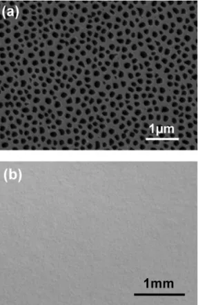
The NPSi was prepared by the AAO process and ICP technique on a 2 in. Si 共111兲 wafer. The anodization was performed at 6 ° C in 0.3 M phosphoric acid under an ap-plied voltage of 120 V. After anodization for 30 min, self-assembled AAO nanoarrays were uniformly distributed on the Si surface. By ICP etching, the AAO pattern was trans-ferred to the Si substrate. The AAO mask was then removed by wet etching. The top-view scanning electron microscope 共SEM兲 image in Fig.1共a兲shows the NPSi after removing the AAO mask. Nanopore arrays were uniformly distributed on the entire 2 in. Si substrate with an average nanopore diam-eter of ⬃150 nm, interpore distance of ⬃120 nm, and an etched depth of ⬃250 nm. LED structures were grown by metal-organic chemical vapor deposition in an Aixtron 2000 HT system. For comparison, the same LED structures were also grown on the MPSi 共340⫻340 m2grid-pattern sepa-rated by 20 m trenches兲. Detailed substrate preparation and growth procedure for LED on MPSi were reported elsewhere.13For the growth on NPSi, prior to the deposition, substrates were heated up to 1170 ° C for 10 min under H2
ambient to remove the native oxide on the surfaces. Then, an AlN nucleation layer共⬃40 nm兲 was deposited, followed by the growth of a 200 nm thick AlGaN buffer layer and an 800 nm thick undoped GaN. Before the growth of a 1 m thick Si doped GaN layer for contact, the 250 nm AlGaN/AlN interlayer which aimed to decrease the tensile stress was in-serted. Five stacks of InGaN/GaN multiple quantum wells
a兲Authors to whom correspondence should be addressed. Electronic
ad-dresses: [email protected] and [email protected]. Tel.: 852-23588843 and 852-23587049.
APPLIED PHYSICS LETTERS 96, 201106共2010兲
0003-6951/2010/96共20兲/201106/3/$30.00 96, 201106-1 © 2010 American Institute of Physics
This article is copyrighted as indicated in the article. Reuse of AIP content is subject to the terms at: http://scitation.aip.org/termsconditions. Downloaded to IP: 140.113.38.11 On: Wed, 30 Apr 2014 10:21:14
共MQWs兲 with well thickness of 2.6 nm and barrier thickness of 10 nm were grown as the active layer, and on top of MQWs, a 150 nm thick Mg doped p-GaN layer was depos-ited. After growth, the sample surface was examined under optical microscopy 关Fig.1共b兲兴. No crack could be observed on the whole wafer, and the surface was mirrorlike.
For cross-sectional transmission electron microscopy 共TEM兲 studies, both MPSi and NPSi samples were prepared using conventional mechanical thinning followed by ion beam milling. All TEM analyses were carried out on a JEOL 2010F field-emission microscope operating at 200 keV. Figures2共a兲and2共b兲show the full phase view of LED struc-tures imaged using multibeam bright-field diffraction condi-tion near the具11¯ 00典 zone axis. Although threading disloca-tions 共TDs兲 were visible in both types of samples, fewer dislocations were observed in the NPSi sample 关Fig. 2共b兲兴 and fewer dislocations extend to the MQWs region as com-pared to the MPSi sample 关Fig.2共a兲兴. Figures2共c兲and2共d兲
are TEM images taken from the interface of the epilayer/ NPSi in the same region but under different diffraction con-ditions. Figure2共c兲was collected under multibeam dark-field diffraction condition near具11¯ 00典 zone axis while Fig.2共d兲 used a two-beam dark-field under g =具0002典. Careful com-parison of Fig. 2共c兲 and2共d兲 indicates that several disloca-tions disappeared when g =具0002典. It suggests that most dis-locations had a Burger’s vector of具11 2¯0典/3 thus they were “a-type” dislocations. Moreover, it is obvious that most of the TDs were restricted in the AlGaN layer. Some disloca-tions changed their direcdisloca-tions by bending at the AlGaN/GaN interface, while some dislocations annihilated or bent inside the AlGaN buffer layer directly over the holes. As a result, the density of TDs at the top surface was much lower.
To investigate the residual strain in the GaN films, Ra-man backscattering measurements were performed at room temperature. Figure 3 compares the Raman spectra of the LEDs on NPSi and on MPSi. It was reported that the Raman shift of E2共High兲 in stress-free GaN layer is around
567.2 cm−1.20 The E2共High兲 shift is 565.4 cm−1 and
564.5 cm−1, for samples on NPSi and on MPSi, respectively.
The deviation of the E2共High兲 peaks from the intrinsic
posi-tion indicates the release of residual tensile stress. For GaN, the E2共high兲 mode shifts linearly with stress in 2.9 cm−1/GPa for biaxial stress. The estimated tensile stress
in NPSi and MPSi are 0.62 GPa and 0.93 GPa, respectively. It is obvious that the LED grown on NPSi has less tensile strained than that on MPSi, although both in situ SiNx and selective area growth technique were used during the growth of LED on MPSi. The stress difference is possibly due to the fact that when the patterns were in nanoscale, the initially formed GaN islands had relatively small size and narrow spacing. This would lead to a faster coalescence, and the coalescence boundary could facilitate the stress release.
FIG. 1. 共a兲 The top-view SEM image of the NPSi. 共b兲 The optical micro-scopy image of the surface of LED grown on NPSi.
FIG. 2. Bright-field images of LEDs grown on MPSi共a兲 and NPSi 共b兲, 共c兲 Multibeam dark-field images collected near zone axis.共d兲 Two-beam dark-field images collected using g =具0002典. Note that 共c兲 and 共d兲 are collected at the same region.
FIG. 3. Raman spectra of LEDs grown on NPSi and MPSi under z共xx兲z−
back scattering geometry.
201106-2 Deng et al. Appl. Phys. Lett. 96, 201106共2010兲
This article is copyrighted as indicated in the article. Reuse of AIP content is subject to the terms at: http://scitation.aip.org/termsconditions. Downloaded to IP: 140.113.38.11 On: Wed, 30 Apr 2014 10:21:14
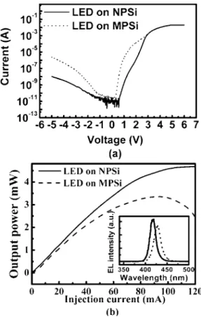
LED chips of 300⫻300 m2 were fabricated on both
NPSi and MPSi. Figure 4共a兲 shows the room temperature current-voltage 共I-V兲 characteristics of these two samples. Both types of LEDs exhibited a forward voltage of⬃4.7 V at 20 mA. The LEDs on NPSi exhibited a much lower leak-age current as compared to those on MPSi. This suggests that the density of TDs of the epitaxial film was reduced by using the NPSi. For the light output power measurement, the fab-ricated LED devices were mounted onto TO-5 cans. An in-tegrating sphere was used for collecting all the light emitted by the LED and directing the light to a charge-coupled de-vice detector. During the measurement, a Tektronix PS2520G programmable power supply was used to provide the biasing current. The current dependent output power共L-I兲 curves of these two unpackaged LED samples are shown in Fig.4共b兲. At the injection current of 20 mA, the output power of the LED on NPSi was 1.28 mW, 21% higher than that on MPSi. It should be noted that a slight portion of the power improve-ment may come from the 10 nm wavelength difference.21 Moreover, the output power of the LED on MPSi saturated at an injection current of⬃90 mA, while the output power of the LED on NPSi saturated at a higher current of⬃110 mA. The reduction in output power under high injection currents on the MPSi sample has been suggested to be related to TDs.22At high injection, phonon-assisted transport of holes via tunneling at defect sites along dislocation takes place, leading to an enhanced nonradiative parasitic process, thus, the output power is weakened. This is in good agreement with our observations in TEM. The inset of Fig.4共b兲shows the electroluminescence共EL兲 spectra of LEDs on NPSi and on MPSi at 20 mA injection current. An increase in intensity and a blueshift of the peak wavelength are noted on the NPSi sample as compared with the MPSi one. In combination with
the Raman results, the blueshift of the LED on NPSi is con-sidered as a sign of strain-release in the film grown on NPSi. In summary, crack-free InGaN based LED structures were grown and fabricated on NPSi. The material showed good surface morphology, reduced tensile strain, and lower dislocation density. The LEDs grown on NPSi exhibited a higher output power at 20 mA and a lower leakage current as compared with LEDs on conventional MPSi. These results suggest the feasibility of using NPSi for the growth of high power LEDs on Si substrates.
The authors wish to thank Tze Kin Cheung and Ching-Hsueh Chiu for useful discussions on this work. The research work was supported in part by a grant 共Grant No. 615705兲 from the Research Grants Council and a grant 共Grant No. GHP/034/07GD兲 from the Innovation and Technology Com-mission 共ITC兲 of Hong Kong Special Administrative Gov-ernment 共HKSAR兲.
1A. Dadgar, M. Poschenrieder, J. Bläsing, K. Fehse, A. Diez, and A. Krost,
Appl. Phys. Lett. 80, 3670共2002兲.
2S. A. Nikishin, N. N. Faleev, V. G. Antipov, S. Fancoeur, L. Grave de
Peralta, G. A. Seryogin, H. Temkin, T. I. Prokofyeve, M. Holtz, and S. N. G. Chu,Appl. Phys. Lett. 75, 2073共1999兲.
3H. Yu, M. K. Ozturk, S. Ozcelik, and E. Ozbay, J. Cryst. Growth 293, 273
共2006兲.
4S. Tanaka, Y. Honda, N. Sawaki, and M. Hibino,Appl. Phys. Lett.79, 955
共2001兲.
5E. Feltin, B. Beaumont, P. Vennéguès, M. Vaille, P. Gibart, T. Riemann, J.
Christen, L. Dobos, and B. Pécz,J. Appl. Phys. 93, 182共2003兲.
6M. Yamada, T. Mitani, Y. Narukawa, S. Shioji, I. Niki, S. Sonobe,
K. Deguchi, M. Sano, and T. Mukai,Jpn. J. Appl. Phys., Part 2 41, L1431
共2002兲.
7O. H. Nam, M. D. Bremser, B. L. Ward, R. J. Nemanich, and R. F. Davis,
Jpn. J. Appl. Phys., Part 2 36, L532共1997兲.
8A. Dadgar, M. Poschenrieder, J. Bläsing, O. Contreras, F. Bertram, T.
Riemann, A. Reiher, M. Kunze, I. Daumiller, A. Krtschil, A. Diez, A. Kaluza, A. Modlich, M. Kamp, J. Christen, F. A. Ponce, E. Kohn, and A. Krost,J. Cryst. Growth 248, 556共2003兲.
9S. D. Hersee, D. Zubia, X. Sun, R. Bommena, M. Fairchild, S. Zhang, D.
Burckel, A. Frauenglass, and S. R. J. Brueck,IEEE J. Quantum Electron. 38, 1017共2002兲.
10D. Zubia, S. H. Zaidi, S. D. Hersee, and S. R. J. Bruech,J. Vac. Sci.
Technol. B 18, 3514共2000兲.
11D. Zubia and S. D. Hersee,J. Appl. Phys. 85, 6492共1999兲.
12C. H. Chan, C. H. Hou, S. Z. Tseng, T. J. Chen, H. T. Chien, F. L. Hsiao,
C. C. Lee, Y. L. Tsai, and C. C. Chen, Appl. Phys. Lett. 95, 011110
共2009兲.
13B. Zhang, H. Liang, Y. Wang, Z. Feng, K. W. Ng, and K. M. Lau,J. Cryst.
Growth 298, 725共2007兲.
14L. Macht, P. R. Hageman, S. Haffouz, and P. K. Larsen,Appl. Phys. Lett.
87, 131904共2005兲.
15K. Y. Zang, S. J. Chua, J. H. Teng, N. S. S. Ang, A. M. Yong, and S. Y.
Chow,Appl. Phys. Lett. 92, 243126共2008兲.
16K. Y. Zang, Y. D. Wang, S. J. Chua, and L. S. Wang,Appl. Phys. Lett. 87,
193106共2005兲.
17A. Y. Polyakov, A. V. Markov, M. V. Mezhennyi, A. V. Govorkov, V. F.
Pavlov, N. B. Smirnov, A. A. Donskov, L. I. D’yakonov, Y. P. Kozlova, S. S. Malakhov, T. G. Yugova, V. I. Osinsky, G. G. Gorokh, N. N. Lyahova, V. B. Mityukhlyaev, and S. J. Pearton, Appl. Phys. Lett. 94, 022114
共2009兲.
18J. Liang, S. K. Hong, N. Kouklin, R. Beresford, and J. M. Xu,Appl. Phys.
Lett. 83, 1752共2003兲.
19H. Masuda, H. Yamada, M. Satoh, H. Asoh, M. Nakao, and T. Tamamura,
Appl. Phys. Lett. 71, 2770共1997兲.
20F. Demangeot, J. Frandon, M. A. Renucci, O. Briot, B. Gil, and R. L.
Aulumbard,Solid State Commun. 100, 207共1996兲.
21A. Y. Kim, W. Götz, D. A. Steigerwald, J. J. Wierer, N. F. Gardner, J. Sun,
S. A. Stockman, P. S. Martin, M. R. Krames, R. S. Kern, and F. M. Steranka,Phys. Status Solidi A 188, 15共2001兲.
22B. Monemar and B. E. Sernelius,Appl. Phys. Lett. 91, 181103共2007兲.
FIG. 4. 共a兲 The I-V characteristics. 共b兲 The L-I curves. The inset is the comparison of EL spectra at 20 mA injection current.
201106-3 Deng et al. Appl. Phys. Lett. 96, 201106共2010兲
This article is copyrighted as indicated in the article. Reuse of AIP content is subject to the terms at: http://scitation.aip.org/termsconditions. Downloaded to IP: 140.113.38.11 On: Wed, 30 Apr 2014 10:21:14