A Generic Multi-Dimensional Scan-Control Scheme
for Test-Cost Reduction
CHIA-YI LINAND HUNG-MING CHEN Department of Electronics Engineering
National Chiao Tung University Hsinchu, 300 Taiwan
This paper proposes a generic multi-dimensional scan shift control concept for mul-tiple scan chain design. Mulmul-tiple scan chain test scheme provides very low scan power by skipping (selectively load/unload) many long scan chain switching activities. Based on the two-dimensional scan shift control, we can achieve low test power with simple and small overhead structure. We can further extend the scheme to a generic N dimension test scheme. The proposed scheme skips many unnecessary don’t care (X) patterns to reduce the test data volume and test time. The experimental results of the proposed 2-D scheme achieve significant improvement in shift power reduction, test volume and test time re-duction. Compared with traditional single scan chain design, the large benchmark b17 of ITC’99 has over 50% reduction in test data volume and over 40% reduction in test time with little area overhead, around 1% routing overhead, and the power reduction is over 97%.
Keywords: DFT, low power, scan chain, compression, test data volume
1. INTRODUCTION
Due to the increasing number of devices in one chip, the VLSI design faces a great challenge in the increasing test cost. Test power, test data volume and test time are all important issues in testing field. When the chip is in test mode, some test patterns acti-vate all the blocks inside the chip, which causes large power consumption and may dam-age the chip during test [1]. Another issue is test data volume. The memory capacity of ATE (Automatic Test Equipment) is limited but large test data volume forces the test company to upgrade the ATE, which is very costly. If the test time is reduced, the chip test process cost will also be reduced.
Ravikumar in [2] lists some power reduction techniques like scan cell reordering, scan chain segmentation, and scan chain disabling. In fact, multiple scan chain is a kind of scan chain segmentation and it can also be implemented as scan chain disabling tech-nique. Multiple scan chain has shorter sub-scan-chain length and that really reduces much scan shift power. [3, 4] use this kind of techniques to reduce test power. Researchers in [5] and [27] further reduce the scan pins by using multi-cast technique. In order to diminish the switching activities of the test pattern, minimum transition fill (MT-fill) in [6] is one of the low test power techniques. With the help of encoding technique, researchers in [7] apply Golomb coding to shrink the test data volume and transitions of the test pattern. Linear feedback shift register (LFSR) based technique is also a popular test architecture. By using extra registers and control signals, the embedded test pattern generator [8] can generate low power test pattern [9-11]. In order to disable the unnecessary switching
activities in a multiple-scan-chain scheme, [4] only deals with the necessary scan-in data and scan-out data. Furthermore, authors in [12] try to minimize the distance between scan- in data and scan-out data.
The test circuit complexity increases, so does the test data volume. Test pattern compression is one of the solutions to reduce the large test data volume. Various encod-ing techniques have been applied in this field. Huffman encodencod-ing, Golomb encodencod-ing, and 9 code encoding have been proposed and these techniques provide different compression results [13, 14]. Due to the large amount of X bits in test pattern, researches modify the test structure and manipulate the test pattern to reduce scan-in data [15, 16]. In addition, researchers in [17-19], and [26] use memory array concept to fill the test pattern into the scan flip-flops. This concept can also reduce test power, test data volume and test time at the same time. In test time reduction, researchers in [20, 21] apply bypass technique to test the multiple modules or segments in one chip to reduce scan-in time. Authors in [22, 23] calculate the X bit distribution in the test pattern to segment a long scan chain to multiple scan chain. The scan-in data passes through mux to the determined segment, which can reduce many scan-in cycles.
In this paper, we propose a generic multi-dimensional scan shift control idea for multiple scan chain design. We can fulfill the multiple scan chain control design and re-duce test power, test data volume and test time. The rest of this paper is organized as fol-lows. Section 2 presents the proposed 2-D scan architecture and the concept of our methodology. Section 3 presents the test data manipulation details and implementation flow. Section 4 presents the 3-D architecture. Section 5 shows the experimental results with ISCAS’89 and ITC’99 circuits. Section 6 discusses the limitation of the proposed scheme. Section 7 concludes this paper.
2. PROPOSED ARCHITECTURE
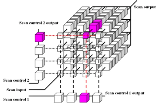
The proposed scheme uses memory block concept to design multiple scan chain. By using two-dimensional scan shift control as location indicator, each sub-scan-chain can operate independently in scan-in mode. Fig. 1 shows the proposed two-dimensional scheme.
Fig. 1. The proposed multiple scan chain architecture with 2-D 4 × 4 scan shift control chains. Combined with the proposed methodology, this test scheme can achieve low test power, small test data volume, and short test time with very little area overhead.
Scan control 1 and 2 indicate the sub-scan-chain location. When the location of the sub- scan-chain is determined, the specific test pattern is shifted from the scan input. While the scan-in operation is running, the scan-out data is shifted out from the scan output.
Since we need the scan-out data to check the correctness of the chip fabrication, we consider the scan-in test patterns and the scan-out patterns simultaneously when we en-code these test patterns. Because there are many X bits sequences inside the test pattern, we can use scan control to skip the scan-in and scan-out operations. With the help of scan control, the proposed scheme saves test power, test data volume, and test time si-multaneously.
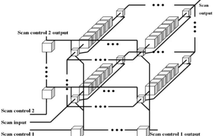
Fig. 2 shows the design details of the proposed scheme. The scan control 1 applies control signals to the control circuit of each sub-scan-chain in each column. The scan control 2 provides the row bank control signal. Fig. 3 reveals the control circuit design by logic gates. Scan control 1i in Fig. 3 (a) connects to the flip-flop signal 1i in Fig. 3 (b). Scan control 2 uses the same principle to connect to the control signals. From Figs. 2 and 3, we can perceive that the scan input signals will be masked if the control signal does not enable the sub-scan-chain.
Fig. 2. The design diagram of the proposed test architecture with routing connection details.
(a) (b)
Fig. 3. Circuit design of the proposed architecture; (a) shows the signal path of the sub-scan-chain design concept. The shift clock also needs to be activated or disabled during the scan op-eration; (b) presents the details for one scan control chain.
2.1 The Two Test Mode of the Proposed Scheme
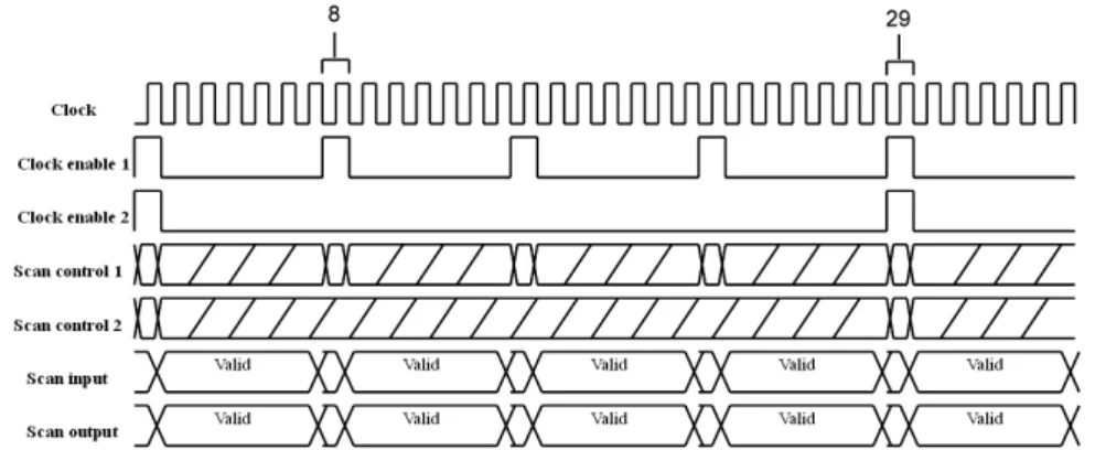
This scheme has two scan modes: regular scan mode and skipping scan mode. The regular scan mode shifts the test pattern from the first sub-scan-chain to the last sub- scan-chain in order. The skipping scan mode shifts the required sub-scan-chain patterns only. Fig. 4 shows the waveform of the behaviors of the control signals in regular scan mode. Fig. 5 shows the waveform of the behaviors of the control signals in skipping mode. In fact, we need to add 2 bits of control data to deliver the test patterns to the cor-rect sub-scan-chains. This way, we can reduce many unnecessary shifting operations in skipping scan mode. We use rising edge trigger as examples in Figs. 4 and 5. The scan control 1 and 2 need one clock to shift the scan control chain data when the clock enable 1 and 2 are activated.
Fig. 4. Regular scan mode waveform. In regular scan mode, the test patterns are shifted one seg-ment by one segseg-ment.
Fig. 5. Skipping scan mode waveform. The test patterns in skipping mode contain signal control codes which skip the segments with all X bits. In this figure, the 15th and the 16th cycles skip two segments of sub-scan-chains, which can reduce the test cost.
2.1.1 The working behavior of the regular scan mode
of the first flip-flop values in the scan control 1 and 2 are reset to 1 to indicate the scan-in data location. From Fig. 4, test data are shifted into the sub-scan-chain from the scan input during the next 6 cycles and the data inside the sub-scan-chain flip-flops are shifted out from the scan output. The scan control 1 shifts the value 1 from the first flip-flop to the second flip-flop to indicate the next sub-scan-chain at the 8th cycle. At the 29th cycle, the first flip-flop value of scan control 1 is set to 1 again and the first flip-flop value of scan control 2 is shifted to the second flip-flop. These regular opera-tions shift the test patterns into each of the sub-scan-chain.
2.1.2 The working behavior of the skipping scan mode
The skipping mode operation is shown in Fig. 5. The first flip-flop value of the scan control 1 and 2 is reset to 1. The operations of 15th and 16th cycles shift the flip-flop value of scan control 1 from the 2nd flip-flop to the 4th flip-flop. Due to the five succes-sive skipping control codes, this scheme skips 5 sub-scan-chains from the 23rd cycle to the 27th cycle. The first flip-flop of scan control 1 sets value to 1 and shifts the flip-flop value of scan control 2 from the first flip-flop to the second flip-flop at the 23rd cycle. The flip-flop value of scan control 1 shifts from the first flip-flop to the fourth flip-flop at the 24th, the 25th, and the 26th cycles. The first flip-flop of scan control 1 value sets to 1 and shifts the flip-flop value of scan control 2 from the second flip-flop to the third flip- flop at the 27th cycle. With these operations, the proposed architecture can skip a lot of unnecessary scan in data.
3. TWO-DIMENTIONAL SCAN SHIFT CONTROL OPTIMIZATION METHODOLOGY
This section will introduce the optimization methodology on test volume, test time, and test power for the proposed two-dimensional scheme. The methodology consists of scan control data definition, sub-scan-chain data segmentation, and scan-in data encoding. First, we define the codes to be added to the new test patterns. Second, we propose the guidelines to get the flip-flop numbers in each scan control design. Third, a heuristic en-coding method is applied to reduce test data volume. Finally, we recommend an imple-mentation flow to realize this test scheme.
3.1 Control Signal for Encoding
We define a 2-bit control signal coding method for the proposed scheme. The defi-nition of the control signal codes are listed below:
• Code 00: Regular scan signal • Code 01: Skipping one segment • Code 11: Skipping multiple segments
Fig. 6 shows the encoding example which adds extra control signals to the test pat-terns. The original test data size is 42 bits and the encoded test data size is 32 bits in this
Fig. 6. An encoding example of control signal. In this example, we consider scan-in and scan-out data simultaneously because the scan-out date need to be observed. The scan-in data should push the previous test results for observation. The original test data size is 42 bits in this example. By applying our encoding method, the scan-in test data is shrunk to 32 bits.
example. Both of the scan-in and scan-out data in the first and the second segments are all X bits. Because of the successive skipping operation, the first skipping code is 11 and the second skipping code is 01. The first two bits of each segment are control code. However, not all of the test patterns need to be encoded. If the encoded test pattern length is longer than the original test pattern length, the encoding is not necessary. In this example, we encode the original test data. We need a simple decoder to decode the two-bit control code to operate the scan control. Finally, we can shift the test data into the correct sub-scan- chain and shift out the previous test result.
3.2 Sub-Scan-Chain Data Design
The flip-flop number of scan control 1 (LSCN1) and 2 (LSCN2) are estimated from the
total scan chain length (LTSCL) in Eqs. (1) and (2). Designer can use the value as reference
and choose the approximate value as the implementation value. The length of sub-scan- chain (Lseg) is calculated by the Eq. (3).
3 1 SCN TSCL L ≈ L (1) 3 2 SCN TSCL L ≈ L (2) 1 2 ( ) seg TSCL SCN SCN L ≈ L ÷L ÷L (3)
The length of the sub-scan-chain segment is affected by the length of control 1 and 2. If we have long LSCN1 and LSCN2, we will have short Lseg and have more chance to get a
segment of test pattern with all X bits. However, the area overhead will be higher due to the long length of LSCN1 and LSCN2. Designer can choose the value around (or smaller than)
the reference value to implement the test architecture. 3.3 Scan-in Data Encoding
Since the definition of the control code and the approximate value of the scan con-trol 1 and 2 are determined, we need to apply the concon-trol code to the test pattern. The pattern will be assigned as skipping scan mode pattern if the encoded pattern is shorter than original one.
Fig. 7. The proposed test design flow. In order to integrate the proposed scheme design into the traditional design flow, we insert an extra stage after the scan chain synthesis.
Fig. 8. The test scheme for stacked 3-D IC. 3.4 Implementation Flow
In order to realize the proposed test scheme to the traditional design flow, we add an extra step to the design flow. The extra step inserts the two-dimensional scan control cir-cuits after the scan chain synthesis stage. The proposed design flow is shown in Fig. 7. In the insertion stage, we insert the proposed two-dimensional scan shift control circuits into the design. The extra codes consist of wires, flip-flops, and combinational logic gates.
4. THE 3-D ARCHITECTURE
We further extend the 3rd dimension of the proposed architecture. The circuit design shows in Fig. 8. In this scheme, we need 1 scan input pin and 3 scan control pins. Each block in Fig. 8 can be seen as a 2-D based scan design. The 3rd dimension needs extra logic gates to control the 2-D blocks. The routing complexity in 3-D architecture is higher than 2-D architecture.
From the view of shift power, the multiple scan chain technique reduces many un-necessary switching activities. The 1-D, 2-D and 3-D based scan design will have similar
shift power. From the view of test data volume and time, 3-D architecture needs one more bit than 2-D. That will cause a little overhead in test data volume and time.
The shift operation of the 3-D architecture is similar to the proposed 2-D scheme. Every sub-scan-chain is controlled by the 3 control pins. The test pattern is shifted in from the scan input pin and sub-scan-chain selection is controlled by the scan control chains. Since the 3-D scheme has one more control pins than the 2-D scheme. The control signal should be different but similar.
5. EXPERIMENTAL RESULTS
The experimental results on ISCAS’89 and ITC’99 benchmark circuits are provided in this section. The test patterns are generated by Synopsys TetraMAX [24]. The power estimation method is weighted transition metric (WTM) from [6] and the implementation technology is UMC’s 0.18um cell library. In order to get the power comparison results, we use the single scan chain test patterns and fill the X bits with 0’s to normalize our results. 5.1 The Results on Test Power, Volume and Time
The results including test power, test volume, and test time are shown in Table 1. The second column is the total number of test patterns (Nptn). The third column is the
pat-tern length (Lptn). The fourth, fifth, and sixth column are the number of flip-flops in scan
control 1 (Nc1), 2 (Nc2), and sub-scan-chain length (Lseg). Tnew, Vnew, and Pnew present
new test time, new test data volume, and new test power of the proposed scheme. New test time and new test data volume are normalized by the single scan chain design. TCy-clenew (cycle), Volnew (bit), and Pwrnew (sw) are total test cycles, new test data volume, and switching activities during shift-in and shift-out. New test power is normalized by the power of filling all X’s with 0’s. The test time calculation contains control cycles and data shift cycles.
The original test power is calculated by scan-in and scan-out power. Because the proposed scheme consists of extra control scan chains, the power of the proposed scheme includes switching activities of each sub-scan-chain and the extra control scan chains. Table 1 shows that the test power consumption (Pnew) in each circuit. For example, the
b17 circuit has 11 scan control flip-flops in scan control 1, 11 scan control flop-flops in scan control 2, and 12 scan flip-flops in each sub-scan-chain. Compared with the tradi-tional single scan chain design, the power consumption, test data volume, and test time with our test scheme are 1.1% (98.9% reduction), 46.5% (53.5% reduction), and 54.7% (45.3% reduction).
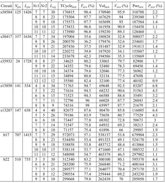
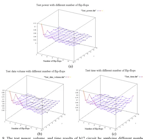
Table 1 shows the results of the same length of LSCN1 (the length of scan control 1) and LSCN2 (the length of scan control 2). We further calculate the test power, test data volume, and test time of the circuit b17 in different number of scan control flip-flops and present the results in Figs. 9 (a)-(c). Due to the various distributions of the X bits in the test patterns, different numbers of scan control flip-flops settings achieve different test power, test data volume, and test time reduction results.
From Table 1 and Fig. 9 (a), we can get a small power consumption result and a small test data volume result but the test time may not be the smallest one. Because large num-
Table 1. The experimental results show that the test power, test data volume and test time rate are reduced by applying small number of extra flip-flops in this scheme. Compared with traditional single scan chain and fill all X bits with 0’s, the proposed scheme provides low test power, small test data volume, and short test time, especially the large circuit (b17 or b22).
Circuit Nptn Lptn Nc1 Nc2 Lseg TCyclenew Tnew (%) Volnew Vnew (%) Pwrnew Pnew (%)
s38584 125 1426 7 7 30 176815 98.4 170940 95.9 310788 2.2 8 8 23 175504 97.7 167629 94 239380 1.7 9 9 18 175573 97.7 165698 93 187584 1.4 10 10 15 173833 96.8 161958 90.9 154458 1.1 11 11 12 173980 96.8 159230 89.3 128460 1 s38417 337 1636 7 7 34 197004 35.6 180828 32.8 308037 2.2 8 8 26 200370 36.2 179476 32.6 234601 1.7 9 9 21 207436 37.5 181487 32.9 191813 1.4 10 10 17 220272 39.8 187920 34.1 155887 1.2 11 11 14 233678 42.3 194586 35.3 135869 1 s35932 24 1728 8 8 27 34625 80.2 33065 79.7 82900 1.7 9 9 22 34352 79.6 32480 78.3 69450 1.4 10 10 18 34374 79.6 32046 77.3 56962 1.2 11 11 15 34894 80.8 32134 77.5 47698 1 12 12 12 35580 82.4 32100 77.4 40102 0.9 s15850 141 534 4 4 34 71763 94.7 69648 92.5 83207 6.8 5 5 22 71616 94.5 68232 90.6 51563 4.5 6 6 15 71523 94.3 66588 88.4 35491 3.2 7 7 11 72796 96 66028 87.7 26043 2.4 8 8 9 74316 98 65997 87.7 21679 2.1 s13207 147 638 4 4 40 82675 87.6 80470 85.8 116005 6.4 5 5 26 79186 83.9 75658 80.7 77529 4.3 6 6 18 73447 77.8 68302 72.8 50673 3 7 7 14 71547 75.8 64932 69.2 38213 2.4 8 8 10 71157 75.4 61896 66 29985 1.9 b17 707 1415 7 7 29 572073 57.1 538137 53.8 679904 2.3 8 8 23 534450 53.4 491323 49.1 524170 1.9 9 9 18 538858 53.8 483712 48.4 413066 1.5 10 10 15 538118 53.7 471660 47.1 388532 1.3 11 11 12 548098 54.7 465379 46.5 297902 1.1 b22 510 735 5 5 30 312340 83.2 300100 80.1 595370 4.4 6 6 21 285200 75.9 266840 71.2 408164 3.1 7 7 15 289577 77.1 264077 70.4 297170 2.3 8 8 12 290554 77.4 259444 69.2 243230 1.9 9 9 10 299668 79.8 262438 70 205050 1.7
ber of scan control may reduce the test data volume, the test time increases due to the long scan control time. In fact, Fig. 9 (b) shows that we can get the smallest test data volume with 10 flip-flops in scan control 1 and 9 flip-flops in scan control 2. The total extra scan flip-flop number is 19 and test data volume is 45.5%. Moreover, Fig. 9 (c) shows the shortest test time. With 10 flip-flops in scan control 1 and 9 flip-flops in scan control 2, the total test time is 51.6%.
(a)
(b) (c)
Fig. 9. The test power, volume, and time results of b17 circuit by applying different number of flip-flops in control 1 and 2. The x and y axes are horizontal. They represent the number of flip-flops in control 1 and control 2. The z axis is vertical, which represents the normalized value. This shows that different number of flip-flops in scan control 1 and 2 can get differ-ent results in test power, data volume, and time. And the prediction numbers from Eqs. (1)- (3) are reasonable and provide good results.
Table 2. Power and test data volume comparison.
Results in [11] Results in [9] Proposed results
Circuit Compression (%) reduction (%)Power Compression (%) reduction (%)Power Compression (%) reduction (%) Power
s13207 94 25 94 53 34 98.9
s15850 90 25 93 52 12.3 97.9
s38417 92 25 95 52 64.7 99
s38584 94 25 93 40 9.7 99
Table 2 shows the power and test data volume comparison with previous works. We compare the result with test data reduction rate (Compression (%)) and power reduction rate (Power reduction (%)). The proposed scheme does not reduce as much test data vol- ume in [9, 11]. However, the proposed scheme gets very power consumption.
5.2 The Realization of the Test Design
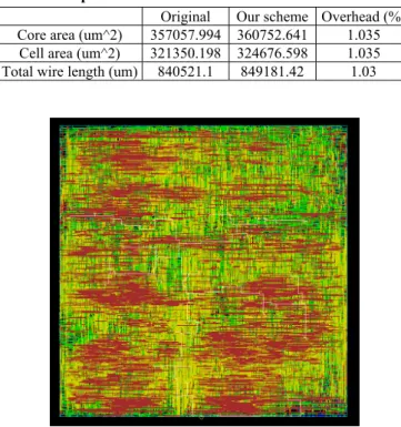
We use Cadence SOC Encounter [25] as placement and routing tool to implement the ITC’99 b17 circuit. The setting of aspect ratio is 1 and the core utilization is 0.9. With 8 flip-flops in scan control 1 and 8 flip-flops in scan control 2, we get 849181um in total length after detail route. Compared with the traditional one scan chain design, we have 1% extra routing overhead. We also provide the area and wire length results in Table 3. The first column is the traditional single scan chain design results (Original). The second column is our test scheme results (Our scheme). And the third column is the overhead results. The core area overhead, cell area overhead, and routing overhead are all around 1%. The routing result image of b17 circuit is shown in Fig. 10.
Table 3. The implementation overhead results of ITC’99 b17 circuit. Original Our scheme Overhead (%) Core area (um^2) 357057.994 360752.641 1.035
Cell area (um^2) 321350.198 324676.598 1.035 Total wire length (um) 840521.1 849181.42 1.03
Fig. 10. The routing result image of b17 circuit. The white lines are the scan-in paths. 6. DISCUSSION
With the 3rd dimension of scan control, the original 2-D scheme is independent in each stacked IC. We can use the 3rd dimension scan control to test each stacked IC inde-pendently. If we have the same sub-scan-chain number in each stacked IC, we can save data volume to record the difference of each stacked IC. However, if the sub-scan-chain numbers are different in each stacked IC, we need to record the difference in the test pattern file. We do not consider the ATE which can only perform fixed length and fixed cycle test to each test pattern in this paper, that is one of our work’s limitation.
Although the proposed scheme is similar to random access schemes, the proposed schemes focus on the smaller area overhead. Because the random access schemes use hardware decoders to access each scan flip-flop directly, the test time and test power in random access schemes might have better performance than the proposed schemes. The proposed schemes are tradeoff solutions.
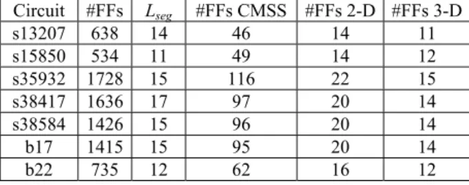
6.1 1-D vs. 2-D vs. 3-D Multiple Scan Chains in Area Overhead
In multiple scan chain schemes, we can use one control chain to deal with these sub-scan chains. We can call this kind of scheme as one-dimensional (1-D) scheme. Compared with the conventional 1-D scan control multiple scan chain scheme, Table 4 provides the comparison results. Although one-dimensional scan control multiple scan chain schemes also provide small shift-in power, the proposed two-dimensional scan control scheme has fewer control flip-flops than one-dimensional scan control scheme. In order to provide fair comparison, the results of Table 4 apply the same sub-scan-chain length (Lseg) in these two multiple scan chain schemes. The fourth column is the total
number of extra flip-flops of the conventional one dimension multiple scan chain in scan control 1 (#FFs CMSS). The fifth column is the total number of extra flip-flops in scan control 1 and 2 of the proposed 2-D test scheme (#FFs 2-D). The last column of Table 4 shows the extra flip-flops in scan control 1, 2 and 3 in the 3-D test scheme (#FFs 3-D).
Table 4. The overhead comparison with conventional one-dimensional multiple scan shift scheme. The proposed 2-D and 3-D scheme have significant reduction in the number of scan control flip-flops.
Circuit #FFs Lseg #FFs CMSS #FFs 2-D #FFs 3-D s13207 638 14 46 14 11 s15850 534 11 49 14 12 s35932 1728 15 116 22 15 s38417 1636 17 97 20 14 s38584 1426 15 96 20 14 b17 1415 15 95 20 14 b22 735 12 62 16 12
6.2 Multi-Dimensional Scan-Control Scheme Overhead Analysis
We have discussed about 2-D and 3-D scheme. In this section, we generalize the scan control length to Lscn (Lscn1, Lscn2, …, Lscnm) as Eq. (4). The assumption is that each
scan control dimension has the same number of flip-flops. The general overhead equa-tion of m multi-dimension scheme is shown in Eq. (5). Numff is the total number of
flip-flops in Eq. (5). In order to get an integer number of the Lscn, we can get the ceiling of
the value (⎡Lscn⎤) but the length of each scan control dimension should be adjusted at the
same time. Fig. 11 shows the Lscn and extra flip-flops of the generic scheme. From Fig. 11,
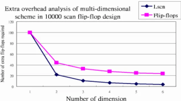
we can see that the extra number of flip-flops decreases very fast between 1-D and 2-D and the overhead of flip-flop number between 3-D to 6-D almost the same. However, the control signal routing overhead has not considered in this analysis. In recent design, we recommend 2-D or 3-D to implement this test scheme because high dimension may cause
Fig. 11. Extra overhead analysis of multi-dimensional scheme. The horizontal axis is the number of dimension. The vertical axis is the overhead. We use a 10000 scan flip-flops design as ex- ample to demonstrate the results.
heavy routing overhead. 1 m scn TSCL L ≈ + L (4) ff scn Num ≈m L× (5) 7. CONCLUSION
In this paper, we propose a multi-dimensional scan shift control test scheme to re-duce test power, test data volume, and test time with small area overhead. The results show that the power reduction in each benchmark circuit is significant in the 2-D test scheme. The test data volume and test time in each circuit are also improved in each cir-cuit. The circuit area overhead of the 2-D scan shift control scheme is better than the conventional one dimension scan control multiple scan chain scheme. Due to the simple control technique, the proposed 2-D scheme only has a little area overhead than tradi-tional single scan chain design in area and routing. The improvement of large circuits is especially significant, which indicates that the proposed scheme can scale to large circuit designs. We further extend this concept from 2-D to 3-D and compare the overhead of these test schemes. We recommend 2-D or 3-D test scheme to implement in the design with 10000 DFFs because high dimension of controls may cause routing overhead. How-ever, the gain is decreased in high dimension schemes. Finally, we provide the estima-tion Eqs. (4) and (5) as reference index in implementing this kind of test scheme.
REFERENCES
1. P. Girard, “Survey of low-power testing of VLSI circuit,” IEEE Design and Test of
Computers, Vol. 19, 2002, pp. 82-92.
2. C. P. Ravikumar, M. Hirech, and X. Wen, “Test strategies for low power devices,”
Design Automation and Test in Europe, 2008, pp. 728-733.
3. I. Lee, Y. M. Hur, and T. Ambler, “The efficient multiple scan chain architecture reducing power dissipation and test time,” in Proceedings of the 13th Asian Test
Symposium, 2004, pp. 94-97.
4. M. Elm, H. J. Wunderlich, M. E. Imhof, C. G. Zoellin, J. Leenstra, and N. Maeding, “Scan chain clustering for test power reduction,” in Proceedings of the 45th Annual
Design Automation Conference, 2008, pp. 828-833.
5. K. J. Lee, J. J. Chen, and C. H. Huang, “Using a single input to support multiple scan chains,” in Proceedings of International Conference on Computer-Aided
De-sign, 1998, pp. 74-78.
6. R. Sankaralingam, R. R. Oruganti, and N. A. Touba, “Static compaction techniques to control scan vector power dissipation,” in Proceedings of the 18th IEEE VLSI
Test Symposium, 2000, pp. 35-40.
7. A. Chandra and K. Chakrabarty, “Low-power scan testing and test data compression for system-on-a-chip,” IEEE Transactions on Computer-Aided Design of Integrated
Circuits and Systems, Vol. 21, 2002, pp. 597-604.
8. J. Rajski, J. Tyszer, M. Kassab, and N. Mukherjee, “Embedded deterministic test,”
IEEE Transactions on Computer-Aided Design of Integrated Circuits and Systems,
Vol. 23, 2004, pp. 776-792.
9. J. Lee and N. A. Touba, “LFSR-reseeding scheme achieving low-power dissipation during test,” IEEE Transactions on Computer-Aided Design of Integrated Circuits
and Systems, Vol. 26, 2007, pp. 396-401.
10. G. Mrugalski, J. Rajski, D. Czysz, and J. Tyszer, “New test data decompressor for low power applications,” in Proceedings of ACM/IEEE Design Automation
Confer-ence, 2007, pp. 539-544.
11. P. M. Rosinger, B. M. Al-Hashimi, and N. Nicolici, “Low power mixedmode BIST based on mask pattern generation using dual LFSR reseeding,” in Proceedings of
International Conference on Computer Design, 2002, pp. 474-479.
12. J. Li, Q. Xu, Y. Hu, and X. Li, “On reducing both shift and capture power for scan- based testing,” in Proceedings of ACM/IEEE Asia and South Pacific Design
Auto-mation Conference, 2008, pp. 653-658.
13. A. Chandra and K. Chakrabarty, “A unified approach to reduce soc test data volume, scan power and testing time,” IEEE Transactions on Computer-Aided Design of
In-tegrated Circuits and Systems, Vol. 22, 2003, pp. 352-362.
14. M. Nourani, M. Tehranipour, and K. Chakrabarty, “Nine-coded compression tech-nique with application to reduced pin-count testing and flexible on-chip decompres-sion,” in Proceedings of Design, Automation and Test in Europe Conference in
Ex-hibition, 2004, pp. 1284-1289.
15. H. Tang, S. M. Reddy, and I. Pomeranz, “On reducing test data volume and test ap-plication time for multiple scan chain designs,” in Proceedings of IEEE
Interna-tional Test Conference, 2003, pp. 1079-1088.
16. C. Y. Lin and H. M. Chen, “A selective pattern-compression scheme for power and test-data reduction,” in Proceedings of International Conference on Computer-Aided
Design, 2007, pp. 520-525.
17. H. Ando, “Testing VLSI with random access scan,” in Proceedings of Digest of Com-
puter Society International Conference, 1980, pp. 50-52.
18. D. H. Baik and K. K. Saluja, “Progress random access scan: A simultaneous solution to test power, test data volume and test time,” in Proceedings of IEEE International
19. Y. Hu, X. Fu, X. Fan, and H. Fujiwara, “Localized random access scan: towards low area and routing overhead,” in Proceedings of ACM/IEEE Asia and South Pacific
Design Automation Conference, 2008, pp. 565-570.
20. J. Aerts and E. J. Marinissen, “Scan chain design for test time reduction in core-based ICs,” in Proceedings of IEEE International Test Conference, 1998, pp. 448-457. 21. Z. Zhang, S. M. Reddy, I. Pomeranz, J. Rajski, and M. Al-Hashimi, “Enhancing
de-lay fault coverage through low power segmented scan,” in Proceedings of the 11th
IEEE Europe Test Symposium, 2006, pp. 21-28.
22. I. Lee, J. H. Jeong, and T. Ambler, “Two efficient methods to reduce power and test-ing time,” in Proceedtest-ings of International Symposium on Low Power Electronics
and Design, 2005, pp. 167-172.
23. S. P. Morley and R. A. Marlett, “Selectable length partial scan: A method to reduce vector length,” in Proceedings of IEEE International Test Conference, 1991, pp. 385- 392.
24. Synopsys, “Tetramax,” Synopsys Inc. 25. Cadence, “Soc encounter,” Cadence Inc.
26. S. P. Lin, C. L. Lee, and J. E. Chen, “A cocktail approach on random access scan toward low power and high efficiency test,” in Proceedings of IEEE/ACM
Interna-tional Conference on Computer-Aided Design, 2005, pp. 94-99.
27. C. W. Tzeng and S. Y. Huang, “UMC-scan test methodology: Exploiting the maxi-mum freedom of multicasting,” IEEE Design and Test of Computers, Vol. 25, 2008, pp. 132-140.
Chia-Yi Lin (林佳毅) received a B.S. degree in the Indus-trial Technology Educational Department from National Kao- hsiung Normal University, Kaohsiung, Taiwan, in 1998 and his M.S. degree in the Information Management Department from National Sun Yat-sen University, Kaohsiung, Taiwan, in 2001. He received his Ph.D. degree in the Department of Electronics Engineering, National Chiao Tung University, Taiwan in 2010. He interests in low power test of digital circuit and physical de-sign method in VLSI.
Hung-Ming Chen (陳宏明) received the B.S. degree in Computer Science and Information Engineering from National Chiao Tung University, Hsinchu, Taiwan, in 1993, and the M.S. and the Ph.D. degrees in Computer Sciences from University of Texas at Austin, in 1998 and 2003, respectively. He is currently an Associate Professor with the Department of Electronics Engi-neering, National Chiao Tung University, Hsinchu, Taiwan. Dr. Chen has been a member of some technical program committees, including IEEE SOCC, ASP-DAC and VLSI-DAT. His research interests include EDA (nanometer physical design and design me- thodology), beyond die-integration, design and analysis of algo-