An Integrated Ouasi-Planar
Leaky-Wave Antenna
Guang-Jong
Chou and
Ching-KuangC.
Tzuang, Senior Member, IEEEAbstract-A new quasi-planar leaky-wave antenna is presented. It consists of microstrip line on one side of the substrate and uniplanar circuit on the other side placed in a partially opened waveguide. The leakage is produced by the excitation of the first higher order (odd) microstrip mode coupled electromagnetically through slotline on the opposite side of the substrate. Theoretic results based on rigorous Green’s impedance integral equation method show that the new microstrip-slotline-coupled leaky-wave antenna has broadband tuning range via structure parameters and is insensitive to microstrip line width variation. Measured relative power absorbed (RPA) results indicate that the useful frequency bandwidth agrees with what rigorous field theory predicts. The measured antenna radiation patterns also agree very well with approximate theoretic computations. Theory and experiments show that the proposed leaky-wave antenna can interface to feeding structure easily and directly, the new antenna may become good candidate for microwave and millimeter-wave integrated antenna design.
I. INTRODUCTION
NTEGRATED antenna incorporating printed circuit radiat- ing structures and active circuits had become an important element in advanced millimeter-wave and submillimeter-wave quasi-optical communication system design [ 11-[8]. Attentions had been focused on array antenna realized in printed circuit form and suitable for quasi-optical integration of millimeter- wave system producing functions such as imaging, power combining, beam scanning, etc. Various types of antenna are being used for these arrays, e.g., grid array for power combining [9], log-periodic antenna for subharmonic mixer [lo], patch-antenna quasi-optical oscillator [8], [ 111, coplanar wave (CPW)-fed twin-slots antennas active array [6], folded- slots antennas for amplifier array [7], and many others [1]-[SI. This paper reports some progress being made toward the millimeter-wave integrated antenna system employing the quasi-planar leaky-wave antenna technology. The microstrip realization of the planar leaky-wave antenna was successfully implemented by Menzel [ 121. Yet the underlying operational principles and physics were not well developed until Oliner and Lee reported that such microstrip antenna radiated in the form of leaky wave of the first higher order mode [13], [14]. Oliner exploited new approach for scanning arrays at millimeter wavelengths when fabrication difficulties became a
Manuscript received March 10, 1995; revised December 13, 1995. This work was supported by the National Science Council, Republic of China, under Grant NSC 83-0425-E-009-019, NSC 84-2623-D-009-008, and NSC 84-2623-D-009-006.
The authors are with Institute of Electrical Communication Engineering, Microelectronics and Information Systems Research Center, National Chiao
Tung University, No. 1001, Ta Hsueh Road, Hsinchu, Taiwan, ROC. Publisher Item Identifier S 0018-926X(96)04752-7.
X
‘ I
-b-
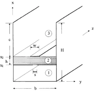
Fig. 1. antenna.
Geometry structure of the microstrip-slotline-coupled leaky-wave
serious problem [15]. A pencil beam can be derived and will scan in both elevation and azimuth (two-dimensional scanning) in a conical pattem by just incorporating a linear (one- dimensional) array of leaky-wave antennas. To accomplish the goal behind such approach for integrated active array antenna system, we propose and test a new leaky-wave antenna as shown in Fig. 1, which is quasi-planar in nature.
11. THE SUSPENDED MICROSTRIP-SLOTLINE-COUPLED LEAKY-WAVE ANTENNA
In Fig. 1. the unit-cell antenna consists of a microstrip line, a suspended slotline with two side planes of width nearly ( b - s ) / 2 connecting or not connecting the side walls of height
H , and a conductor-backed cavity of height XI. The guided
structure shown in Fig. 1 supports a dominant mode without dc cutoff, which was investigated thoroughly by Itoh [16] and regarded as a microstrip with tuning septum. This mode is even symmetric and should be avoided in our application. The first higher order mode is in odd symmetry and will leak in the form of the parallel-plate mode. Section I11 will discuss the full-wave analytical approach for obtaining the complex propagation constants that fully describe the leaky properties of the antenna. Extensive experiments and rigorous full-wave analyses have shown that the input reflection coefficient of the microstrip-slotline-coupled leaky-wave antenna fed by a slotline can be less than -20 dB [17]. This suggests that
CHOU AND TZUANG: AN INTEGRATED QUASI-PLANAR LEAKY-WAVE ANTEN
termination ,slotline
substrate
Fig. 2.
nar feed viewed upwardly from the cavity region @ of Fig. 1.
The microstrip-slotline-coupled leaky-wave antenna and the unipla
very effective interface to uniplanar microwave integrated circuits [IS] can be accomplished by the use of slotline. Fig. 2 shows one possible arrangement for the new integrated leaky-wave antenna. When viewed from the cavity-backed region
0
of Fig. 1 upwardly, the signals in CPW (coplanar waveguide) are converted into slotline forms which are then electromagnetically coupled to the microstrip line. Finally, the electromagnetic energy radiates into space as the waves propa- gate down the suspended microstrip-slotline-coupled structure. The leaky properties o f Fig. 1 will be discussed in Section IV, and the resultant antenna radiation pattern will be reported in Section V. We will discuss how to obtain the propagation characteristics of the leaky-wave antenna of Fig. 1 by rigorous full-wave approach in the following section.111. FULL-WAVE ANALYTICAL APPROACH BASED ON GREEN'S IMPEDANCE FUNCTION
The dispersion characteristics of the microstrip-slotline- coupled leaky-wave antenna are carried out by employing rigorous full-wave integral equation method using Green's impedance function approach. The unknowns in the integral equation are current distributions on the metal strips and are represented by a set of recently developed basis functions [ 191. When investigating a quasi-planar guided structure with a system of coupled conducting strips and slots, the Green's impedance function integral equation approach has shown advantages over conventional integral equation methods in the presence of nonlayered substrates. The longitudinal complex wave number k , =
f l
- j a and the time-harmonics factor ofelWt are assumed throughout the analyses. Galerkin procedure is then applied to solve the integral equation for the unknown surface currents corresponding to a system of linear equation. What follows is a brief description of the Green's impedance function integral equation approach.
The electromagnetic field components in each homogeneous region of Fig. 1 are described by two Hertzian potentials according to
NA 1079
where
s
= 1,2,
3 designates the regions0,
a,
anda
respectively. Here,n?'
andfit)
are Hertzian potential of TM and TE modes in the layered region s. In each homogeneous region the TM-to-s and TE-to-r are used to describe the hybrid fields. Satisfying the boundary conditions at the conducting walls, the potential functions in regions(
l
J
@, and0
can be expressed as follows. In region0
In region
0
In region Q
where
k&m = E& -
( y ) z
- k: and k~ is free-space wave number.At the interface between two adjaceni layered regions, the continuity conditions for the tangential electric and magnetic field components are
( l ) (2)
Substituting (3)-(5) into (1) and (2) leads to the field components in each layered region. Followed by applying
E(")
=v
xv
xnp)
- j w p v xnf)
the appropriate boundary conditions given in (7) at interface
IC = I C ~ and z = 2 2 , respectively, the relations between the coefficients
A%h,
B,“;$m,C;;im,
DZh,
and current distributionJ;“’
,
J;”’
can be obtained. By using the biorthogonal condition and eliminating coefficients shown in (3)-(5), one may derive the coefficient matrix in terms of unknown current distribution on every conducting strip, namelywhere
and s = 1 and 2.
[ I ] is the associated current matrix that relates the unknown coefficients with current distributions. Thereby, the tangential electric field components at the interface of each adjacent region can be expressed in terms of current distributions by using the relation shown in (8). Then one can write
Integrating (10) along all the metal strips, the general dyadic Green’s impedance function can be obtained
where
Let the unknown current distributions J$”’ and
Jis’
be expressed in terms of a complete set of basis functions. Following the Galerkin procedure to solve (1 l), a system of homogenous linear equation can be obtained. The nontrivial solution for the unknown current coefficients can be found by equating the determinant to zero. The roots of the determinant are the desired complex wave numbers of the microstrip- slotline-coupled leaky-wave antenna.Iv. LEAKY-WAVE PROPERTIES OF THE
NEW ANTENNA A. Propagation Characteristics
Numerical and experimental evaluations have been con- ducted for an antenna using CuFlonTM
’
substrate (Polyflon Company) of E, = 2.1 and thickness h = 0.762 mm. TheCuFlonTM is a trademark of Polyflon Company.
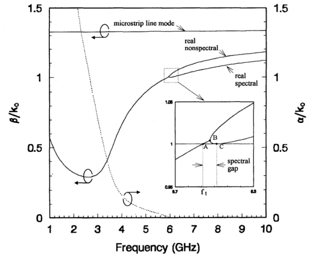
structure parameters are listed in Fig. 3, which plots the dominant mode (in even symmetry) and the first higher order mode (in odd symmetry) of this antenna. The dominant mode
is bound as expected whereas the first higher order mode leaks below approximately 6 GHz. Between 6 and 10 GHz, as indicated in Fig. 3, there are three real solutions, namely, the dominant mode, the real nonspectral solution, and the real spectral solution. The dominant mode is the microstrip mode perturbed by the slot in the ground plane and the solutions are nearly flat between 1 and 10 GHz. The real nonspectral solution is nonphysical and should be discarded. The real spectral solution is the first higher order mode of the microstrip line (or the slotline mode perturbed by the microstrip line by alternative back). In [20], a thorough discussion about the transition region of the partially dielectric-loaded open structure had been made. The dispersion characteristics of the first higher order mode of the microstrip-slotline-coupled leaky-wave antenna of Fig. 3 possess the similar leaky-wave propagation characteristics, as discussed in [20]. As frequency is reduced from 10 GHz, a transition region known as the spectral gap occurs over a frequency range defined between points A and C as shown in the inset of Fig. 3. The solutions in the spectral gap region are nonspectral and nonphysical.
These solutions are not captured by the steepest-descent path in the steepest descent plane [20]. Below the threshold point A, the complex solutions, although nonspectral, become captured by steepest-descent path and are therefore the physical leaky- wave solutions. Such complex propagation constant represents a forward leaky-wave radiating into the space at an angle Om
from broadside. The angle of maximum radiation (direction of the radiated beam) 8, is given by 8 , sin-’(P/ko).
B. Tunability and Sensitivity of the Leaky Wave Antenna
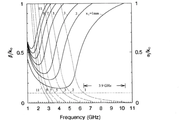
An important feature inherent in Fig. 1 is that the tunability of propagation characteristics can be fully understood by knowing k z and length L of the antenna. Therefore, the effect of changes of the structure parameters on leaky-wave prop- agation is analyzed before starting the design of leaky-wave antenna. What follows is based on the structure parameters given in Fig. 3. We change one structure variable each time. The variables include: 1) the cavity height 2 1 , 2) the antenna aperture b, 3) the slotline width s, and 4) the microstrip width
Fig. 4 illustrates the effect of cavity height z1 on the propagation characteristics of the leaky-wave antenna while keeping the rest of antenna parameters the same as those shown in Fig. 3. When the cavity height x1 is decreased from 11 to 1 mm the threshold frequency f t (defined in the inset of Fig. 3) moves from 3 to 10.3 GHz. This implies that at least two octaves of tuning spectrum are available for the particular design. For effective use of leaky-wave antenna, the normalized leakage (attenuation) constant a / k o
is usually kept below 0.1. Thus, we accept this assumption for defining the useful bandwidth of the leaky-wave antenna (as shown in Fig. 4) throughout the paper. Fig. 4 also reveals that the antenna useful bandwidth becomes broader by reducing W .
CHOU AND TZUANG: AN INTEGRATED QUASI-PLANAR LEAKY-WAVE ANTENNA 1081
1.5
1
0.5
Frequency
(GHz)
Fig. 3. .$ = 0.3 mm, h = 0.762 mm, c = 00, E,Z = 2.1 and ~~1 = ~~3 = 1.Dispersion characteristics of the microstrip-slotline-coupled leaky-wave antenna shown in Fig. 1, where 2 1 = 3 mm, b = 16 mm, w = 1.6 mm,
the cavity height XI. As a result the scan range within the useful bandwidth is larger with smaller cavity height z1 since the corresponding normalized phase constant /3/k0 has much greater variation. For example, when z1= 1 mm, the antenna
useful bandwidth is greater than 3.9 GHz and the value of the normalized phase constant /3/ko changes from 1 to 0.6. The corresponding antenna beam scans upwardly from horizon
(e,
= 90°, end-fire) at 10.3 GHz to 53'(0,
% 37") at 6.4 GHz approximately. When 2 1 = 2 mm, the useful bandwidth is about 2 GHz and the value of the /3/k0 varies from 1 to 0.73, resulting in 43" (0, E 47") antenna beam scanning as measured from horizon.The effect of aperture width b on the propagation charac- teristics of the leaky-wave antenna is shown in Fig. 5. The higher the value of aperture width b, the lower the threshold frequency f t is obtained. Such phenomena coincide with the fact that the cut off frequency of the parallel plate waveguide becomes smaller as the waveguide separation becomes larger. Similarly, when b is getting larger the threshold frequency becomes lower. It also shows that the wider aperture width results in wider useful bandwidth with steeper slope rate for
P / k O variation. It means that wider aperture results in more usable bandwidth and broader scan range, however, the beam direction Om will change more rapidly with frequency. The
choice of the aperture width b, however, is not arbitrary. In our case the aperture width is small enough so that the TM1 parallel-plate mode is avoided.
Fig. 6 shows the effect of the slotline width s on the prop- agation characteristics of the leaky-wave antenna. Although the curves of the normalized phase conlstant @ / k o and the normalized leakage constant a / k o in Figs. 5 and 6 are similar, the trend of the dispersion curves is different. It is observed that the larger the slotline width s, the stronger the effect of conductor back on the propagation Characteristics, resulting in the shift of threshold frequency ( f t ) moving toward higher frequency end. The significant effect of slotline width s on the propagation characteristics also makes it an important role for controlling the antenna leaky-wave properties.
The low sensitivity of the leaky-wave propagation char- acteristics with respect to the change of microstrip width w is illustrated in Fig. 7 for the particular case study. The dispersion curves for different microstrip width w show only a moderate change when microstrip line is widened by 80%
from original 1.0 mm width. The wider the microstrip is, the lower the threshold frequency will be.
Knowing the changes of leaky-wave antenna propagation characteristics with respect to the various structure parameter changes as shown in Figs. 4-7, a practical antenna design
1
0.5
0
1
0.5
0
1
2
3
4
5
6
7
8
9
1
0
1
1
Frequency
(GHz)
Fig. 4.leaky-wave antenna by changing cavity height 2 1 .
The normalized phase constant P / k o (solid line) and normalized leakage constant a / ko (dotted line) versus frequency of the microstrip-slotline-coupled
1
1
0.5
22
a
0.5
0
0
1
2
3
4
5
6
7
8
9
10
Frequency (GHz)
Fig. 5. The normalized phase constant p / k o (solid line) and normalized leakage constant a / k o (dotted line) versus frequency leaky-wave antenna change in aperture width b.
22
2
of the microstrip-slotline-coupled
may become possible. Notice that two to almost three octaves frequency variation can be achieved by using the initial structure parameters given in Fig. 3. When starting the leaky-
wave antenna design, we begin with certain assumed aperture width b, followed by the coarse tuning of leaky propagation characteristics by varying the cavity height 2 1 and slotline
CHOU AND TZUANG: AN INTEGRATED QUASI-PLANAR LEAKY-WAVE ANTENNA
1
9
2
0.5
0 10831
9
0.5
2
0
-
I
2
3
4
5
6
7
8
9
1
0
Frequency
(GHz)
Fig. 6 .leaky-wave antenna change in slotline spacing s.
The normalized phase constant P / k o (solid line) and normalized leakage constant a / k o (dotted line) versus frequency of the microstrip-slotline-coupled
1
0.5
0
1
0
1
2
3
4
5
8
7
8
9
1
0
Frequency (GHz)
Fig. 7.leaky-wave antenna change in microstrip width w .
The normalized phase constant ,!7/ ko (solid line) and normalized leakage constant a / k o (dotted line) versus frequency of the nicrostrip-slotline-coupled
width s. The fine tuning is performed by varying microstrip width w . After a few iterations, the leaky-wave antenna
design is completed with structure parameters in comfortable tolerance of photolithographic etching process.
63
P
.
8
2
-10r"
.- C cn -1 5 0.6 4 a E 0.4 0.2 -20 4 4.5 5 5.5 6 Frequencv(GHz)Fig. 8. Measured response and RPA of the microstrip-slotline-coupled leaky-wave antenna. L = 230 mm, H = 28 mm.
V. LEAKY-WAVE ANTENNA DESIGN
AND EXPERIMENTAL RESULTS
Based on the theoretical analyses outlined in Section IV, an experimental microstrip-slotline-coupled leaky-wave antenna was fabricated and tested. The dimensions of the experimental antenna were the same as that showed in Fig. 3 with side walls of height H = 28 mm and antenna length L = 230 mm. Thus, the propagation characteristics of the leaky-wave antenna are dictated by Fig. 3. The useful bandwidth is approximately between 4.5 GHz and 6 GHz. The efficiency and the input characteristics of the antenna were first observed by a two- port measurement. The complete leaky-wave antenna consists of a SO Cl CPW feed, CPW-to-slotline transition, slotline, the microstrip-slotline-coupled leaky (radiating) element, and termination, as shown in Fig. 2. We first conduct the rela- tive power absorbed (RPA) measurement on the leaky-wave antenna by not terminating the antenna but adding a second pair of identical CPW feed. Fig. 8 shows the results of the measurement. Between 4.7-5.0 GHz and 5.3-5.5 GHz, the VSWR's are less than 2.0 (ISl1(
<
-10 dB), showing that the well-matched condition is maintained. The leakage (radiation) efficiency of the antenna can be measured by the relative power absorbed (RPA) calculation, which is defined as 1-IS11I2- IS21I2 [21]. In Fig. 8 the experimental RPA results
show that there are two peak regions of efficiency greater than
80%, which imply that most energy leaks away. These two regions also coincide with the low VSWR region mentioned earlier. Nevertheless, greater than 60% efficiency is achieved throughout the useful bandwidth for the first-cut design. It should be noted that the conductor loss and the dielectric loss are not separated from the leakage power in the RPA calculation.
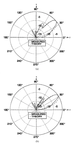
Next, we conduct the H-plane (the 2 - 2 plane) radiation
patterns measurement (in the anechoic chamber) at 4.6 and 5.05 GHz, respectively. The solid lines in parts (a) and (b) of Fig. 9 show the measured H-plane patterns at 4.6 and 5.05 GHz, respectively. By invoking the equivalent principle
X 4 90'
I/
300' 270' (b)Fig. 9. H-plane (;c-z plane) radiation patterns of the mi- crostrip-slotline-coupled leaky-wave antenna: (a) .f = 4.6 GHz. (b)
f = 5.05 GHz.
to the aperture surface and assuming that the fields outside the aperture are zero [22], we obtain the equivalent magnetic current distributions over the aperture surface written as
&!I = -2 x
Eaperature
for z E [0, L ] and y E [O, b] whereEaperture
= y E g e - j p z - o z andEo
is a constant.Notice that there is no field variation along y direction since the antenna leaks in the form of the parallel plate mode for the proper choice of aperture width b. Thus, the theoretical far-field radiation patterns can be derived from the Fourier transform over the aperture. The theoretic results are shown by broken lines in Fig. 9. Comparing the measured results and theoretic calculations, the beam angles agree to less than 1.5" difference and the measured beamwidths are a bit narrower than the theoretical patterns. The slight disagreement between theoretical and the experimental data may arise from ignoring the edge effect at the open ends of the antenna side walls.
1085 CHOU AND TZUANG AN INTEGRATED QUASI-PLANAR LEAKY-WAVE ANTENNA
VI. CONCLUSION
A quasi-planar leaky-wave antenna was proposed, analyzed,
built, and tested. Rigorous field-theory analyses of the new quasi-planar leaky-wave radiating element is presented. This results in useful design data that further explore the tunability and sensitivity of the new antenna and point to how to design the antenna in coarse and fine adjustment via the antenna structural dimensions. The measured RPA indicates that the useful bandwidth of the leaky-wave antenna does agree with the theoretic prediction for the antenna system including the discontinuity effect of all the transitions of the feeding structure. More than 80% antenna efficiency is achieved in the useful bandwidth band. Furthermore the measured and theoretic radiation patterns of the leaky-wave antenna are found to be in good agreement. Judging the fact that 1) the uniplanar feeding architecture of this antenna naturally adopts the active microwave circuits with ease and 2) the leaky-wave antenna is insensitive to the microstrip line width variation, the presented leaky-wave antenna design may become a good candidate for integrated antennas at microwave and millimeter- wave frequencies.
REFERENCES
K. Mizuno, Y. Daiku, and S. Ono, “Design of printed resonant antennas for monolithic-diode detectors,” IEEE Trans. Microwave Theory Tech.,
vol. MTT-25, pp. 470472, June 1977.
D. B. Rutledge and M. S. Muha, “Image antenna arrays,” ZEEE Trans. Antennas Propagat., vol. AP-30, pp. 535-540, July 1982.
D. P. Neikirk and D. B. Rutledge, “Self-heated thermocouples for far-infrared detection,” Appl. Phys. Lett., vol. 41, pp. 4 0 0 4 0 2 , Sept. 1982.
H. Kondo, M. Hieda, M. Nakayama, T. Tanakd, K. Osakahe, and K. Mizuno, “Millimeter and submillimeter wave quasi-optical oscillator with multi-elements,” ZEEE Trans. Microwave Theory Tech., vol. 40, pp. 857-863, May 1992.
G. M. Reheiz, D. P. Kasilingam, Y. Guo, P. A. Stimson, and D. B. Rutledge, “Monolithic millimeter-wave two-dimensional hom imaging arrays,” IEEE Trans. Antennas Propagat., vol. 38, pp. 1473-1482, Sept. 1990.
B. K. Kormanyos and G. M. Rebeiz, “20-GHz power combining slot-oscillator array,” IEEE Microwave Guide Wave Lett., vol. 4, pp. 226-228, July 1994.
H. S. Tsai, M. J. W. Rodwell, and R. A. York, “Planar amplifier array with improved bandwidth using folded-slots,” ZEEE Microwave Guide Wave Lett., vol. 4, pp. 112-114, Apr. 1994.
V. A. Thomas, K.-M. Ling, M. E. Jones, B. Toland, J. Lin, and T. Itoh, “FDTD analysis of an active antenna,” IEEE Microwave Guide Wave Lett., vol. 4, pp. 296-298, Sept. 1994.
W. A. Shiroma, B. L. Shaw, and Z. B. Popovic, “A 100-transistor quadruple grid oscillator,” IEEE Microwave Guide Wave Lett., vol. 4, T.-H. Lee, C.-Y. Chi, J. R. East, G. M. Reheiz, and G. I. Haddad, “A novel biased anti-parallel Schottky diode structure for subharmonic mixing,” IEEE Microwave Guide Wave Lett., vol. 4, pp. 341-343, Oct. 1994.
P. Liao and R. A. York, “A varactor-tuned patch oscillator for active arrays,” IEEE Microwave Guide Wave Lett., vol. 4, pp. 335-337, Oct. 1994.
W. Menzel, “A new travelling-wave antenna in microstrip,” Arch. Elek.
Uhertragung, vol. 33, pp. 137-140, Apr. 1979. pp. 350-351, Oct. 1994.
[I31 A. A. Oliner and K. S. Lee, “The nature of the leakage from higher modes on microstrip line,” in IEEE Int. Microwave Symp. Dig., Balti- more, MD, June 1986, pp. 57-60.
__, “Microstrip leaky wave strip antennas,” in IEEE Intl. Antennas Propag. Symp. Dig., 1986, Philadelphia, PA, June 1986, pp. 443-446. A. A. Oliner, “A new class of scannable millimeter-wave antennas,” in
Proc. 20th Eur. Microwave Con$, Budapest, Hungary, Sept. 1990, pp. T. Itoh, “Spectral domain immitance approach for dispersion character- istics of generalized printed transmission lines,” IEEE Trans. Microwave Theory Tech., vol. MTT-28, pp. 733-736, July 1980.
C.-K. C. Tzuang, G:J. Chou, and W.-T. Lo, “A. new quasi-planar leaky- wave antenna structure,” in 19th Znt. Con$ Infrared Millimeter Waves Dig., Seudai, Japan, Oct. 1994, pp. 518-519.
H. Ogawa, T. Hirota, and A. Minagawa, “Uniphndr MIC balanced multiplier-A proposal of new structure for MIC’s,” in IEEE Intl. Microwave Symp. Dig., Las Vegas, NV, May 1987, pp. 181-184. J.-W. Huang and C.-K. C. Tzuang, “Green’s impedance function ap- proach for propagation characteristics of generalized striplines and slotlines on nonlayered substrates,” IEEE Trans. Microwave Theory Tech., vol. 42, pp. 2317-2327, Dec. 1994.
P. Lampariello, F. Frezza, and A. A. Oliner, “The transition region between hound-wave and leaky-wave ranges .for a partially dielectric- loaded open guiding structure,” IEEE Trans. Microwave Theory Tech.,
vol. 38, pp. 1831-1836, Dec. 1990.
H. K. Smith and P. E. Mayes, “Log-periodic array of dual-feed mi- crostrip patch antennas,” ZEEE Trans. Antennas Propagat., vol. 39, pp. 1659-1664, Dec. 1991.
C. A. Balanis, Antenna Theory Analysis and De,rign. New York: Wiley, 1982, p. 533.
95-104.
Guang-Jong Chou was btaiii in Pong-Hu, Taiwan, on July 19, 1960 He received the B S E E degree from Chung Cheng Institute of Technology, Taiwan, in 1983, and the M.S. degree in communication engineering from National Chiao Tuang University, Hsinchu, Taiwan, in 1988. He is currently workmg toward the Ph.D. degree .it National Chiao Tuang University
From 1983 to 1993, he was with the Chung Shang Institute of Science and Technology, Lung-Tan, T a - wan, where he was involved in the design and maintenance of IFF system. His current research interests include mcrowave and mllimeter-wave integrated circuit design.
Ching-Kuang C. Tzuang (S’84-M’86-SM’92) was bom in Taiwan on May 10, 1955. He received the B.S. degree in electronic engineering from the National Chiao Tung University, Hsinchu, Taiwan, in 1977, the M.S. degree from the University of Califomia at Los Angeles, in 1980, and the Ph.D. degree in electrical engineering from the University of Texas at Austin, in 19136
From February 1981 to June 1984, he was with TRW, Redondo Beach, CA, worlung on analog and digital monolithic microwave integrated circuits While at the University of Texas at Austin, he workrd on high-speed translent analyses of monolithic mcrowave integrated circuits Since September 1986, he has been with the Institute of Communication Engineering, National Chiao Tung University, Hsinchu, Taiwan His research activities involve the design and development of rmlhmeter-wave and nucrowave active and passive circuits and the field theory analysis and design of various quasi-optical integrated antennas.