Electrical properties of shallow p + -n junction using boron-doped Si 1x Ge x layer
deposited by ultrahigh vacuum chemical molecular epitaxy
Hsiang-Jen Huang, Kun-Ming Chen, Chun-Yen Chang, Tien-Sheng Chao, and Tiao Yuan Huang
Citation: Journal of Applied Physics 89, 5133 (2001); doi: 10.1063/1.1321022
View online: http://dx.doi.org/10.1063/1.1321022
View Table of Contents: http://scitation.aip.org/content/aip/journal/jap/89/9?ver=pdfcov Published by the AIP Publishing
Articles you may be interested in
Ohmic contact properties of magnetron sputtered Ti 3 SiC 2 on n - and p -type 4H-silicon carbide Appl. Phys. Lett. 98, 042108 (2011); 10.1063/1.3549198
Rapid thermal annealing of ion beam synthesized - Fe Si 2 nanoparticles in Si Appl. Phys. Lett. 92, 211902 (2008); 10.1063/1.2936937
Comment on “Smooth relaxed Si 0.75 Ge 0.25 layers on Si ( 001 ) via in situ rapid thermal annealing” [Appl. Phys. Lett.83, 4321 (2003)]
Appl. Phys. Lett. 85, 5469 (2004); 10.1063/1.1828574
Analysis of the improved contact resistance in metal- p + silicon Schottky barriers using the BF 2 /B mixed implantation
Appl. Phys. Lett. 75, 1284 (1999); 10.1063/1.124669
Contacts on Si 1xy Ge x C y alloys: Electrical properties and thermal stability J. Vac. Sci. Technol. B 16, 1659 (1998); 10.1116/1.589848
Electrical properties of shallow
p
¿-
n
junction using boron-doped Si
1ÀxGe
xlayer deposited by ultrahigh vacuum chemical molecular epitaxy
Hsiang-Jen Huang, Kun-Ming Chen, Chun-Yen Chang,a)Tien-Sheng Chao, and Tiao Yuan Huang
Department of Electronics Engineering and Institute of Electronics, National Chiao-Tung University, Hsinchu 30050, Taiwan, Republic of China
共Received 16 March 2000; accepted for publication 5 September 2000兲
Strained boron-doped Si1⫺xGex layers with different Ge mole fractions were selectively deposited
by ultrahigh vacuum chemical molecular epitaxy to form shallow p⫹-n junction suitable for raised source/drain metal–oxide–semiconductor field effect transistor applications. Detailed electrical characterizations were performed. Our results show that the reverse leakage current could be optimized by a rapid thermal annealing at 950 °C for 20 s, and a near perfect forward ideality factor
共i.e., ⬍1.01兲 is obtained for the p⫹-n Si
1⫺xGex/Si junction. By analyzing the periphery and area
leakage current components of p⫹-n Si1⫺xGex/Si junctions with various perimeter lengths and areas, the degree of misfit dislocations and undercut effect were studied. The specific contact resistance was found to decrease as Ge mole fraction increases. Junction depth measurements also show that the junction depth decreases monotonically with increasing Ge mole fraction. The reduced B diffusion constant is attributed to the increasing Ge gradient in the transition region. © 2001
American Institute of Physics. 关DOI: 10.1063/1.1321022兴
I. INTRODUCTION
Heterojunction bipolar transistors with Si1⫺xGex bases
have been extensively studied in order to overcome the con-flicting requirements between base-resistance and transit-time limitation inherent in the conventional bipolar transistors.1–3In addition, the SiGe layer has also been pro-posed for forming the raised source/drain regions of metal– oxide–semiconductor共MOS兲 field-effect transistors, as well as for optical device applications.4,5 With a recent surge in research interest of the sub-0.1 m complementary MOS technologies, the issue of forming a shallow p⫹source/drain junction with low contact resistivity to minimize the short channel effects while maintaining the high current drivability has been highly researched. Unfortunately, the conventional ion implantation method has become increasingly difficult for forming the required shallow junction due to channeling and radiation damage. To overcome these problems, several methods have been proposed. Among them, the simplest and the most promising approach appears to be the use of an upper doped layer.6–11
The upper doped layer can be selectively deposited on the active region to form a shallow junction by several meth-ods including rapid thermal chemical vapor deposition
共RTCVD兲,12 and ultrahigh vacuum chemical molecular
epi-taxy 共UHVCME兲.7 For ultralarge-scale-integration applica-tions, however, it is crucial to minimize postdeposition dop-ant redistribution during subsequent thermal processes. Although this can be accomplished by reducing the subse-quent thermal budget, it usually places severe constraint on the subsequent process flexibility. Therefore, it would be
ad-vantageous to achieve minimum dopant redistribution by re-ducing the dopant diffusion constant. Previously, it has been pointed out that B diffusion from SiGe to Si is reduced in the SiGe/Si system due to the stress compensation effect.9,10 In addition, misfit dislocation density is lowered by using selec-tive epitaxial growth, compared to that of other large area deposition methods.13,14 The selective epitaxial growth
共SEG兲 feature is also advantageous in reducing the
undesir-able parasitic capacitance that often limits the transistor per-formance. Previously, the physical and electrical characteris-tics of selective SEG SiGe/Si diodes using RTCVD has been studied.15,16 The propagation of misfit dislocations was dis-cussed. Diodes fabricated in small deposited regions were shown to demonstrate more ideal forward characteristics than those fabricated in large regions. However, the effects of Ge ratio on the physical and electrical characteristics was not investigated.
The present article examines the structural and electrical properties of SEG Si1⫺xGex/Si p⫹-n heterojunction diodes
by using UHVCME-deposited Si1⫺xGexlayers with different
Ge mole fractions x on wafers containing oxide patterns. Besides being a low temperature process, UHVCME is also known to be advantageous in minimizing the impurity contamination due to its low base pressure. The electrical characteristics and dislocations caused by undercut effects and misfit at Si1⫺xGex/Si interface were studied in detail by
measuring diodes with various perimeter lengths and areas. A relative lower contact resistance is obtained with higher Ge composition in the Si1⫺xGex layer. Finally, the junction
depth reduction as a result of reduced B diffusion coefficient with increasing Ge composition is also discussed.
a兲Author to whom correspondence should be addressed; electronic mail: [email protected]
JOURNAL OF APPLIED PHYSICS VOLUME 89, NUMBER 9 1 MAY 2001
5133
0021-8979/2001/89(9)/5133/5/$18.00 © 2001 American Institute of Physics
II. EXPERIMENTS
n-type 6 in.共100兲 silicon wafers of 10–15 ⍀ cm
resis-tivity were used as the starting Si substrates. A 300 nm iso-lation oxide was first formed to define the active areas with various periphery and area ratios ( P/A). Then, following a standard RCA clean and a 1:50 HF:H2O dip, a 100 nm
B-doped Si1⫺xGex(x⫽0.09, 0.14, and 0.2兲 layer was
selec-tively deposited using the UHVCME system described previously.7Briefly, the growth chamber was pumped with a 1000 l/s turbomolecular pump to a standby base pressure of 2⫻10⫺10Torr. Wafers were first loaded into the loading chamber, and immediately transferred to the growth chamber for selective epitaxial growth. A base pressure of 1
⫻10⫺9Torr was routinely established within 1 min after the
wafer transfer process. Next, wafers were heated to the final deposition temperature of 550 °C at a ramp rate of⬃150 °C/ min. For growing the in situ B-doped Si1⫺xGex layer, pure
Si2H6, GeH4, and B2H6 were introduced into the growth
chamber. The chamber pressure was maintained below 1
⫻10⫺3Torr during epitaxial growth by the turbomolecular
pump. Then, a 200 nm tetraethylorthosilicate passivation ox-ide was deposited, which was followed by a rapid thermal anneal 共RTA兲 at various temperatures for dopant activation and outdiffusion. After contact opening, the TiN/Al–4%Cu/ TiN/Ti four-layer metal was then sputtered and patterned to form the metal interconnect. Finally, wafers were sintered in N2/H2at 400 °C before measurements.
The electrical characteristics were measured by a HP4145B semiconductor parameter analyzer. The sheet re-sistance was extracted using both the transmission length method共TLM兲17and cross-bridge resistor method, while the contact resistance was measured by both TLM and Kevin cross structures. Finally, the diffusion profile was measured by using secondary ion mass spectroscopy共SIMS兲 in a Cam-eca IMS5f apparatus. To obtain better accuracy, boron and oxygen profiles were obtained by using O2⫹ and Cs⫹, re-spectively, as the primary ion beams.
III. RESULTS AND DISCUSSION A. Electrical characteristics
Figure 1 shows the forward and reverse current–voltage characteristics of Si1⫺xGexdiodes with different Ge
compo-sitions. All samples were annealed at 950 °C for 20 s. It can be seen that the reverse leakage current increases only slightly with increasing Ge composition. However, the satu-ration current increases dramatically with increasing Ge ra-tio, i.e., the saturation current density JS is 63.8, 90.6, and
108.0 nA/cm2 for Si control, Si0.91Ge0.09, and
Si0.86Ge0.14SEG diodes, respectively. A larger JS for the
SiGe diodes with higher Ge composition is believed to be due to the increasing misfit dislocations caused by Ge atoms. In addition, at high current level, the Si0.86Ge0.14 diode also
depicts the highest forward current among the splits, indicat-ing a low contact resistance between metal and semiconduc-tor junction and therefore a lower effective series resistance. FIG. 1. The forward and reverse characteristics for SiGe/Si p⫹– n junction
with annealing at 950 °C for 20 s. The size of the diode area is 1000
⫻1000m2. The pure Si p⫹– n junction was made for comparison. The
epitaxial thickness of the SEG diodes is 100 nm.
FIG. 2. Forward ideality factor vs Ge composition with different RTA con-ditions. Solid line denotes RTA temperature at 950 °C for 20 s and dotted line RTA temperature at 900 °C for 30 s.
FIG. 3. The leakage current density JR vs P/A ratio of SEG Si1⫺xGex
diodes which were annealed at 950 °C for 20 s. JRis the reverse leakage
current density of the p⫹– n junction at⫺5 V.
5134 J. Appl. Phys., Vol. 89, No. 9, 1 May 2001 Huanget al.
It is also worth noting here that the Si0.91Ge0.09SEG diode depicts an ideality factor of better than 1.01 for over 7 de-cades.
The forward ideality factors versus Ge composition for different RTA conditions are plotted in Fig. 2. As Ge com-position increases, generally the ideality factor increases due to the increasing amount of misfit dislocations associated with more Ge atoms. For a sufficient RTA thermal budget
共e.g., 950 °C, 20 s兲, the measured junction depth is deeper
than 50 nm, and a near-perfect ideality factor is obtained. However, as the junction depth becomes shallower, such as the case for samples receiving RTA at 900 °C for 30 s with a junction depth of about 44 nm, the ideality factor increases slightly from 1.028 to 1.084 for the Si0.86Ge0.14diode. This is
because with a shallower junction, more Ge atoms would increase the amount of defects lying within the depletion region, giving nonideal behavior.
Figure 3 shows the plots of reverse leakage current den-sity JR versus the the P/A ratio for diodes with different Ge
compositions. All samples were annealed at the optimum RTA condition of 950 °C for 20 s. The reverse leakage cur-rent density was measured at ⫺5 V. By separating the re-verse leakage current density JR into the area component JA(nA/cm2) and the periphery component JP共nA/cm兲, and
by using the equation
JR⫽JA⫹共P/A兲JP, 共1兲
JA can be found by the intersection of the straight line with
the vertical axis, while JP can be found by the slope of the
straight line. The resultant JA and JP derived from these
curves are summarized in Fig. 4. It can be seen that JP
val-ues in a diode with a square or wide rectangular area are in general small and exhibit little change as Ge composition changes, suggesting the undercut effects along the isolation oxide edge during SEG process is reasonably small. In con-trast, JA values are relatively large and also increase with
increasing Ge composition. This is believed to be due to the FIG. 4. The calculated value of peripherial component of leakage current JP
and areal component JAvs Ge composition for SEG diodes after annealing
at 950 °C for 20 s. The solid line is JA, and dotted line is denoted JP.
FIG. 5. The calculated specific contact resistivity using both the TLM method and Kelvin resistor 共CBKR兲 method as a function of Ge mole fraction.
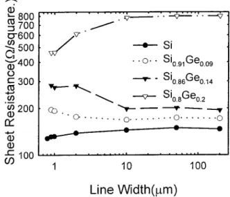
FIG. 6. Sheet resistance value vs linewidth of crossbridge resistors with different Ge mole fraction of Si1⫺xGexlayer deposited on the resistors.
FIG. 7. The sheet resistance value measured from both the TLM method and crossbridge resistors. The crossbridge resistors used here are 200m in linewidth.
5135 J. Appl. Phys., Vol. 89, No. 9, 1 May 2001 Huanget al.
severe extension of misfit dislocations formed at the Si1⫺xGex/Si interface.15 As a result, the areal leakage
rent constitutes a significant portion of the total leakage cur-rent, and degrades the reverse leakage performance. With increasing Ge composition, both the area and periphery leak-age currents increase. Increased Ge content atoms result in more severe misfit dislocations and defects along the inter-face region, and thus worsen the leakage current.
Measurement of specific contact resistivityC was
per-formed using both the TLM17and cross bridge Kelvin resis-tors. The results are summarized in Fig. 5. Only a small difference in specific contact resistivityC can be observed between the two methods. Theoretically, the barrier height
BPformed at the metal/semiconductor interface is known to
be a critical factor in determining the contact resistivityC.
It is known that the energy-band gap Egof Si1⫺xGexchanges
from 1.12 to 0.66 eV with increasing Ge mole fraction, and the conduction band edges are almost at the same level in metallurgical Si and SiGe junctions. However, the potential difference of the valence band will cause the lowering of the Schottky barrier height 共SBH兲 in metal/p⫹Si1⫺xGex
junction.18 For the pseudomorphic p-Si0.86Ge0.14 layer, the
SBH is expected to be lower than that of metal/ p⫹Si by 0.07 eV, which effectively reduces the specific contact resistivity
C. From Fig. 5, the specific contact resistivity indeed
de-creases as the Ge relative ratio changes from 0 to 0.14, as predicted. A minimum C value of 4.8⍀ cm
2
is observed for the Si0.86Ge0.14sample with low level in situ boron
con-centration of 1⫻1019cm⫺3 in the p⫹ region. However, the
C value jumps to a high value for a higher Ge ratio of 0.2.
This is believed to be due to severe dislocations at the Si0.8Ge0.2/Si interface.
To study misfit dislocations and dislocations formed by undercut effects in detail, the sheet resistance S of each sample was measured by crossbridge Kevin resistors. The measured sheet resistance as a function of linewidth for vari-ous samples is plotted in Fig. 6. For the Si SEG control sample, sheet resistance decreases as the resistor linewidth decreases and reaches a minimum value of 123⍀/䊐 for the Si control sample. This is because for a wider SEG area, the occurrence of dislocations and defects between the Si SEG region/Si substrate increases due to the propagation of misfit dislocation,15which leads to a higher sheet resistance value. On the contrary, for the Si0.91Ge0.09and Si0.86Ge0.14samples,
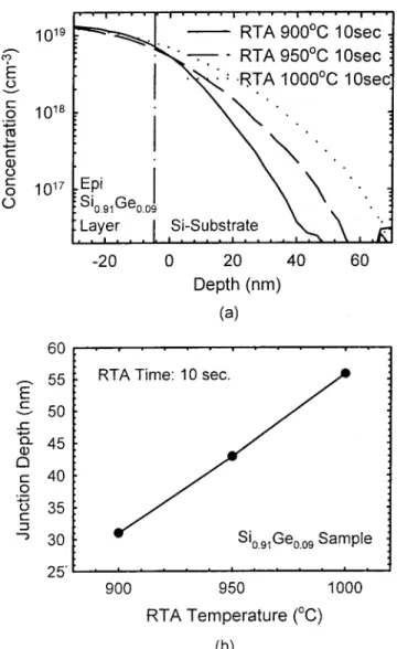
the sheet resistance increases as the linewidth decreases, due FIG. 8. 共a兲 SIMS boron profiles and 共b兲 junction depth vs Ge composition
for strained SEG Si and Si1⫺xGexlayer on Si substrate with annealing at
950 °C for 20 s.
FIG. 9. 共a兲 SIMS boron profiles and 共b兲 junction depth as a function of anneal temperatures for strained Si0.91Ge0.09layer on Si substrate with
an-nealing at various temperatures for 10 s.
5136 J. Appl. Phys., Vol. 89, No. 9, 1 May 2001 Huanget al.
to dislocations caused by undercut around the field oxide edge. The undesirable undercut effect is believed to be formed during the prebake process which is used for oxide removal prior to the selective epitaxy growth.16The prebak-ing temperature was kept at 1000 °C for 10 s. The boundary between substrate and patterned oxide can be attacked by such a preclean process. During subsequent selective epitax-ial deposition, the attacked region was partepitax-ially refilled. Cer-tain defects and dislocations were formed and nucleated at the edges of the oxide. This phenomenon is more apparent for the resistor with higher P/A ratio. Finally, for the Si0.8Ge0.2 sample, the sheet resistance decreases as the
line-width decreases. This is because for the sample with a high Ge ratio, the Si0.8Ge0.2/Si interface misfit dislocations in the
active region is much more severe than the undercut effects. The effects of Ge composition on the sheet resistance value are shown in Fig. 7. The sheet resistance was measured by both TLM and crossbridge resistors. It can be seen that both methods yield the same trend that with more Ge mole fraction in the SEG region, the value of sheet resistance be-comes higher, due to the increasing amount of misfit dislo-cations with more Ge atoms.
B. SIMS boron profiles and junction depth
Figure 8共a兲 shows the SIMS boron profiles of the SEG Si1⫺xGex structure with different Ge compositions. All
samples were annealed at 950 °C for 20 s. The B concentra-tion in the underlying Si substrate becomes lower with in-creasing Ge composition in the SEG region. Furthermore, the depth of the p⫹n junction is significantly reduced by
using the Si1⫺xGex/Si structure. In addition, all the B
pro-files, irrespective of Si or SiGe samples, are very similar to each other, indicating that the B diffusion constant in the SiGe layer is nearly identical to that in Si.8–10 On the other hand, from the previous studies, the decrease of boron diffu-sion coefficient occurs only at the Si1⫺xGex/Si interface
re-gion, which is the transition region from Si1⫺xGexto Si. By
increasing Ge composition in the SiGe layer, the Ge gradient in the transition region also increases, thus the effective B diffusion constant could be reduced. As a result, the reduc-tion of boron juncreduc-tion depth is effective when the juncreduc-tion depth is located in the underlying Si substrate. By defining the junction depth as the depth when the B concentration equals 2⫻1017cm⫺3, the junction depth value for all the
samples are summarized in Fig. 8共b兲. It can be seen clearly that the junction depth decreases monotonically as Ge com-position increases. Figure 9共a兲 shows the boron SIMS pro-files of the Si0.91Ge0.09sample after annealing at various
tem-peratures for 10 s. The calculated junction depths are plotted in Fig. 9共b兲. All the profiles are similar to each other. In addition, the incremental change of junction depth XJ is
slower than that of the pure Si sample, i.e., for the Si sample with RTA at 1000 °C for 10 s, XJ⫽62 nm; however, for the Si1⫺xGex sample at the same condition, XJ only equals
56 nm.
IV. CONCLUSION
The electrical characteristics of shallow p⫹/n diodes fabricated by selective epitaxial growth of the boron-doped Si1⫺xGex layer deposited by UHVCME were reported. It
was found that the reverse leakage current could be opti-mized by a RTA at 950 °C for 20 s with near ideal forward characteristics for the Si1⫺xGex diodes. The specific contact
resistance is found to improve with increasing Ge mole frac-tion. In addition, the junction depth decreases with increas-ing Ge composition, due to reduced B diffusion constant as a result of increasing Ge gradient in the transition region. However, due to the severe undercut effects along the local-ized oxidation of silicon field oxide edge during the SEG process, the periphery leakage current constitutes a signifi-cant portion of the total leakage current, and degrades the reverse leakage performance. The generalized information in this study should be useful for novel solid phase diffusion process and MOS field effect transistor applications.
ACKNOWLEDGMENTS
The authors would like to thank Dr. W. F. Wu and Dr. H. C. Lin for experimental assistance. This work was sup-ported in part by the National Science Council of the Repub-lic of China through Contract No. NSC89-2215-E009-050.
1X. Xiao, C. Sturm, S. R. Parihar, S. A. Lyon, D. Meyerhofer, S. Palfery, and F. V. Shallcross, IEEE Electron Device Lett. EDL-14, 199共1993兲. 2G. L. Patton, J. H. Comfort, B. S. Meyerson, E. F. Crabbe, B. De Fresart,
J. M. C. Stork, J. Y. C. Sun, D. L. Harame, and J. M. Burgatz, IEEE Electron Device Lett. EDL-11, 171共1990兲.
3J. M. Stork, E. J. Prinz, and C. W. Magee, IEEE Electron Device Lett. EDL-12, 303共1991兲.
4B. F. Levine, J. Appl. Phys. 74, R1共1993兲. 5
J. S. Park, R. P. G. Karunasiri, and K. L. Wang, Appl. Phys. Lett. 61, 681
共1992兲.
6T. F. Lei, T. P. Chen, H. C. Lin, and C. Y. Chang, IEEE Trans. Electron Devices 42, 2104共1995兲.
7
L. P. Chen, C. T. Chou, G. W. Huang, and C. Y. Chang, Appl. Phys. Lett. 67, 3001共1995兲.
8S. M. Hu, Phys. Rev. Lett. 63, 2492共1989兲.
9S. M. Hu, D. C. Ahlgren, P. A. Ronsheim, and J. O. Chu, Phys. Rev. Lett. 67, 1450共1991兲.
10
J. Sakano and S. Furukawa, Jpn. J. Appl. Phys., Part 1 32, 6163共1993兲. 11P. Kuo, J. L. Hoyt, J. F. Gibbons, J. E. Turner, R. D. Jacowits, and T. I.
Kanins, Appl. Phys. Lett. 62, 612共1993兲.
12D. T. Grider, M. C. O¨ ztu¨rk, S. P. Ashburn, J. J. Wortman, G. Harris, and D. Maher, J. Electron. Mater. 24, 1369共1995兲.
13
D. B. Noble, J. L. Hoyt, C. A. King, J. F. Gibbons, T. I. Kamins, and M. P. Scott, Appl. Phys. Lett. 56, 51共1990兲.
14E. A. Fitzgerald, Y.-H. Xie, D. Brasen, M. L. Green, J. Michel, P. E. Freeland, and B. E. Wier, J. Electron. Mater. 19, 949共1990兲.
15
T. I. Kamins, K. Nauka, R. D. Jacowitz, J. L. Hoyt, D. B. Noble, and J. F. Gibbons, IEEE Electron Device Lett. EDL-13, 177共1992兲.
16T. I. Kamins, K. Nauka, R. D. Jacowitz, J. L. Hoyt, D. B. Noble, and J. F. Gibbons, J. Electron. Mater. 21, 817共1992兲.
17H. H. Berger, Solid-State Electron. 15, 145共1972兲. 18
C. G. Van de Walle and R. Martin, Phys. Rev. B 34, 5621共1986兲. 5137
J. Appl. Phys., Vol. 89, No. 9, 1 May 2001 Huanget al.