國 立 交 通 大 學
應用化學系碩士班
碩 士 論 文
一維奈米結構釩氧化物VO
2,
V
2O
3和
β-Na
xV
2O
5之
成長及其鑑定
Growth of Characterization of Nearly-Aligned VO
2, V
2O
3and
β-Na
xV
2O
5Nanowires
研 究 生 : 柯智軒
指導教授 : 李積琛 博士
一維奈米結構釩氧化物VO
2,
V
2O
3和
β-Na
xV
2O
5之
成長及其鑑定
Growth of Characterization of Nearly-Aligned VO
2, V
2O
3and
β-Na
xV
2O
5Nanowires
研究生:柯智軒
Student : Jhih-Syuan Ke
指導教授: 李積琛 博士
Advisor : Chih-Shen Lee
國 立 交 通 大 學
應 用 化 學 系 碩 士 班
碩 士 論 文
A Thesis
Submitted to M. S. Program
Department of Applied Chemistry
College of Science
National Chiao Tung University
in Partial Fulfillment of the Requirements
for the Degree of Master of Science
in
Applied Chemistry
July 2011
Contents
Contents ... I
English Abstract ... III
Chinese Abstract ... V
Acknowledgements ... VII
List of Tables ... X
List of Figures ... XI
Chapter 1. Introduction ... 1
1.1 Brief review of 1D Nanomaterials ... 1
1.2 Family of Vanadium Oxide ... 3
1.2.1 Structure, Properties and Application ... 3
1.2.2 Literature Review of Vanadium Oxide ... 12
1.3 Ternary Phase of Bronze Vanadium Oxide
β
-Na
xV
2O
5... 14
1.3.1 Structure and Properties ... 14
1.3.2 Literature Review of
β
-Na
xV
2O
5... 16
1.3.3 Application ... 16
1.4 Thermal Evaporation-Like Synthesis for Vanadium Oxide NWs ... 18
1.5 Theory of Electron Field Emission ... 20
1.6 Aim of This Thesis ... 24
Chapter 2. Controlled Reduction of Nearly-Aligned Nanowires of V
2O
5to
VO
2(R), VO
2(B) and V
2O
3... 26
2.1 Introduction ... 26
2.2.1 Synthesis ... 27
2.2.2 Characterization ... 28
2.3 Results and Discussion ... 29
2.3.1 Synthesis and Reduction Condition ... 29
2.3.2 Structural and Purity Characterization ... 30
2.3.3 The Morphology and Structure of As-Obtained Typical Product 32
2.3.4 X-Ray Photoelectron Spectroscopic Analyses. ... 36
2.3.5 Transformation Mechanism ... 38
2.3.6 Electronic Field Emission Property. ... 40
2.4 Summary ... 42
Chapter 3 Controlled Synthesis of Nearly Vertical-Aligned Na
0.24V
2O
5Nanowire Thin Films ... 43
3.1 Introduction ... 43
3.2 Experimental Section ... 44
3.2.1 Synthesis ... 44
3.2.2 Characterization. ... 45
3.3 Results and Discussion ... 47
3.3.1 Structural and Composition Characterization ... 47
3.3.2 The Morphology and Structure of As-Obtained Monoclinic
Na
0.24V
2O
5NWs ... 48
3.3.3 X-Ray Photoelectron Spectroscopic Analyses ... 50
3.3.4 Optimization of Synthetic Condition ... 51
3.3.5 Formation Mechanism of As-Obtained Na
0.24V
2O
5NWs ... 54
3.3.6 Diffuse Reflectance Measurements ... 56
3.3.7 Electronic Field Emission Property. ... 58
3.4 Summary ... 60
Chapter 4 Conclusions ... 61
Growth of Characterization of Nearly-Aligned VO
2, V
2O
3and
β-Na
xV
2O
5Nanowires
Student: Jhih-Syuan Ke
Advisor: Dr. Chi-Shen Lee
M. S. Program, Department of Applied Chemistry
National Chiao Tung University
English Abstract
We report a deposition process to prepare nearly aligned binary and ternary vanadium oxides nanowires, including VO2(R), VO2(B), V2O3, and β-NaxV2O5. In the first section,
VO2(R), VO2(B), and V2O3 nanowires were prepared by reducing the precursor of V2O5
nanowires with controlled concentration of reducing gas flow and reduced period. The large portions of NWs microstructure are successfully preserved during the reduction, and are still nearly vertical-aligned on the surface. The growth directions of these reducing products were influenced by the growth direction of the original phase, V2O5 NWs. On the basis of the
growth direction of each product, possible mechanisms of conversion during reduction reaction are proposed. In the second section, β-NaxV2O5 nanowires were prepared via a route
combined the original thermal evaporation procedure with additive pre-treatment of the surfaces of substrates. The sodium silicate, source of the sodium, was first coated on the substrates and the amount of precursor was carefully controlled on a Na+-free substrate. The length of the β-Na V O wires could be controlled in the range of 5-25µm by changing the
reaction condition, which grew along the [100] direction.
X-ray powder diffraction (XRD) and transmission electron microscopy (TEM) were used to confirm the crystallinity of oxide nanowires. The effect of the controlled amount of deposited material and morphology were studied. A possible formation mechanism was proposed. The field emission properties of these binary and ternary vanadium oxides nanowires have been investigated. The results show that the as-prepared NWs possess excellent field emission performances with low turn-on field, large emission current density and linear Fowler-Nordheim behaviors. The studies suggest that these 1D nanomaterials could serve as promising candidates for future field emission devices.
一維奈米結構釩氧化物VO
2,
V
2O
3和
β-Na
xV
2O
5之
成長及其鑑定
學生: 柯智軒 指導教授: 李積琛 博士 國立交通大學應用化學系碩士班Chinese Abstract
在這份研究報告當中,我們提出一套新穎的合成方法來沉積接近垂直成長之奈米線 薄膜。能經由此套合成方法製備出的材料有R相之釩氧化二釩(VO2(R))、B相之二氧化釩 (VO2(B))、三氧化二釩(V2O3))以及β相的鈉釩氧化物(β-NaxV2O5)奈米線,這套合成方法 能細分成兩個部分。在第一部分當中,V2O5奈米線是作為一前驅產物,先一步的由熱 蒸鍍合成法製備而得。接著再進一步的將V2O5奈米線在還原氣體的氛圍下加熱,進行 還原反應。在此還原反應中,有影響的可變參數為還原溫度、還原反應時間以及還原氣 體的組成。經由準確的調控反應參數能夠成功的製備出三個具有不同結晶性釩氧化物的 奈米線,其中包括VO2(R),VO2(B)和 V2O3。在還原反應之後,獲得的釩氧化物能夠順 利得保有原先的奈米線構型,且奈米線也仍然是近乎垂直的排列在基板上。在研究奈米 線的結晶性的過程當中,我們發現被還原的釩氧化物其奈米線的成長方向會受到最原始 的V2O5奈米線的成長方向所影響。因此,在此論點的基礎下,我們考慮各個奈米線的 成長方向,成功的建構出在還原反應裡可能進行的轉變機制。 再另一個部分中,在原有的熱蒸鍍合成法中加入「基板前處理」後,β-NaxV2O5奈 米線就能成功的被製備獲得。在此系統中,矽酸鈉鹽是作為提供鈉離子來源的反應前驅 物,因此我們在不含鈉的基板上先一步的沉積一層矽酸鈉鹽薄膜並精準的控制其鈉的含 量。接著在熱蒸鍍合成法中,釩氧錯合物會被蒸氣攜帶至基板上再與基板上的鈉離子反 應,進一步的生成出β-NaxV2O5奈米線。經由X光粉末繞射與穿透式電子顯微鏡的量測 之後,能夠推測出β-NaxV2O5奈米線是沿著[100]的方向成長。在實驗的過程當中,我們 發現到會影響此反應的可變實驗參數有反應溫度,熱蒸鍍時所使用的釩氧離子溶液的濃度以及所使用的矽酸鈉鹽溶液的濃度。經由調控這些參數,能夠控制成長在基板上的奈 米線長度。最後在研究報告當中,我們將提出其可能的成長機制。
經由探討各個奈米線材的電子場發射性質,顯示出各個材料本身的性質與其場發射 特性具有相當的關連性。此報告中所製備出的奈米線皆具有低觸發電壓(turn-on field)、 高最大發射電流密度(emission current density)。製備出的奈米線材中,V2O3奈米線是有
較好的電子場發射性質,其觸發電場值為 5.2V/µm,而在電場值 8.3V/µm的作用底下所 測得的最大發射電流密度為 8.3mA/cm2。這些研究結果皆顯示出,釩氧化物奈米現在未
Acknowledgements
待在交大裡的時間算一算大概有兩千多個日子,六年的歲月真的很長,長到自己覺 得很膩、了無新意、很想離開,但是一旦到了要離開的日子,卻又感到分外的不捨,會 有這樣的惆悵情感應該不是我喜歡交大這所大學,而是我捨不得曾經有你們存在的交 大! 在這段歲月裡要感謝的人真的很多,首先我想要感謝的是我的老闆 李積琛老師, 老師在研究這條路上給予我很多的指導與幫助,而且認同我所做的實驗成果,冀望我能 夠投稿國外的學術期刊,對於這份信任我真的感到相當的開心、光榮然後是感謝。接著, 要感謝裘性天 老師以及孫建文 老師在百忙之中抽空來聆聽我的碩士研究成果報告,給 予我很多寶貴的建議以及能夠改進的地方,讓我的碩士論文的品質能夠更加提升。 充滿笑聲的實驗室生活也是讓人難以忘懷的,感謝在這實驗室內陪我一同奮鬥的好 夥伴們:實驗室的大長老-擁有處女座細膩、認真特質的呆呆,真的很感謝您!不論是 實驗、論文、生活上你都給予過我很多的幫助,真的感謝,每次去台中剪頭髮都少不了 你的陪伴,剪個頭髮都像是去台中出遊相當有趣,有機會再去找你玩吧!;很會照(ㄊ ㄧㄠˊ)顧(ㄎㄢˇ)學弟妹的阿明,欠你的十分鐘揶揄時間你到底要不要用掉呢?一 直欠著很難受耶 XD,前陣子還有一起相約去游泳的時候,在走去游泳的路上的談心時 間,感覺真的挺不賴的!從跟你的聊天當中我獲得很多,不僅僅是學術上、待人處事還 有一些有的沒的(你懂得!),如果我退伍後還沒閃光再一起去聯誼吧;總是充滿自信的 郝哥,感謝你在實驗上給我的建議,但是或許我能力不足,總是沒辦法順利的達成你給 的建議,另外也感謝你介紹我很多相當實用的東西,省去我不少爬文的時間;柔情鐵漢 的小 Ju,雖然你講的話很 A,但是真的都很好笑,沒有你的 A 笑話和超強的拳機火力 支援,我的碩一生活會黯淡不少;行動力超強的佳芬學姐,學姐的積極與作事的態度都 讓我相當的敬佩!妳超強的外語能力也讓我讚嘆不已,妳是我學習的楷模;酷愛 MLB 的家瑜學姐,在跟妳聊到 MLB 時,妳興奮的神情讓我相當的難忘,妳大概是我認識的 第一個會看 MLB 的女生吧;同學好幾年的陳拔剌,你真的很黑又很壯!強大的運動能 力讓我很羨慕 XD,其實我是個內向的小朋友,剛進實驗室的時候,你的存在讓我安心 不少,能夠和你一起熟悉這個陌生環境、成長茁壯到變成畢業學長姐,真的很開心也很 感謝!另外,也感謝你能讓我傾吐心事,變成真正的交心朋友,不過還是建議你可以再 八卦一點,這樣我說起故事來會比較賣力 XD;打桌球超帥的書維哥,你的幽默常常帶 給實驗室歡笑聲,你的心思細膩常常發現到我的不開心,能跟你和拔剌當同學真的很棒! 另外偷偷說,我常常把你當成我的目標,你的能力與認真的態度激勵我不少,你的存在 讓我的怠惰收斂許多,真的很感謝;一點都不黑而且很可愛的王允欣,果然叫妳還是要 叫全名感覺才對味呀!雖然你是個學妹,但妳是跟我們三個一起適應實驗室的好夥伴, 所以在我的認知裡妳一直都是跟我同屆吧,在這邊允許妳可以叫我柯智軒 XD!妳是個 貼心的好女孩,時常被妳的貼心舉動感動到,能夠變成妳的好姐妹、好哥們真的深感榮 幸!祝福妳;體魄愈來愈健壯的亞軍,你一直都是個嗨咖,在碩一的時候一直是大家揶 揄的對象,升上碩二之後,砲火好像少了很多!實在很可惜,沒辦法再看到你以一擋百的氣勢 XD,雖然跟你相識只有一年,但是跟你聊天都能很盡興;漸漸顯露本性的金魚, 最近常常聽到妳一針見血的尾刀真的很有趣!在重訓室見識到妳的 power,真的很不簡 單,看的我相當慚愧,我真的該好好努力鍛練一下了 XD;汗操很好的浩恩,你是個很 好揪的運動咖,跟你打羽球、桌球都很有意思,只可惜我的籃球很弱,沒辦法跟你打得 很盡興!另外你真的很愛垂坤的零食,有需要在摳我吧,隨時幫你訂;實驗室的新成員 VG、宅維、昀聲,跟你們相處的時間不長,但是感覺你們都是很有趣的人物,似乎都 很享受學長們的調侃 XD,真心希望你們會喜愛這個 CSlab,Enjoy it!;活潑可愛又很 sweet 的婉欣學妹,雖然妳常常說自己很不會安慰人,但是對我來說妳的關心就是一個 很好的慰藉。我們相差兩屆,沒辦法有更多的相處時光,真的感到相當的可惜,祝福妳 也能有個充實且愉快的兩年實驗室生活,Cheer up!。兩年的研究生生活因為有你們, 而變的精彩許多,真的很感謝大家!希望在未來還能夠有許多相聚的機會。 大學的四年生活也是讓我很感念的,即使我們大家已經經歷了一次離別,但兩年後 的今天再經歷一次,依舊相當捨不得,我的好朋友們:大軒、宏憲、冠達、楊立誠、小 明、百傑、阿伯、舜舜、拔剌、金毛、俊哥、李宥宗、小白、孔哥、大衛、stella、龔晏 瑩、琬妤、童思頻。我們之間的友情,或許已經無法用言語表達了,除了感恩、感謝也 想對你們說聲珍重再見。死黨級的高中朋友:小 a、小白沛昇、王蛋、阿鳥、月餅、黑 人邵、阿甘學妹、月餅妹,你們是我一輩子的朋友,每當我遇到挫折時的一個念頭就是 想要逃到你們身邊,你們的存在對我很重要,沒有你們就沒有現在的我,感謝;李大頭、 張阿嘎、賴冬瓜,雖然常常被妳們凹,但是我也樂在其中,你們都是好女孩,衷心希望 你們能夠順利找到自己的伴侶,如果不行,就等我開養老院養妳們好了 XD,另外我想 說的是,你們是我的好哥們!而不是好姐妹 XD。摯愛的高中老師,小橘老媽佩芳、帶 領我們的財哥、帥氣的堂智老師,高中這段日子對我的人生影響最大!主要的原因也是 有您們,財哥的領導風格我至今都很難忘懷,您的諄諄教誨讓我受益良多,我的個性有 一半都是你培養出來的,真的感謝;小橘老媽,能夠有個老師當我的乾媽真的是受寵若 驚,還記得畢業的時候在妳面前哭得半死不活的,那時的心情我真的難以忘記,每次妳 握著我的手跟我講道理,我真的感受到許多的溫暖。妳生了一個小女娃,變成了我的小 乾妹了,過去很忙還來不及去看我的小乾妹,一定是個可愛的圓臉女孩;堂智老師,你 當初帶領我們這隊去參加比賽,你的領導風格也是讓我很難忘記的 XD,每次回學校都 要跟你聊一下,跟老師的相處很像朋友,這感覺很棒。雖然已經跟你們大家分開很久了, 但你們依舊活在我的心中,與你們的回憶一直都是我的精神食糧,支持我、陪伴我走了 相當長遠的路,真的很感謝。 最後我要感謝我的家人;首先要感謝爸爸、媽媽,您們提供我很好的成長環境,讓 我可以依照自己的意願交朋友、學習、成長,最後來到新竹完成學業,你們的支持與鼓 勵,真的很感謝,雖然我時常抱怨您們太囉嗦,但事實上只是我嘴巴硬,我心裡是明白 你們的苦心與關心的,請原諒我這個笨兒子不太懂得表達自己的心情。溫柔的姐姐懿芯, 這樣的字詞出現在妳身上,是不是很訝異呢 XD,但是這卻是我的真實感受,妳的關心
在家睡覺的時間變少了,真的很懷念過去,睡前關燈的聊天時光,聊聊今天又作了哪些 事阿、哪個學妹真的很可愛阿,你想追哪個女生阿之類的事情,但是現在不要跟我聊你 女朋友,太閃了,我可受不了! 我今年 24 歲,在交大完成了碩士學位,回想過去,一路上跌跌撞撞,但因為有大 家的支持與陪伴,這條路我走得很開心,真的很感謝大家。關於你們的一切都會牢記在 我的心中,成為我向未來邁進的原動力。
List of Tables
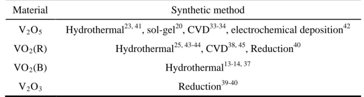
Table 1.1 Synthetic routes for different vanadium oxides with 1D nanostructure.
... 13
Table 1.2 FE parameters of 1D nanostructures in the previous study ... 23
Table 2.1 Parameter of reduction reaction and refined cell parameter of
as-obtained reduced product ... 27
Table 2.2 Parameter and final product of two reduction system ... 29
Table 2.3 FE properties as-prepared product NWs ... 41
Table 3.1 Reaction conditions and morphology properties of Na
0.24V
2O
5NWs
identified with SEM ... 54
Table 3.2 Comparison of FE properties between as-prepared product and V
2O
5NWs ... 59
List of Figures
Figure 1.1 Projection of the V
2O
5crystal structure along (a) [100] and (b) [010]
axis. ... 5
Figure 1.2 Coordination of vanadium with oxygen in vanadium pentoxide. ... 5
Figure 1.3 Projection of the VO
2(R) structure along (a) [100] and (b) [010] axis.
... 7
Figure 1.4 Conductivity as a function of reciprocal temperature for the lower
oxides of titanium and vanadium. Measurements were made along the [100]
direction in VO, and along the c axis in V
2O
3and VO
2(R).
31... 8
Figure 1.5 (a) Projection of the VO
2(B) structure along [010]. There are
packing of edge sharing octahedra that are only linked by corners in (a,b) planes.
Octahedra at y=0 and y=1/2 are, represented yellow and blue, respectively. (b)
One (010) plane for the idealized VO
2(B) structure. Note that, with respect to
the perfect oxygen bcc lattice, there are oxygen vacancies. ... 10
Figure 1.6 One (001) plane for the V
2O
3structure. It shows a hcp arrays of O
atoms (yellow) with vanadium atoms (red) occupied at 2/3 octahedral sites. .... 11
Figure 1.7 The projection of
β
-Na
xV
2O
5crystal structure along [010]. ... 15
Figure 1.8 Schematic illustration of the hot-wall, low pressure CVD reactor
proposed by Shivashankar.
61... 17
Figure 1.9 Schematic illustration of experiments to deposit V
2O
5NWs on the
surface of a substrate.
62... 19
Figure 1.10 Energy diagram of metal-vacuum level (a) without electric field, (b)
under high electric field. ... 20
Figure 2.1 the XRD profiles of (a) V
2O
5, (b) VO
2(R), (c) VO
2(B) and (d) V
2O
3.
Figure 2.2 Top view SEM image and corresponding side view image (inset) of
(a) V
2O
5, (b) VO
2(R), (c) VO
2(B), (d) V
2O
3NWs thin-film. ... 34
Figure 2.3 TEM (left), SAED (right top), and HRTEM (right bottom) images of
as-obtained (a) V
2O
5, (b) VO
2(R), (c) VO
2(B), (d) V
2O
3NWs, respectively. .. 34
Figure 2.4 High magnitude resolution of side view image of as-prepared (a)
V
2O
5, (b) VO
2(R), (c) VO
2(B), (d) V
2O
3NWs ... 35
Figure 2.5 XPS spectrum for V-2p region of as-prepared (a) V
2O
5, (b) VO
2(R),
(c) VO
2(B), (d) V
2O
3NWs thin film, respectively. ... 37
Figure 2.6 Schematic illustration of transformative evolution. It shows single
atom layers of (a) V
2O
5, (b) VO
2(R), (c) VO
2(B), (d) V
2O
3along their
corresponding growth plane. ... 39
Figure 2.7. The plot of Field emission current density verse applied electric
field and its corresponding Fowler-Nordheim plots (inset) of as-prepared (a)
V
2O
5, (b) VO
2(R), (c) VO
2(B), (d) V
2O
3NWs thin-film, respectively. ... 41
Figure 3.1 The calculated XRD pattern and the XRD profiles of typical product
synthesized at the temperature of (a) 300°C, (b) 350°C and (c) 400°C. ... 48
Figure 3.2 (a) Top view SEM image of Na
0.24V
2O
5hin-film and side view in
inset (b) TEM (left), SAED (right top), and HRTEM (right bottom) images of
as-obtained Na
0.24V
2O
5NWs. ... 49
Figure 3.3 (a) Overall XPS spectrum and (b) high-magnification XPS spectrum
for V-2p region of the NWs of Na
0.24V
2O
5... 50
Figure 3.4 The side view images of as prepared Na
0.24V
2O
5NWs thin-films
synthesized at (a) 300°C, (b) 350°C and (c) 400°C, respectively. ... 52
Figure 3.6 The side view images of as prepared Na
0.24V
2O
5NWs thin-films
synthesized by using Na-solution of concentration (a) 0.125M, (b) 0.025M and
(c) 0.05M, respectively. ... 53
Figure 3.7 The XRD pattern of typical intermediate product synthesized at
during period of (a) 15 minutes, (b) 30 minutes, (c) 45 minutes. ... 55
Figure 3.8 Schematic illustration of reaction mechanism to deposit
β-Na
xV
2O
5NWs on the surface of a substrate ... 56
Figure 3.9. UV–visible absorption spectrum and the plot of (
α
h
υ
)
2versus
incident photon energy h
υ
(inset) for the Na
0.24V
2O
5thin-film as prepared ... 57
Figure 3.10 Field emission current density as a function of an applied electric
field of as-prepared Na
0.24V
2O
5NWs thin-film. Inset shows its corresponding
Fowler-Nordheim plots. ... 59
Chapter 1.
Introduction
1.1 Brief review of 1D Nanomaterials
In the past decades, the word "nanotechnology" has been widely mentioned, which means any technology based on nano-scaled materials for any application in the real world. Nanotechnology includes the production and application of physical, chemical, electronic, and biological systems at scales ranging from 1 to 100 nanometers, and the length of 1 nm equals a row of 10 hydrogen atoms. When scale size of material was shrunk to nano-level, the properties of materials behave differently compared to previously bulk ones. For example, gold shows the various color (orange, red, purple, blue) when particle size was changed from 1 to 500 nm.1 The energy band gap of Si rose from 1.12 eV to 2.60 eV when the size scale of Si was lowered down to 3nm3.2
Investigation of one-dimension (1D) nanomaterials was one portion of nanoscale materials. It is generally accepted that 1D nanostructures are more prone to charge transport than the bulk crystalline structures. In addition, 1D nanomaterials can demonstrate the characteristics of field emission owing to quantum tunneling effect.3-4 They are also expected to as potential candidates for both interconnect5 and functional units in fabricating sensor,6 electronic, optoelectronic7, thermoelectric8-9 and electrochemical10-12 devices with nanoscale
nanotube10, 13-15 forms were developed in recent years, which have raised much attention for their peculiar physical properties and their potential applications.7, 16-19 Among these metal oxide materials, 1D nanostructure for vanadium family oxides, including binary and ternary vanadium oxide, shows diverse physical and chemical properties in electronic, thermochromic, magnetic, and optoelectronic properties for their variable oxidation states, which have been widely applied on chemical sensors20-23, ultrafast optical switchers, electrochromic24, thermochromic25 devices. Furthermore, the unique structural features also allow the application on rechargeable lithium battery for serving as electrodes.11
In this thesis, we are going to reveal the growth of kinds of vanadium family oxides with nanowires morphology, including V2O5, VO2(R), VO2(B), V2O3, and a ternary phase
β-NaxV2O5, via a series of procedure containing thermal evaporation, pre-treatment of
substrate, and post- reduction treatment. Crystalline, morphology, growth mechanism, and field emission properties of these nanowires and thin-film are deliberated in detail.
1.2 Family of Vanadium Oxide
Within the family of metal oxide, researches of vanadium oxides have been particularly focused in recent years for their diverse electronic, electrochromic, thermochromic, magnetic, and optoelectronic properties. Vanadium adopts different valence states, which can afford several oxidized structures. Besides, single-valence compounds such as VO, V2O3, VO2 and
V2O5, a number of mixed-valence oxides, e.g., V6O13 or V10O24, have been reported.26-27
Specifically, in this manuscript, we are interested in V2O5, VO2 and V2O3, each of which has
raised more attraction owing to their natural properties. The brief reviews of these vanadium oxides will be introduced clearly in the following section.
1.2.1 Structure, Properties and Application
1.2.1.1 V2O5
The structure of V2O5 crystallizes in orthorhombic unit cell with lattice parameter of a =
11.51 Å, b = 4.36 Å, c =3.56 Å; and the space group is Pmn21. V2O5 adopts a layer
framework with large V–O separation along the crystallographic b direction. (see Figure 1.1a) In V2O5, V atom is coordinated with five oxygen atoms and forms a VO5 square pyramid.
Along c-axis, VO5 square pyramids are linked by sharing edge and results in a zigzag chain
Figure 1.2. The vanadium atom has coordinated with five oxygen atoms (V–O bond lengths vary from 1.585 Å to 2.021 Å): one with O1 atoms, one with O2 atoms and three with O3
atoms. The distance between V atom and O1*atom located at neighboring layer are too far
away, leading to weak V-O1* bond and the layer structure.28 In the family of vanadium
compound, V2O5 is the most stable one with the highest oxidation state and exhibits peculate
layer structure, which are expected to be potential material for applications in chemical sensor, catalyst, electrochemical cell, and photoelectric devices. For example, Zarbin and co-workers fabricate V2O5 nanoparticles to be a cathodic material for Li+-based batteries.29 The study
showed that the two-dimensional layer structure of V2O5, which favors intercalation of guest
species, with high charge density and electrochemical stability makes this compound an attractive cathodic material for lithium rechargeable cells. Liu et al. had prepared the single crystal V2O5 nanofibers to be an ethanol sensor material.21 The V2O5 nanobelts are n-type
semiconductor and the charge transport proceeds via electron hoping between V4+(impurity) and V5+ centers. When the reducing gases like ethanol are attached to the oxygen adsorbates (O- or O2-) covering on the surface of V2O5 nanobelts by hydrogen bond, the charge carriers
(V4+) will increase owing to charge transfer from oxygen adsorbates to belts. The study showed that V2O5 have excellent potential for sensor application.
Figure 1.1 Projection of the V2O5 crystal structure along (a) [100] and (b) [010] axis.
1.2.1.2 VO2(R)
Vanadium dioxide (VO2) is a traditional binary compounds with several allotropic phase,
including VO2(R), VO2(B), VO2(A).30 The VO2(R) with rutile monoclinic structure (space
group : P21/c (14)) is the most stable phase in thermodynamic concern. The projection of the
VO2(R) structure along [ 1 0 0 ] has been shown in Figure 1.3a, which gives a distorted rutile
structure. In VO2(R), vanadium atoms are coordinated with five oxygen atoms and form an
octahedral geometry, with their axial axes aligned alternatively along [ 0 1 1 ] and [ 0 -1 1 ]. The octahedron is not regular which contains one shorter V-O bond length of 1.7 Å and leads to distorted rutile structure with lower symmetry. The adjacent octahedra share edges along the a-axis to form chain structure. (see Figure 1.3b) The 21 symmetry can be found on
bc-plane and the chain structures are connected by sharing their corners to build a 3D network.
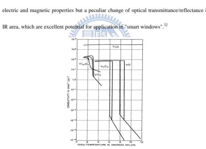
VO2(R) possesses unique semiconductor-to-metal phase transition (SMT) at around
340K. Below the phase transition temperature, VO2(R) shows semiconductor behavior with a
monoclinic crystal (distorted rutile structure), and exhibits the optical property with IR transparent. Above the transition temperature, VO2(R) converts to tetragonal crystal (regular
rutile structure) and shows an abrupt improvement in resistivity beyond (see Figure 1.4).31 It becomes a metal-like material, and the optical property changes to IR reflection. Accompanied with the phase transition, VO2(R) shows not only a reversible abrupt change of
electric and magnetic properties but a peculiar change of optical transmittance/reflectance in IR area, which are excellent potential for application in "smart windows".32
Figure 1.4 Conductivity as a function of reciprocal temperature for the lower oxides of
titanium and vanadium. Measurements were made along the [100] direction in VO, and along the c axis in V2O3 and VO2(R).31
1.2.1.3 VO2(B)
The other phase of VO2, VO2(B) have a little in common with the rutile phase. VO2(B)
possesses larger monoclinic unit cell than that of VO2(R) with lattice parameter of a = 12.03
Å, b = 3.69 Å, c = 6.42 Å, and β = 106.6° and the space group is C2/m(12). The VO2(B)
structure can be considered as regular-stacked identical layers of atoms along b axes. Figure 1.5 shows the arrangement of polyhedron in the ( 0 1 0 ) plane of VO2(B) and the second
layer is shifted with respect to the first one by 1/2, 1/2, 0. In this structure, V-O also forms a six-coordinated environment with slight distortion. The fourfold axes of the octahedra are more or less aligned along a single crystallographic direction, namely, [ 0 1 0 ]. Figure 1.5b shows a single layer of ( 0 1 0 ) plane for the ideal VO2(B) structure. The structure is based on
an oxygen hcp array with ordered oxygen vacancies, drawn here with hollow red circle. Vanadium atoms further occupy in residual octahedral sites.30 Along b-axis, the layer structure stacks through edge-sharing to form a 3D framework.
Figure 1.5 (a) Projection of the VO2(B) structure along [010]. There are packing of edge
sharing octahedra that are only linked by corners in (a,b) planes. Octahedra at y=0 and y=1/2 are, represented yellow and blue, respectively. (b) One (010) plane for the idealized VO2(B)
1.2.1.4 V2O3
V2O3 crystallizes in Al2O3 (corundum) structure with a hexagonal unit cell (space group:
R-3c (167)) and the lattice parameters are a = 4.95 Å, b = 4.95 Å, c = 14.00 Å. Figure 1.6
shows the projection of [0 0 1] direction for the V2O3 structure, the structure is based on an
oxygen hcp array with vanadium locating at 2/3 octahedral sites.
V2O3 also undergoes the semiconductor-to-metal phase transition (SMT) with a lower
temperature (~-120°C).31
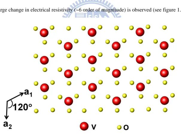
During the phase transition process, an insulating, antiferromagnetic phase with monoclinic crystal converts to metal-like phase with corundum structure and a large change in electrical resistivity (~6 order of magnitude) is observed (see figure 1.4).
1.2.2 Literature Review of Vanadium Oxide
In the past decades, the fabrication of vanadium oxides with 1D nanostructures has been researched intensively. A variety of methods, such as CVD33-34, hydrothermal route23, sol-gel20, have been developed to prepare vanadium oxides with 1D nanostructure. Table 1.1 summarizes the synthetic method for different vanadium oxides with 1D nanostructure in previous report.
In fact, V2O5 tends to form 1D and 2D nanomaterials owing to peculiar layer structure.
Recently, lots of groups have proposed a variety of methods such as hydrothermal, sol-gel, CVD ,and electrochemical deposition to control the formation of V2O5 1D nanomaterials. For
example, Zhou et al. grew V2O5 nanobelts from the reaction of ammonia metavanadate with
nitric acid under thermal treatment.35 Raible and coworkers had used sol-gel method to synthesis V2O5 nanofibers, whose lengths could be controlled by adjusting the reaction period. 20
Bando fabricated V2O5 nanowires with centimeter length via a hydrothermal reaction in an
aqueous solution of V2O5 and H2O2.36
However, less synthetic routes are suitable to fabricate the 1D nanomaterial of reduced vanadium oxides (VO2(R), VO2(B), V2O3). A common preparative procedure for 1D
nanostructure vanadium dioxides of VO2(R) and VO2(B) involves the hydrothermal treatment
of vanadium precursor with reducing agents. For example, Sediri et al. have reported the use of aniline as both reducing agent and structural templating agent for the preparation of VO2(B)
nanoneedles from bulk V2O5 powder.37 Ji and co-workers successfully fabricated single
crystal VO2(R) nanorods from the reaction of the bulk V2O5 powder under hydrothermal
treatments in the presence of oxalic acid as reducing agent and H2SO4(aq) as acidifying agent,
respectively.25 VO2(R) with 1D nanostructures has also been synthesized via PECVD first
reported by Guiton et al..38 They hadsuccessfully deposited VO2(R) nanowires on the Si3N4
substrates from VO2(B) powder as a vanadium source under thermal evaporation
(900°C-1000°C) with the assistance of the carrier gas flow of Argon gas. V2O3 with 1D
nanostructure have only been synthesized through reduction reaction from V2O5 or VO2 to
V2O3. For example, Santulli et al. first prepared VO2 nanorods by hydrothermal treatment,
and further reduced it to V2O3 in the presence of reducing gas.39 Corr and co-workers
reported a systematic reduction of V2O5 nanoscrolls to VO2(R) and V2O3 by adjusting
reduction temperature and duration time.40
Table 1.1 Synthetic routes for different vanadium oxides with 1D nanostructure.
Material Synthetic method
V2O5 Hydrothermal23, 41, sol-gel20, CVD33-34, electrochemical deposition42
VO2(R) Hydrothermal25, 43-44, CVD38, 45, Reduction40
VO2(B) Hydrothermal13-14, 37
1.3 Ternary Phase of Bronze Vanadium Oxide
β
-Na
xV
2O
5Recently, the research in low dimensional metal oxide nanomaterial has been focused on ternary phase such as NaV6O15, Zn2SnO4, ZnMgO, and etc. 1D nanostructure for bronze
vanadium oxides, such as β-NaxV2O5, AgV6O15, K2V8O21, CaV6O16, are well known to
exhibit a wide range of practical applications.22, 46-50 Owing to their unique structural feature combined with chemical and physical properties, they are good candidates for serving as a electrodes for rechargeable lithium battery51, supercapacitors52, and other else. In this study, the interesting 1D nanomaterial of β-NaxV2O5 is the target product, and it will be introduced
clearly in the following section.
1.3.1 Structure and Properties
β-NaxV2O5 is a member of the vanadium bronzes MxV2O5 ( M=alkali, alkaline, earth
and metal) family. MxV2O5 are mixed-valence compounds, whose structure, magnetic, and
electronic properties are demonstrated by the M cationic species and the concentration x. The β phase is located around stoichiometric concentration of x = 0.23-0.41. The β-NaxV2O5
possesses a monoclinic unit cell with space group of C2/m, and Figure 1.7 shows the unit cell of β-Na0.33V2O5 containing six NaV6O15 formula unit. In the structure of β-Na0.33V2O5, the
V-O framework comprises of the three distinct types of double chains directed along the b axis. The V1-site has a six-coordinated octahedral geometry and forms a zigzag chain by
edge-sharing. The V2 site with a similar octahedral coordination form a two-leg ladder chain of corner-sharing VO6 octahedra, and the V3 site, having a fivefold square pyramidal
coordination constructs a zigzag chain of edge-sharing VO5 pyramids. The Na+ ions are
located in the tunnels formed by above V-O framework. In the case of concentration x = 0.33, the Na+ ions occupy only one of two nearest-neighboring site A on ac plane. The electrons of the Na+ ions are transferred into the d shells of V ions, resulting in the mixed valence states V4+ (d1) and V5+ (d0).53 Precious study had demonstrated that in the high temperature, T > 136K, the donated electrons are situated at the V1 site, with one half of two V1 site being V4+.54 These features make β-NaxV2O5 possesses novel physical, magnetic and
superconductive properties at a critical condition.55-57
1.3.2 Literature Review of β-NaxV2O5
Recently, β-NaxV2O5 has been synthesized with 1D Nanostructure through CVD and
hydrothermal route. The hydrothermal method involves the reaction between V2O5 and
sodium precursor in the presence of reducing agents. For example, Yu et al. first reported a general route for the synthesis of NaV6O15 single-crystal nanowires based on hydrothermal
treatment between V2O5 and NaHSO4⋅H2O.58 They also successfully synthesized NaV6O15
nanoneedles by changing the sodium precursor, NaHSO4⋅H2O(aq) to PSMA-Na(aq).59 Zhou
and co-workers successfully fabricated single crystal NaV6O15 nanorods from the reaction of
bulk V2O5 powderunder hydrothermal treatment in the presence of NaCl as sodium precursor
and H2O2 (aq) as reducing agent, respectively.51
Another preparative method based on CVD was proposed by Shivashankar60, and the installment is shown in Figure 1.8. They successfully deposited single crystal NaxV2O5 NWs
on the surface of sodium silicate glass with the assistance of Ar/O2 flow as carrier gas. In this
study, the source of Na+ ions were from the glass substrate that diffused into the vanadium oxide precursor and further reacted to form β-NaxV2O5 nanowires.
1.3.3 Application
β-NaxV2O5 possesses a more rigid 3D network that is different from the V2O5 with
in the mixed-valence states V5+(d0) and V4+(d1). Recently, this particular feature is expected to improve the property of ions transport, charge storage and electronic transport for applications like supercapacitors and cathode material in lithium battery. For example, Zhou and co-workers used single crystalline NaV6O15 nanorods to serve as a cathode material for
rechargeable lithium battery and obtained a high electrochemical performance upon lithium insertion and extraction.51 Lee et al. had successfully fabricated β-Na0.33V2O5 nanobelts via
hydrothermal route and used that as an electrode for supercapacitor.52 The three dimensional framework crystal structure of the β-Na0.33V2O5 nanobelts network electrode shows a high
specific capacitance of 320 F⋅g-1
and only 34% degradation in specific capacitance being observed in galvanostatic cycling testing after 4000 cycles. These results suggested that the β-Na0.33V2O5 nanobelt network structure is a potential energy storage material.
Figure 1.8 Schematic illustration of the hot-wall, low pressure CVD reactor proposed by
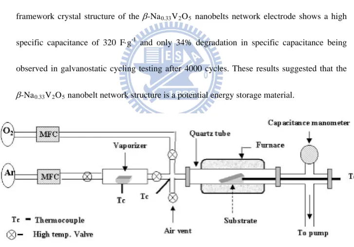
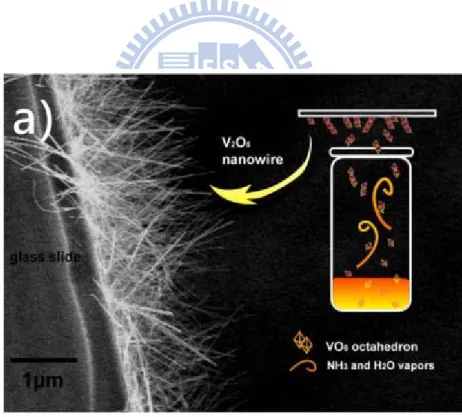
1.4 Thermal Evaporation-Like Synthesis for Vanadium Oxide NWs
Recently, we applied a facile route to control the growth of nearly aligned MoO3 and
V2O5 nanowires (NWs) on varies substrates based on thermal evaporation.62-63 In the case of
V2O5, the V2O5 nanowires were deposited on the surface of glass substrate as following: First,
a mixture of V2O5 powder (0.1g, 0.55mmole) and NH2OH⋅HCl(aq)(3M, 2mL) was placed in a
glass vial stirring at 50oC. After the color of mixture turned from orange to blue, a glass slide rinsed by ethanol and deionized-water was covered on the top of the glass vial. Thereafter, this installation was transferred to a programming furnace. The temperature was raised to 400°C over duration of 1 hour, and the V2O5 nanowires were grown on the surface of glass
slide; a schematic illustration appears in Figure 1.9.
Initially, the dispersed bulk V2O5 powder was reduced by NH2OH⋅HCl(aq) to form a
pre-mixture with blue color indicative of the formation of polyvanadate species (VOx).
During the thermal treatment, the polyvanadate species were transport to the surface of glass with the assistance of H2O(g) and NH3(g) (vaporized from decomposed NH2OH⋅HCl). During
calcination with elevated temperature, the polyvanadate species stacked and crystallized, leading to growth of NW-formed V2O5. The study demonstrated that the presence of
NH2OH⋅HCl in the growth process was found to be essential, which was not only provided
the H2O and NH3 vapor source but also reduced V2O5 to polyvanadate species dissolved in
Comparing with other synthetic routes (hydrothermal, sol-gel, etc.) which suffer from long reaction time and complicated cleanup procedures, and this thermal evaporation method exhibits the advantages of simple, economical, mild and time-saving treatment for preparing V2O5 nanowires thin film on the substrate directly. Moreover, this method is anticipated to be
applied to fabricate various metal-oxide nanocrystals on oxide substrates with special crystal morphologies on choosing a suitable precursor. Owing to these features, this thermal evaporation method still possesses much potential development and is worth to continually study.
Figure 1.9 Schematic illustration of experiments to deposit V2O5 NWs on the surface of a
1.5 Theory of Electron Field Emission
1D nanostructures, such as nanobelts, nanorods, nanotubes, and nanowires, have raised much attention in the field emission application owing to their unique electrical properties, chemical stability, and high aspect ratios in appearance of these materials. Electron field emission (EFE) is a quantum tunneling phenomenon of electron from the surface of a material subjects to a strong electron field. The energy diagram of a metal-vacuum system without external electric field is shown in Figure 1.10a. When a sufficiently high field was applied on a metal or semiconductor, electrons will tunnel through the surface potential barrier of the sample surface into vacuum level. As shown in Figure 1.10b, the vacuum level is bent and reduced at extremely high electric field. Energy barrier between the surface of metal and the vacuum become so narrow that the electron can tunnel through it easily, even at very low temperature.
Figure 1.10 Energy diagram of metal-vacuum level (a) without electric field, (b) under high
Fowler and Nordheim obtained the accurate description of field emission, based on tunneling of electrons through the surface potential barrier, in 1928.64 Considering the emission of electrons from a object, the emission current defined by multiplying the number of electrons N(W,T) is determined to multiply the flux of electron incident on the surface potential barrier and the tunneling probability of electrons to overcome the potential barrier as shown below.
0
( , ) ( , ) ( )
J E T =e
∫
∞N W T D W dW (1.1)When E, T represent the applied electric field and the temperature, N(W,T) and D(W) are the function of E, and T. By integrating equation (1.1), it will change into
1/ 2 3 2 3/ 2 0 0 2 2 2 0 0 4 2 ( , ) exp ( ) 16 ( ) sin( ) 3 B B c k T e E m J E T v y h t y c k T e h E π φ π φ π = − (1.2) while the time factor is
1/ 2 4 0 3.79 10 E y = × − φ (1.3) The velocity is
( )
0 V y (1.4)Set T approximate to zero to discuss the field emission, equation (1.2) could be shown as
3/ 2 2 ( ) exp B J F AF F φ − = (1.5) while 3 2 16 ( ) e A t y π φ ≡ , and
( )
1/ 2 0 2 4 2 3 m B v y e ≡ This is known as Fowler-Nordheim equation. Under the field emission condition, y is between 0-1, and the function of v(y) and t2(y) could be approximated to:
2 2
( ) 1.1 , ( ) 0.95
t y = v y = − y
By substituting the approximation above, J = I/α, and F = βV into equation (1.5), the expression becomes 2 b I aV exp V − = (1.6) where 2 7 1/ 2 (1.44 10 ) exp 1.1 A B a α β φ φ − × = and 3/ 2 0.95B b φ β = A = 1.54×10⁻⁶, B = 6.87×10⁻⁷ .
A denotes the effective emission area and β is the field enhancement factor. There are three factors, α, β, and φ, in equation (1.6) could influence the magnitude of the field emission current density. equation (1.6) can be further expressed as
2 1 ln I lna b V V = − (1.7) As a consequence, for a field emission data, by plotting of log(I/V2) versus 1/V, a straight line with negative slope could be obtained, and was designated as F-N plot. Through this plot, one can judge the field emission properties of a sample. When the work function of the sample is known, the field enhancement factor could be calculated from the slope of F-N plot.
Table 1.2 FE parameters of 1D nanostructures in the previous study
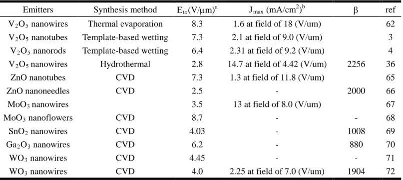
Emitters Synthesis method Eto(V/µm)a Jmax (mA/cm2)b β ref
V2O5 nanowires Thermal evaporation 8.3 1.6 at field of 18 (V/um) 62
V2O5 nanotubes Template-based wetting 7.3 2.1 at field of 9.0 (V/um) 3
V2O5 nanorods Template-based wetting 6.4 2.31 at field of 9.2 (V/um) 4
V2O5 nanowires Hydrothermal 2.8 14.7 at field of 4.42 (V/um) 2256 36
ZnO nanotubes CVD 7.3 1.3 at field of 11.8 (V/um) 65 ZnO nanoneedles CVD 2.5 - 2000 66 MoO3 nanowires 3.5 13 at field of 8.0 (V/um) 67
MoO3 nanoflowers CVD 8.7 - - 68
SnO2 nanowires CVD 4.03 - 1008 69
Ga2O3 nanowires CVD 6.2 - 880 70
WO3 nanowires CVD 4.45 - - 71
WO3 nanowires CVD 4.0 2.25 at field of 7.0 (V/um) 1904 72
1.6 Aim of This Thesis
Vanadium oxides and their derivatives exhibit outstanding chemical and physical properties, which are used in many fields. A facile and economical way to grow vanadium oxides NWs represents a significant improvement for application in future nanodevices. The conventional synthetic routes suffer from time-consuming, complicated procedure, and uneconomic. Previously, our group reported a facile route to control the growth of nearly aligned V2O5 and MoO3 nanowires on varies substrates based on thermal evaporation. It is
anticipated that the synthetic procedure is suitable for preparing other 1D metal oxides.
In this thesis, we extend this deposition process to obtain binary and ternary phase of vanadium oxides with 1D nanostructure. We tried to combine the original thermal evaporation procedure with post-reduction treatment to obtain reduced vanadium oxide. In the first part, V2O5 NWs thin-films were first deposited on the surfaces of substrates via a thermal
evaporation route. The reduced vanadium oxide phase of VO2 and V2O3 NWs were obtained
by adjusting the experimental parameters of reduction. In the second part, the target product we planned to prepare is β-NaxV2O5, and a well–controlled Na+ ion source is necessary.
Based on this concept, a modified thermal evaporation with an surface pre-treatment of substrate was developed. The sodium silicate is used as the source of the sodium ion, which was first coated on the substrates and the amount of precursor was carefully controlled on a Na+-free substrate. The polyvanadate species are delivered to the surface of substrate during
evaporation process, which were further react with Na+ ion to form a ternary compound of β-NaxV2O5.
Several analytical techniques were used to confirm the nature of as-prepared typical product, and the crystalline, morphology, reaction condition, and growth mechanism of these nanowires and thin-film would be discussed in detail. Finally, field emission properties of these NWs sample are demonstrated and studied in this work.
Chapter 2.
Controlled Reduction of Nearly-Aligned Nanowires of V
2O
5to
VO
2(R), VO
2(B) and V
2O
32.1 Introduction
In the previous section, we mentioned a facile route to control the growth of nearly aligned MoO3 and V2O5 NWs on varies substrates. The as-synthesized V2O5 NWs on
substrate were further used as a precursor to prepare reduced vanadium oxide nanowires with controlled reduction conductions. In this section, we had set a systematic reduction condition and successfully obtained several reducing vanadium oxide phase of VO2(R), VO2(B), and
V2O3 by adjusting reaction period or the composition reducing gas flow. The structural
information of reducing vanadium oxide nanowires was investigated with various analytic
techniques such as SEM, TEM, SAED, XRD, and XPS. In addition, field emission
measurements were carried out and the results show small actuation voltages and a large
current density of reducing vanadium oxides NWs arrays, which properties are prospectively
2.2 Experimental
2.2.1 Synthesis
2.2.1.1 The V2O5 nanowires film
V2O5 nanowires were grown on a substrate with a thermal evaporation method
developed in previous study. The details of the deposition procedures are described elsewhere.
2.2.1.2 The Reduction of the Nanowires Thin Film
Before reduction reaction, V2O5 NWs were examined with P-XRD to check the purity.
Initially, pure V2O5 nanowires thin film was placed in an alumina crucible, which was
subsequently placed in a tube furnace. The reduction reaction proceeded with constant heating rate 200oC hr-1 and kept at the 450°C. The vanadium oxide nanowires with different oxidation states were obtained by adjusting the composition of the reducing gas and the reaction period, and the parameters were summarized in Table 2.1.
Table 2.1 Parameter of reduction reaction and refined cell parameter of as-obtained reduced product
Product
Parameter of reduction Refined cell parameter composition Temp. duration lattice
Space
group a(Å) b(Å) c(Å) β(°) VO2(R) 10%H2/90%Ar 450°C 12 hours monoclinic P21/c 5.74 4.53 5.38 122.65
VO2(B) 100% H2 450°C 2 hours monoclinic C2/m 12.03 3.69 6.39 106.88
V2O3 100% H2 450°C 4 hours hexagonal R-3c 4.94 4.94 13.99 -
2.2.2 Characterization
The crystalline were measured by powder X-ray diffraction (XRD, Bruker AXS D8 Advance, Leipzig Germany) with Cu-Kα radiation operating at 40kV, 40 mA. The micrographs of scanning electron microscope (SEM, Hitachi, S-4700I, operated at 15kV) and transmission electron microscope (TEM, JEOL, JEM-3000F, operated at 200kV) were used to determine the morphology and the size of nanowires. The samples for TEM experimental were prepared as-following: first, the NWs were separated from glass by ultrasonic dispersion of the thin film in ethanol for 5 minutes. Then, the dispersion solution was dropped onto a copper grid (carbon film-coated 100 mesh), and dried in air atmosphere leaving spread NWs on the carbon film. X-Ray photoelectron spectroscopic analysis was made with a XPS spectrometer (PHI Quantera SXM); the binding energy was calibrated by use of the C-1s line at 284.4eV. For field emission measurement, the vanadium oxide thin films were placed into a vacuum chamber with a pressure less than 3×10⁻⁷ Pa at room temperature. The distance between the electrode and sample was fixed at 100µm and the high-voltage sourcemeter (Keithly 2410) was used to measure the current-to-voltage characteristics.
2.3 Results and Discussion
2.3.1 Synthesis and Reduction Condition
To prepare vanadium oxides NWs thin film with various oxidation states, the as-prepared V2O5 NWs were heated in a tube furnace under H2/Ar pre-mixed gas with specific
composition and flow rate of 0.4 SLPM (Standard Liter Per Minute). The initial attempt to reduce V2O5 thin film was carried out under ambient concentration of H2/Ar pre-mixed gas.
It was found out that the VO2(R) and VO2(B) can be synthesized with low and high
concentration of H2, separately. On the basis of this finding, we set two reduction systems to
control the product of reduced vanadium oxide. All parameters and results of the reduction condition are referred in Table 2.2, and the pure phase of reduced vanadium oxides were obtained according to the condition presented in Table 2.1.
Table 2.2 Parameter and final product of two reduction system
System temperature composition duration product 1 Mild Reduction System 450°C 10%H2 6hr V2O5 2 450°C 10%H2 9hr V2O5+VO2(R) 3 450°C 10%H2 12hr VO2(R) 4 Rapid Reduction System 450°C 100%H2 2hr VO2(B) 5 450°C 100%H2 4hr V2O3 5 450°C 100%H2 6hr V2O3
2.3.2 Structural and Purity Characterization
The crystallinity and purity of as-prepared NWs were confirmed by using powder XRD, as shown in Figure 2.1. The XRD profile of for V2O5 NWs can be indexed as orthorhombic
unit cell (JCPDS number: 72-0589, space group: Pmn21; a = 11.45 (2) Å, b = 4.430 (6) Å, c =
3.542 (3) Å). Figure 2.1b shows the XRD pattern of reducing product obtained at mild reduction condition (condition 1), which corresponds to monoclinic rutile VO2 (JCPDS
number, space group :43-1051) On the other hand, rapid reducing conditions (condition 2 and 3) preferred to form VO2-B (Figure 2.1c, JCPDS number: 65-7960) and V2O3 phases (Figure
2.1d, JCPDS number: 84-0316). Refined lattice parameter of all reducing product were referred in Table 2.1. The XRD profile of VO2(R) and VO2(B) show low signal-to-noise
ratios for all diffraction peaks, indicative of low yield and the formation of amorphous phase. According to these results, we assume that the reduction reaction can be regarded as continuous process, and the vanadium oxide will be reduced continually by hydrogen. The transformation of V4+ into V3+ occurs immediately after the conversion of V5+ to V4+. V4+ can be defined as the transition state during the reduction reaction and we limit the duration time to cease the reaction and preserve the vanadium oxide with V4+ state. Furthermore, the amorphous VOx (oxidation states of V and III) are also preserved at the same time and PXRD
profiles reveal a low signal-to-noise ratio. The lowest oxidation state of vanadium ion is +3 in V2O3. When the duration time of reduction was increased, the amorphous VOx species would
be completely converted to V2O3 and crystallize, which results in a PXRD pattern with good
signal-to-noise ratio.
2.3.3 The Morphology and Structure of As-Obtained Typical Product
The representative morphology and structure of as-prepared NWs were investigated by FE SEM and TEM, as shown in Figure 2.2 and Figure 2.3, respectively. Figure 2.2a shows the SEM image of V2O5 NWs,and the microstructures of that are long uniform nanowires. Large
portion of V2O5 NWs possesses length of up to tens of micrometer as calculated from SEM
image. Other SEM image (see Figure 2.4) also confirm the NWs structure of V2O5 with width
of 70~150nm. The side view image (inset of Figure 2.2a) clearly reveals that V2O5 NWs are
nearly vertical-aligned to the surface of the glass. Figure 2.2b-2.2d show the SEM images of the reduced product, and the insets are their corresponding side view image. The results suggest that the large portions of NWs microstructure are maintained with nearly vertical-aligned structure to the surface. It is demonstrated that the morphology is not destroyed during the reduction reaction.
Figure 2.3a shows the TEM image of a single V2O5 NW and insets show its
corresponding selected area electronic diffraction (SAED) pattern (top) and high resolution-TEM (HR-TEM) image (bottom). The SAED pattern and HRTEM image of a single wire recorded from [0 1 0] zone axis, and SAED pattern reveals sharp and clean diffraction spots, indicative of single crystalline property. HRTEM image indicates lattice fringe of 5.72Å and 3.39Å, corresponding to (2 0 0) and (1 0 -1) crystal planes for orthorhombic V2O5, respectively. The growth direction is along the c-axis, which is deduced
from the angle of 90° between the c-axis and the a axis, consistent with the previous studies. Figure 2.3b-2.3d show the TEM images of single NW of reduced products and insets show their corresponding SAED pattern (top) and HR-TEM image (bottom). The SAED pattern and HR-TEM of VO2(R), VO2(B), and V2O3 single wire were recorded from zone axis of [2 -1 1],
[0 0 1], and [2 -2 1], respectively. All SAED pattern of reduced product also exhibits sharp and clean diffraction spots owing to single crystalline property. The HR-TEM taken of a portion of VO2-R NWs reveals parallel lattice fringes with inter-layer distance ~3.31 Å and
3.19 Å, which corresponding to plane (1 1 -1) and (0 1 1). Combined with the TEM image, the growth direction of VO2(R) NW is closed to the vector which is perpendicular to the plane
(1 1 -1). The HR-TEM of VO2(B) NWs shows the d-spacing of 3.5 Å and 5.7 Å, consistent
with that of the (1 -1 0) and (2 0 0), respective. The growth direction of VO2(B) NW is along
the b-axis, which is deduced from the angle of 90° between the b-axis and the a axis. As shown in Figure 2.3d, the marked interplanar d-spacing of 2.5 Å and 5.0 Å corresponds to the (0 1 -2) and (1 -1 4) lattice plane of hexagonal V2O3. The results of SAED and HR-TEM
demonstrate that the V2O3 NWs are single crystalline in structure along growth direction of
the normal vector of plane (1 1 0), which can be deduced by using the angle of 90° between two normal vector of plane (1 1 0) and (1 -1 4). The crystal growth directions of all reduced products are suggested by SAED and HR-TEM analyses, and that is influenced by the
Figure 2.2 Top view SEM image and corresponding side view image (inset) of (a) V2O5, (b)
VO2(R), (c) VO2(B), (d) V2O3 NWs thin-film.
Figure 2.3 TEM (left), SAED (right top), and HRTEM (right bottom) images of as-obtained
Figure 2.4 High magnitude resolution of side view image of as-prepared (a) V2O5, (b)
2.3.4 X-Ray Photoelectron Spectroscopic Analyses.
XPS analyses have been further achieved to investigate the information of the oxidation state of vanadium ions in as-prepared product. As shown in Figure 2.5, the high resolution XPS spectra for V 2p region shows the binding energy of V 2p1/2 and V 2p3/2. The peak in V
2p3/2 spectrum of VO2R and VO2B (Figure 2.5b and 2.5c) are broad ranging from 514 eV to
518 eV, indicative of mixed oxidation states of vanadium ion. After peak modeling, the V 2p3/2 spectrum contains three contributions at 517.02 eV, 515.93 eV, and 515.04 eV
corresponding to V5+, V4+, and V3+ ions. These results demonstrate that amorphous phase of V3+ and V5+ complex certainly exist in VO2-R and VO2-B and result in low signal-to-noise
ratio in XRD pattern. The broad peak caused by mixed oxidation states of vanadium ions (V5+, V4+, and V3+ ions) can also be found in the V 2p3/2 spectrum of V2O3 (see Figure 2.5d). The
appearance of V5+ and V4+ ions might be due to the oxidation of vanadium ions at the surface of NWs, and this phenomenon are over-amplified by XPS owing to its surface sensitivity. In our case, the amount of oxidation vanadium ions existing at the surface of the NWs are too less to measure at XRD.
Figure 2.5 XPS spectrum for V-2p region of as-prepared (a) V2O5, (b) VO2(R), (c) VO2(B),
2.3.5 Transformation Mechanism
To realize the transformation mechanism, we assume that the crystal growth directions of all reduced products are influenced by the precursor product V2O5 NWs. Based on this
assumption; we proposed the schematic illustration of transformative evolution according to the growth direction of each phase of VOx NW. The Figure 2.6 shows the single atomic layers
of each phase of VOx NW along with their corresponding growth plane, which were
determined from the crystalline analyses of HR-TEM and SAED. The Figure 2.6a shows one layer of (001) plane for V2O5 structure, and the layer structures along b-axis are the key
fragment structure for the transformative evolution. During reduction treatment with reducing gas, the distance of each adjacent layer will become close and the layers will connect with each other through the O-V-O bond to form 3D network structure. The lowest oxidation state of vanadium ion is +3 in V2O3, and two intermediates can be found in VO2(R) and VO2(B)
phases. It is considered as a continuous process, the transformation from V2O5 to VO2 (route
a and b) will occur first, then VO2 phase will further convert into V2O3 (route c and d).
In route a, the odd layer of V2O5 fragment will be shifted with respective original
location by -1/4, -1/2, 0. After the dislocation, the odd layers will connect with even layers by dangling oxygen atoms and the redundant oxygen atoms will be removed by hydrogen molecules. The formative layer structures will close to adjacent one and further form a new bonding between vanadium and oxygen atoms, resulting in VO2(B) phase structure.
In route c, the VO2(B) phase will further be reduced to form V2O3 phase. When the
reduction treatment is kept going, VO2(B) will undergo the similar process with route e. The
fragments of VO2(B) will shift along a-axis and connect with adjacent one through originally
dangling oxygen atoms. Also, the redundant oxygen atoms will be removed by hydrogen molecules to form the final V2O3 structure.
Figure 2.6 Schematic illustration of transformative evolution. It shows single atom layers of
2.3.6 Electronic Field Emission Property.
The interesting electronic field emission properties of as-prepared typical product were
measured in a vacuum box with a parallel-plate configuration of electrodes with a separation
100µm between the anode and an emitting surface of area 0.785mm2. Figure 2.7 reveals the emission current density (J) versus an applied macroscopic field (E) within a ~0-1100V bias voltage range at separations of 100µm between the samples and electrode. The turn-on field (Eto), defined as the macroscopic field required producing a current density of 10μA/cm2, and
the maximum current density (Jmax) are summarized at Table 2.3. The un-reduced V2O5 NWs
thin film possesses the poor FE properties with Eto of 8.3 V/µm and Jmax of 3.68 mA/cm2 at
the field of 11V/um. The results reveal that the FE properties are improved obviously when the V2O5 NWs convert to other reduced vanadium oxide. Notably, the FE properties are
effective to be improved as oxidation state decreasing. Among these typical product, the lowest oxidation state V2O3 NWs exhibit the best FE properties with Eto of 5.2 V/µm and
Jmax of 8.3 mA/cm2 at the field of 8.3V/um. The variations of the turn-on fields may be
attributed to the differences in phases and chemical compositions. A Fowler–Nordheim (F–N) plot of (ln I/E2) versus (1/E) appears in the inset of Figure 2.7; a linear relation indicates that the field emission from the films of all vanadium oxides NWs agrees with the F–N theory and the emitted currents are produced owing to quantum tunneling at the surface.
Figure 2.7. The plot of Field emission current density verse applied electric field and its
corresponding Fowler-Nordheim plots (inset) of as-prepared (a) V2O5, (b) VO2(R), (c)
VO2(B), (d) V2O3 NWs thin-film, respectively.
Table 2.3 FE properties as-prepared product NWs
Eto(V/µm) Imax(mA/cm2)
V2O5 NWs 8.3 3.68 at an applied field of 11V/µm
VO2(R) NWs 7.2 4.50 at an applied field of 11V/µm
VO2(B) NWs 6.0 8.21 at an applied field of 11V/µm
2.4 Summary
In this section, we reported the synthesis of nearly aligned VOx NWs with precursor of
V2O5 NWs on substrate. Products of VO2(R), VO2(B), and V2O3 NWs were successfully
obtained via controlled concentration of reducing gas flow and reduced period. We also demonstrate the single crystalline properties of reduced vanadium oxides NWs with specific growth direction. On the basis of the growth direction of each product, possible mechanisms of conversion during reduction reaction are proposed. All as-obtained VOx NWs possess
interesting field emission properties with linear F-N property, which are influenced by morphology of NWs and the nature of material. Among these NWs, V2O3 NWS shows the
best FE properties with a low turn-on field of 5.3 V/μm and a maximum current density of 8.3 mA/cm2at the applied field of 11.0 V/μm. The feature of vanadium oxide shows excellent FE properties with low turn field and high maximum current density, which might be used as field emission emitter.
Chapter 3
Controlled Synthesis of Nearly Vertical-Aligned Na
0.24V
2O
5Nanowire Thin Films
3.1 Introduction
As a member of vanadium oxide derivative compounds, β-NaxV2O5 (x=0.23-0.41) have
been synthesized with 1D nanostructure by CVD and hydrothermal route, which require long reaction time and complicated procedures.51-52, 58, 60 Moreover, grown NWs of Na1+xV3O8 and
β-NaxV2O5 on glass substrates were reported.60, 73 The source of Na+ ions was from the
substrate that diffused into the vanadium oxide precursor.
In this section, a ternary phase of bronze vanadium oxide β-NaxV2O5 NWs were
successfully deposited on the substrate via a modified procedure that combined the original procedures with an additional treatment on the surface of substrate. The source of the Na+ is from sodium silicate, which was first coated on the substrates and the amount of precursor was carefully controlled. Several parameters, including reaction temperature and the concentration of reactants, were found to play important roles in controlling morphology of the final products. Field emission measurements were carried out and the results show small actuation voltages and a large current density of β-NaxV2O5 NWs arrays, which properties
![Figure 1.1 Projection of the V 2 O 5 crystal structure along (a) [100] and (b) [010] axis](https://thumb-ap.123doks.com/thumbv2/9libinfo/8030137.161361/20.892.161.734.133.933/figure-projection-v-o-crystal-structure-b-axis.webp)
![Figure 1.5 (a) Projection of the VO 2 (B) structure along [010]. There are packing of edge sharing octahedra that are only linked by corners in (a,b) planes](https://thumb-ap.123doks.com/thumbv2/9libinfo/8030137.161361/25.892.213.715.114.744/figure-projection-structure-packing-sharing-octahedra-linked-corners.webp)
![Figure 1.7 The projection of β-Na V O crystal structure along [010].](https://thumb-ap.123doks.com/thumbv2/9libinfo/8030137.161361/30.892.154.792.518.1044/figure-projection-β-na-v-o-crystal-structure.webp)