國立交通大學
工學院半導體材料與製程設備學程
碩 士 論 文
Solder Bump 製程應用在 Wafer Level CSP
RDL 結構可靠度提升 Study
Approach of a Reliable Solder Bump with RDL Structure for
WLCSP Application study
研 究 生:王家鴻
指導教授:張 翼 博士
Approach of a Reliable Solder Bump with RDL Structure
for WLCSP Application
研 究 生:王家鴻 Student: Ga-Hong Wang 指導教授:張 翼 博士 Advisor: Dr. Edward Yi Chang
國立交通大學
工學院半導體材料與製程設備學程
碩 士 論 文
A Thesis
Submitted to Degree Program of Semiconductor Material and Process Equipment
College of Engineering National Chiao Tung University in Partial Fulfillment of the Requirements
for the Degree of Master of Science in
Semiconductor Material and Process Equipment June 2006
Hsinchu, Taiwan, Republic of China
誌謝
走過研究所進修的三年,要感謝的人很多,最要感謝的人是指導老師張翼教 授,從一開始題目之選定、文獻蒐集、研究架構、研究方法,無不受到教授細心 指導像建築師起高樓一般,一磚一瓦都要講究,容不得一絲馬虎,也因為堅持原 則讓自己學會面對問題與解決的方法,與獨立思考,尋找相關資源與解決方法, 這是進研究所得到的成長。以及張立教授與戴寶通老師於口試期間所提出之指正 與建議,讓本文可以更趨於完善,萬分感謝。 在研究過程中,除了指導老師張翼教授,林龔梁學長也給了非常多寶貴的建 議與指導,同學杜鉛鑫更是陪著一同走過這段學習路程的好伙伴,也感謝公司老 總高火文,處長何榮華的協助,更感謝主管陳俊仁博士的提攜,於封裝技術、實 驗設計、統計分析、以及進度掌握等專業部分都給我很多的建議。好同事士中、 業繡、以及同部門的偉笙、正平等人的討論與切磋,讓我找到突破問題的方法以 及適時的資源support。感謝材料部份DOW chemical AE莊貽元大力的幫忙。 感謝父母從小到大的栽培,雖然求學的路程很艱苦,但家人始終是一路支持 著我的最好後盾。最後,要感謝我的女朋友靜雯,能體諒我工作與課業壓力,並 給我溫馨打氣。 最後,還有許多我應該感謝而我沒有寫到的人。也謝謝各位一路的扶持,附 上最大的祝福,願萬事順心。 王家鴻 謹致 九十九年七月於交通大學Solder bump 製程應用在 Wafer level CSP
RDL 結構可靠度提升 study
研究生:王家鴻 指導教授:張 翼 博士
工學院半導體材料與製程設備學程
摘要
RDL (redistribution layer) 結構是傳統 IC 金線封裝 wire bonding 轉 換為覆晶封裝間之過渡性封裝產品。一般 IC 封裝之設計為將 I/O pad 佈局於 IC 周圍,藉由打金線至導線架後,再進行封膠之傳統封裝方式。運用 RDL 重新佈 局技術 ( re-routing technology ) ,我們可將佈局於 IC 周圍之 pad 轉變為 矩陣 ( area array ),而省去 IC 為使用 Flip chip 而需要於 IC 製造廠重新製 作光罩,開發製程等費用. 與打金線之傳統封裝比較起來,應用 Flip chip 科 技不僅只具有封裝最小化高 I/O,還具有較好之電性,散熱,與較好之信賴性等 優點。研究中,將探討如何藉由材料的選用搭配,Bump 結構的設計以及製程的 最佳化,以提升 Solder bump RDL 結構之信賴性。
在第一章導論中將說明 WLCSP 的優點 , 傳統封裝設計下 , I/O pad 設計 在邊緣 (peripheral IC pads ) , and RDL 技術重新佈局矩陣 ( area array ) . 第 2 章 中 說 明 RDL 在 製 程 中 遇 到 的 問 題 , 包 含 adhesion 不 良 造 成 di-electric de-lamination , 提升 adhesion , 以及不同 bump structure 之 比較 , 以及不同 de-electric 的比較與選用 , 第三章說明實驗規劃 , 並以 通過可靠度測試之完成樣品進行量測 , 來達到最終提升 RDL 技術可靠度
本論文中之 WLCSP 封裝產品將與 FR4 機板結合,並不加上 underfill . 經 本 study 後之最佳化產品已通過 wafer-level 以及 board-level 的可靠度測 試,包含 1000 cycle,由 -55C 至 125C 之 temperature cycling。
Approach of a Reliable Solder Bump with RDL Structure for
WLCSP Application
Student: Ga-Hong Wang Advisor: Dr. Edward Yi Chang
Semiconductor Material and Process Equipment College of Engineering
National Chiao Tung University
Abstract
RDL (Re-Distribution Layer) structure is an interim product to link up IC chip for wire bonding and flip chip assembly. We can perform area array solder bumps on a chip with peripheral IC pads by means of RDL rerouting technology, and the re-design and re-fabrication procedures of IC chip will not be required. The flip chip technology not only offers miniaturized packaging and higher I/O count but also has better electrical, thermal and reliability performances in comparison with traditional wire bonding. In this study, we investigate how to enhance the reliability property of solder bump with RDL structure by means of materials utilization, bump design and process optimization.
Chapter 1 , how WLCSP works and its benefits will be described. Under traditional gold wire design , the I/O pad of IC with peripheral pad turn to area array by RDL rerouting technology. In Chapter 2, the issues faces under RDL process re mentioned, including di-electric de-lamination due to bad adhesion, howthe adhesion improved, and the comparions between different bump structure, with various de-electric selection. Chapter 3 illustrates experiment design, Chapter 4 discusses the testing results from those samples which pass Reliability test , and result in raise Reliability of RDL technology .
The end product of this thesis is a WLCSP package composed of bare die onto FR4 substrate without underfill. The optimal design of RDL structure in the study
Contents
Acknowledge………III
Abstract (Chinese)………....IV
Abstract (English).………...V
Contents………....VI
Tables………..VII
Figures..……….VIII
Chapter 1 Introductions……….….1
1.1 Introduction of WLCSP packaging ……….1 1.2 Introduction RDL technology ……….……….………5 1.3 Copper RDL trace..……….…………..7 1.4 Dielectric Layer……….…...81.5 Eutectic solder bump………..………..9
Chapter 2 Process Detail ………...………...12
2.1 Process flow chart...………...………12
2.2 Process steps illustrate ………..………14
2.3 Process equipments……….………...………18
2.4 Material comparison…………...………23
Chapter 3 Device process and measurement…...……….26
3.1 Bump structure study...……….……….26
3.2 Different structure comparison………...…31
3.3 Effect of Cu trace thickness ………..34
3.4 Annealing condition to Bump property……….35
3.5 Structure of Bump/RDL structure……….….………37
3.6 Various dielectric layer material experiment………..40
Chapter 4 Results and discussions ……..………....43
References………...………47
Tables
Table 1.1 Dielectric Material Comparision………..…..9Table 2.1 Dielectric material Comparison list……….……….……25
Table 3.1 Process parameters………...33
Table 3.2 Experiment dielectric combination……….………..….…...40
Figures
Fig. 1.1 Comparing CSP and Traditional Package size ……….…...2
Fig. 1.2 Comparing CSP and Traditional Package size (2)………...2
Fig 1.3 Solder bump Wafer Level packaging………..…….….4
Fig 1.4 Flip Chip Packaging ………..……….…………...4
Fig.1.5 Schematic structure of RDL plus solder bump…...6
Fig.1.6 UltraCSP redistribution layer by FCT...…….….7
Fig. 1.7 Copper redistribution layer………...….…..7
Fig. 1.8 Layout change to Cu trace at UBM edge………...…..8
Fig. 1.9 Dielectric layer in RDL structure………...……..9
Fig.1.10 Reflow temperature profile………...…….11
Fig. 2.1 Process flow chart……….……….….…..….….13
Fig.2.2 Dielectric 1 (PI) coating, UV exposure & developing (Mask
1)……….….………….14
Fig.2.3 Ti/Cu sputtering ( seed layer )……….……….14
Fig. 2.4 PR coating, UV exposure & developing (Mask 2) ……….14
Fig.2.5 Cu plating rerouting trace……….14
Fig.2.6 PR stripping & Cu/Ti UBM etching……….15
Fig.2.7 Dielectric 2 (BCB) coating, UV exposure & developing (Mask
3) ……….…..15
Fig.2.8 Ti/Cu sputtering………..…….15
Fig.2.9 PR coating, UV exposure & developing (Mask 4) ……….15
Fig. 2.10 Cu plating……….……….16
Fig. 2.12 PR stripping……….…….16
Fig. 2.13 Cu/Ti UBM etching……….……….16
Fig. 2.14 Solder reflow………..….…….17
Fig.2.15 Gasonic O2/CF4 Plasma Pretreatment…….………..….……..18
Fig.2.16 Photo resist coater………..….……..19
Fig.2.17 UV Aligner………..….……….19
Fig2.18 BCB / PI dielectric layer developer………..….………….20
Fig2.19 BCB / PI dielectric layer Oven………..….……….20
Fig.2.20 MATRIX BCB plasma………..….………21
Fig.2.21 PR developer………..….………...21
Fig.2.22 PR Oven………..….………..22
Fig.2.23 FOI PR plasma descuum………..….……….22
Fig.2.24 Dage shear tester………...………..….………..23
Fig 2.25 Dielectric layers compound structure……….24
Fig.3.1 Dielectric 1 (PI) coating, UV exposure & developing (Mask
1) ………27
Fig. 3.2 Four Various UBM structure………..……….28
Fig. 3.3 Failure mode define and side view……….…….…29
Fig. 3.4 Bump structure shear test results……….………30
Fig. 3.5 Dielectric delamination ( BCB ) ……….………31
Fig.3.6 2 bump site mode – bump sit on passivation and dielectric1 …..32
Fig.3.7 Experiment result of solder bump sit mode……….33
Fig.3.11 EDX analysis of Bump fracture……….………..…..36
Fig.3.12 structure of corner and centeral bump………37
Fig.3.13 Shear force test after reflow………...………38
Fig.3.14 Shear force test after TCT………..…………38
Fig.3.15 Various dielectric layer……….………….…..…..41
Chapter 1
Introduction
1.1 Introduction of WLCSP packing
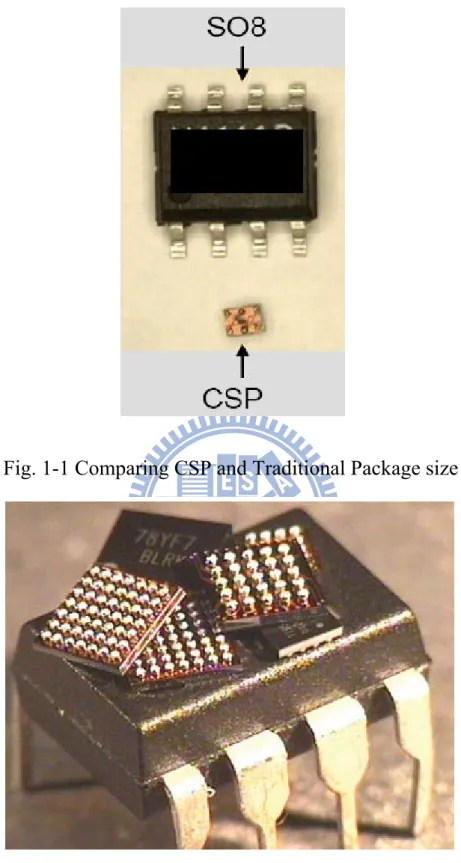
The compact, light weight and multifunctional consumer electronic products, such as notebook, digital camera, cellular phone, or even Global Position System (GPS), are in high demand in modern, technology world. Portable consumer electronic product market areexpending in a light year speeds, and the portability and functionality are crucial factors in the market . As a result , electronic packaging are facing tremendous challenges in reducing not only the size,weight, and the cost of the component, , but also improving the reliability and performance of the devices. To meet these ever-increasing demands for higher levels system integration ,Wafer Level Chip Scale Packaging ( WLCSP ) is the new technology to meet all the needs of the consumers at the same time.
Consolidation of wafer fabrication, packaging and assembly processes is one of the advantages for WLCSP technology. WLCSP is mainly applied to those devices with smaller die size , lower I/O count and larger bump height, and the application of WLCSP products include power IC, analog IC, memory (SRAM, DRAM, flash) and SiP [1.1]. The bare chip must be assembled onto the substrate directly without any protection and encapsulation for WLCSP product. Therefore the reliability performance is a prime challenge. In general, small die size, small
Fig. 1-1 Comparing CSP and Traditional Package size
Fig. 1-2 Comparing CSP and Traditional Package size (2)
chip scale, the package must have an area no greater than 1.2 times that of the die and it must be a single-die, direct surface mountable package. Another criterion often applied to qualify these packages as CSPs is that their ball pitch should be no more than 1 mm .[1.3]
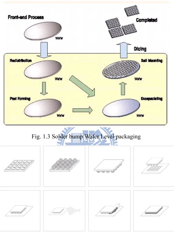
The die may be mounted on an interposer upon which pads or balls are formed, as in flip chip ball grid array (BGA) packaging, or the pads may be etched or printed directly onto the silicon wafer, resulting in a package very close to the size of the silicon die: such a package is called a wafer level chip scale package (WL-CSP) or a wafer level package (WLP). WLP refers to the technology of packaging an integrated circuit at wafer level, instead of the traditional process of assembling the package of each individual unit after wafer dicing. WLP is essentially a true chip-scale packaging (CSP) technology, since the resulting package is practically of the same size as the die . This is the major benefit of CSP packaging . Furthermore, wafer-level packaging paves the way for true integration of wafer fabrication, packaging, test, and burn-in at wafer level, for the ultimate streamlining of the manufacturing process undergone by a device from silicon start to customer shipment. .
Fig. 1.3 Solder bump Wafer Level packaging
1.2 Introduction RDL packing technology
RDL (Re-Distribution Layer) process is developed for the purpose of coordinating IC chip for wire bonding with flip chip assembly. The utilization of dielectric materials and RDL structure will affect the reliability property of solder bump with RDL trace, and we propose to find an optimal approach in this study.
RDL and Bump technology, the most widely-used WLP technology, extends the conventional wafer fabrication process with an additional step that deposits a multi-layer thin-film metal rerouting and interconnection system to each device on the wafer. This is achieved using the same standard photolithography and thin film deposition techniques employed in the device fabrication itself.
Additional level of interconnection redistributes the peripheral bonding pads of each chip to an area array of underbump metal (UBM) pads that are evenly deployed over the chip's surface. The solder balls or bumps used in connecting the device to the application circuit board are subsequently placed over these UBM pads.
Aside from providing the WLP's means of external connection, this redistribution technique also improves chip reliability by allowing the use of larger and more robust balls for interconnection and better thermal management of the device's I/O system.
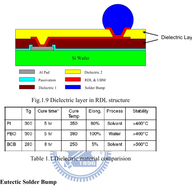
Si Wafer Dielectric 2 RDL & UBM Solder Bump Passivation Dielectric 1 Al Pad
Fig.1.5 Schematic structure of RDL plus solder bump
Comparing with traditional gold wire bonding packaging method, WLCSP has many benefits and the major benefit is chip size package. Currently chips design are mostly peripheral pads originally for gold wire bonding . But we are not willing to Re-design IC’s just only for apply different package method . Re-design include re-make IC fabrication masks , Process fine tune , and Function testing progress , and so on. That’s a huge cost include money and time. Now we can converts peripheral pads to an area array by redistribution layer technology .
RDL Developed by Flip Chip Technologies mainly for pin counts to 150 pins, and with a 0.4mm minimum pitch, the UltraCSP is a flip-chip with a redistribution layer (Figure 1.5) that converts peripheral pads to an area array, and allows die from several suppliers to make parts with a common footprint.
Fig. 1.6 UltraCSP redistribution layer by FCT
1.3 Copper RDL trace
The Copper RDL trace metal are used in this study . The RDL trace , shown in Fig.1.6 : RDL trace are define by 2nd mask PR process after Ti/Copper Sputter process. The wide trace-to-pad connection layout [1.4] is chosen for this study, In this Thesis we also have done experiment to optimize RDL trace thickness .
Fig. 1.7 Copper redistribution layer
RDL trace Peripheral IC
pad for traditional packaging
Fig. 1.8 Layout change to Cu trace at UBM edge
1.4 Dielectric Layer
Di-electric layer in IC packaging is aplied as an electric insulator.When a dielectric material placed in a electric field , electric field charges, causing by dielectric polarization, now flow through the material , but only shift slightly from their average equilibrium positions. The positive and negative charges inside of dielectric will move to two different side of materialto create an internal electric field to partly compensate the external field .[1.5] If the di-electric layer is composed of a weakly bonded molecules , those molecules will not only become polarized , but also reoriented ., and the symmetry axis aligns to the field .[1.6]
Dielectric layer plays an important role in the RDL structure.Not only it plays as the electric insulator of the structure , it also plays a role in the function of high elongation , low modulus , planarizing , high temperature stability , chemically resistant , and alpha particle barrier . As Fig.1.9 shown , RDL layer is placen between two dielectric layers on the wafer .
Si Wafer Dielectric 2 RDL & UBM Solder Bump Passivation Dielectric 1 Al Pad
Fig.1.9 Dielectric layer in RDL structure
Table 1.1 Dielectric material comparision
1.5 Eutectic Solder Bump
Solder is a metal alloy with low melting point. It’s used to join two metal surfaces by alloying ( in molten state ) with their surfaces . Copper , Tin , Gold , Silver Platinum and Palladium are easily soldered , but ickel and brass a bit less so. Cadmium, lead and bronze are still harder. Finally, zinc, steel, and stainless steel are very difficult to solder. Aluminum cannot be soldered with tin-lead alloys, but can be with a barium-aluminum alloy at around 750°F, while continuously scrubbing the surfaces with a stainless steel brush to remove oxide. Only certain aluminum alloys can be "soldered."
The percentage of tin and lead composition in the solder is important. There are several commonly used method to demonstrate this composition. The composition of tin-lead solder is sometimes shown in the form “Sn60”. “Sn” is the chemist’s symbol for tin. This designation means the solder is 60% tin and the rest lead. On the other hand when the alloy designation contains a slash, for example, "60/40", the first number is the percent tin and the second the percent lead.
An important tin/lead solder , called “eutectic,” is 63/73, indicating this alloy goes directly from solid to liquid without a pasty stage. This alloy melts at 361°F (183°C), the lowest melting point of any tin-lead alloy. Other eutectic solders include
• 62.5% tin, 36.1% lead and 1.4% silver (354°F, 179°C)
• 96% tin and 4% silver (430°F, 221°C);
• 97.5% lead and 2.5% silver (581°F, 305°C)
• 0.75% tin, 97.5 % lead and 1.75% silver (590°F, 310°C).
The advantage of a eutectic solder is that it flows very easily. Surface mount components are usually soldered with a eutectic solder. A slightly different alloy, 60/40, provides a thicker coating on wires. [1.7] [1.8]
Fig.1.10 Reflow temperature profile
A typical SMT eutectic solder reflow profile is shown in Figure 1.10 as a reference. The peak temperature at the solder joints should not exceed 220 °C; and the reflow should occur in the next-to-last oven zone to prevent thermal shock and board warping. All Mindspeed BGA packages are qualified. reflow at 225 °C peak temperature per J-STD-020 standard.
Chapter 2
Process detail
2.1 Process flow chart
RDL Process include 4 masks which include 2 Dielectric layers and 2 Photo resists layers , respectively . Following is flow chart (Fig.2.1) illustrates the RDL process in this study .
IQC
Plasma
pretreatment
Gasonic
Dielectric
layer 1
develop
Dielectric
Layer 1
Hard cure
Dielectric
layer 1
Descuum
MATRIX
Ti/Cu
Seed
layer
Sputter
Dielectric
Layer 1
coat
Dielectric
layer 1
Aligner
O2 Plasma
pretreatment
FOI
PR 1
Aligner
PR 1
develop
PR 1
Oven
Cu
teace
Plator
11 um PR 1
Coat , for
RDL Cu trace
PR 1
O2 plasma
Descuum
FOI
Fig.2.1 Process flow chart
PR
strip
Solder
Reflow
Shear
Test
Cu / Ti
Seed layer
Strip
PR 2
Aligner
PR 2
develop
PR 2
Oven
Eutectic
Solder
Plator
35 um PR 2
Coat , for
RDL Cu trace
PR 2
O2 plasma
Descuum
FOI
Cu
UBM
Plator
PR
strip
Dielectric
Layer 2
develop
Dielectric
Layer 2
Hard cure
Dielectric
layer 2
Descuum
MATRIX
Ti/Cu
Seed
layer
Sputter
Dielectric
Layer 2
coat
Dielectric
layer 2
Aligner
Cu / Ti
Seed layer
Strip
2.2 Process steps illustrate
From the flow chart listed below, the side view of each layer formed in each process step illustrated, from wafer to dielectric layer and RDL layer , solder bump formation .
Fig.2.2 Dielectric 1 (PI) coating, UV exposure & developing (Mask 1)
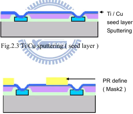
Fig.2.3 Ti/Cu sputtering ( seed layer )
Fig. 2.4 PR coating, UV exposure & developing (Mask 2)
Fig.2.5 Cu plating rerouting trace
PI layer IC Al pad Ti / Cu seed layer Sputtering PR define ( Mask2 )
Fig.2.6 PR stripping & Cu/Ti UBM etching
Fig.2.7 Dielectric 2 (BCB) coating, UV exposure & developing (Mask 3)
Fig.2.8 Ti/Cu sputtering
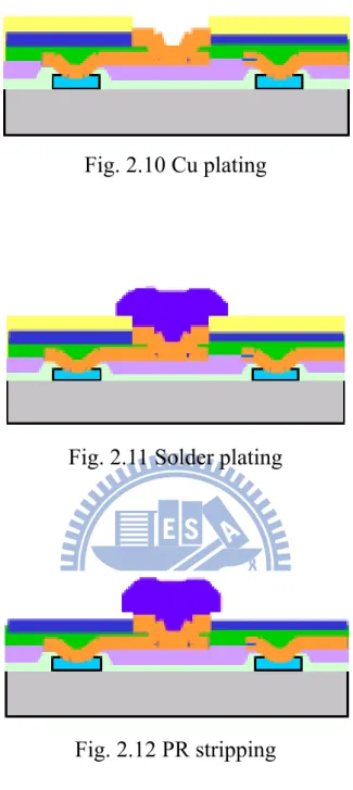
Fig. 2.10 Cu plating
Fig. 2.11 Solder plating
Fig. 2.12 PR stripping
2.3 Process Equipments
Various Process in Photo area , dielectric layer and Photo Resist are processed by different equipments.Following are equipments used in the sequenes of the process flow. (is this what you meant?)
Gasonic plasma : an O2/CF4 plasma pretreatment equipment , used to
remove unknown surface residue of the incoming wafers
Fig.2.15 Gasonic O2/CF4 Plasma Pretreatment
Coater : a spin coater applied inor 4 inch to 8inch wafer process. The device
contains hot plate and cooling plate . The coating thickness of IC is influenced by spin speed , spin time and photo resist dispense quantity . The recipe setting can fully control the thickness condition.
PR / PI / BCB are processed in separate area to prevent cross pollution (or cross-contamintion?).
Fig.2.16 Photo resist coater
UV Aligner: Key equipment of Photo area , for 4 inch to 8inch wafer process.
Has Mask holder and wafer holder . With its CCD image align system and UV light shutter , this device can precisely control the image system and UV intensity .
Dielectric Layer Developer : Basic system structure is similar to spin coater ,
for 4 inch to 8inch wafer process. It also contains hot plate and cooling plate .The difference is in its dispense nozzle and solvent supply system . Solvent will puddle on the wafer , then spin off. The recipe setting can fully control the thickness condition .
Fig2.18 BCB / PI dielectric layer developer
Dielectric Layer Oven : During the dielectric layer curing process , the
chamber must not contain oxygen . This ovenwill pump out air, and purge N2 to avoid dielectric layer surface degrade .
Matrix BCB plasma : After dielectric layer curing process done ,due to the
material’s properity , the via of BCB must have plenty of residue , Matrix plasma contaim Oxygen and Ar , include chemical etch and ion bombard to remove BCB residue .
Fig.2.20 MATRIX BCB plasma
PR Developer : A wet bench develop tank with single cassette that contains
PR developer : A wet bench develop tank . single cassette can contain 25 pcs
wafer immersion once . Developer are THAM+DMSO . (duplicated as well)
Fig.2.22 PR Oven
PR Plasma Descuum : 2 process chamber with 2 cassette loader . O2 plasma
to remove the residue from inside PR opening .
Dage 4000 shear test : It perform bond shear tests in a very controlled and
reproducible way , destructive mode. This allows to characterize the bond and so to optimize the bonding parameters.
Fig.2.24 Dage shear tester
2.4 Material structure comparison
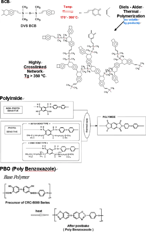
In this chapter, several different Di-electric materials are illustrated and compared, which include BCB , Polyimide , and PBO . The structure of each material is shown as the following Figures demonstrated.
Chapter 3
Device Process and Measurement
In this study , first of all , several predetermined factors need to be decided: Bump structure and the thicknes of the copper RDL layer , the dielectric material layers and adhesion materials between layers.Any parameter chosen here will affect the final result .
3.1 Bump structure study
In this chapter , the bump structure illustrates as Figure 3.1 . Other bump
structure selections will be discuss in the very begining. Four (4) designs of the bump as
1. Si3N4-coated wafer
2. ChipBGA structure: use the masks of ChipBGA product to create four various bump structures .
(1) Bump materials: 63Sn-37Pb (2) Bump height: 150 um (3) Bump size: 230 um (4) UBM size: 220 um
(5) Specification of shear force: 121.3 g
3. Process condition: use current standard RDL process (sputtering Ti(2000 )/Cu(4000 A) UBM, 2 um plating Cu trace, and 8 um plating Cu cap)
Fig.3.1 Dielectric1 coating, UV exposure & developing(Mask 1)
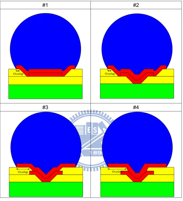
4 types of various UBM structure are prepare to test . as Fig.3.2 shown.
Bump structure #1 #2 #3 #4
Solder bumps sit on Dielectric layer 1
or passivation
Dielectric
Layer 1 Passivation Passivation Passivation Overlap between BCB
#1 #2
Overlap Overlap
#3 #4
Overlap Overlap
Fig.3.4 Bump structure shear test results
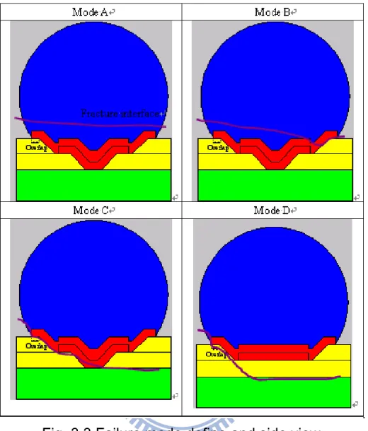
Observations :
(1) The mechanical property of ChipBGA solder bump sitting on the passivation directly is better than that sitting on dielectric layer 1.
(2) The overlap between dielectric layer1and UBM (what is UBM? Don’t remember you mentioned this…)will influence the bump property, and the results sho that a reduction of overlap will have better performance.
(3) We still cannot achieve 100% of failure mode A for the best condition in the study (solder bump sits on passivation and 10 um overlap between dielectric layer1 and UBM).
(4) The shear forces of solder bumps for all structures are above specification but the bumps still may fracture at the interface between dielectric layer1 and passivation.
solder bump for those four bump structures. (5) Other issue
Delamination between dielectric layer1 and passivation may occur after shear test even for failure mode A.
Fig.3.5 Dielectric delamination ( BCB )
3.2 Different structure comparison
1. Structure :
The solder bump is located on the BCB layer ( dielectric layer 1 ) for the original process while it is directly built on the passivation layer for the modified process. Hence almost all weak interfaces, such as
passivation/BCB, BCB/Ti, Cu/BCB, do not exist underneath the solder bump for the modified process.
Mode1
Mode2
Si Wafer
Al Pad Passivation BCB
UBM(Sputtering Ti/Cu + Plating Cu) Solder Bump
Fig.3.6 2 bump site mode – bump sit on passivation and dielectric1
Si Wafer
Al Pad Passivation BCB
UBM(Sputtering Ti/Cu + Plating Cu) Solder Bump
Process Recipe & parameter Pretreatment of passivation layer Cleaning with O2 plasma
Pretreatment of 1st BCB coating Baking at 135 C after AP3000 coating
1st BCB layer Thickness=5 um
1st sputtering Ti/Cu UBM Thickness= 2000 A/2000 A Cu trace (re-routing) Thickness=2 um
Slight compressive stress Pretreatment of 2nd BCB coating Baking at 135 C after AP3000 coating
2nd BCB layer Thickness=5 um 2nd sputtering Ti/Cu UBM
Thickness= 2000 A/4000 A Sputtering TiÎ annealing at 250 C for 5
hoursÎ RF etchingÎ sputtering Ti/Cu Cu cap plating Slight compressive stress
Table 3.1 Process parameter
Fracture interface of solder bump after shear test
Observation :
(1) For mode1 4-mask process, the shear mode of almost all solder bumps is abnormal except few regions .
(2) For mode 2 4-mask process, all solder bumps fracture at the bump for 50 samplings except the marked one, and besides the shear force is above 120 g/bump. (3) The above results exhibit that the bump properties for the mode2 4-mask process is better than that for the original process.
3.3 Effect of Cu trace thickness
Fig.3.8 Experiment result of modify Cu trace thickness
Observations :
(1) The RDL structure with a Cu trace of 2 um thickness has better properties.
of 1 um thickness.
3.4 Annealing condition to Bump property
(1) 250oC for 10 hours (2) 275oC for 10 hours (3) 300oC for 10 hours
(4) 300oC for 10 hours followed by 350oC for 1 hour
Fig.3.9 Bump property vs annealing conditions
Observation :
(1) Shear mode: all annealing conditions belong to the similar shear mode except for 350oC as shown in the following pictures.
Observation :
(1) The adhesion strength of Ti/BCB interface is not good enough regardless of all annealing conditions so this interface usually fractures after shear test. Besides, an extremely high annealing temperature (>350oC) will diminish the strength of the bump structure instead. The fracture between BCB and passivation may occur for 350oC annealing.
(2) The stress of plating Cu film is not a critical issue regarding the bump property because the tensile stress of plating Cu film will release during storage at room temperature.
(3) The above results exhibit that an annealing treatment cannot resolve the adhesion problem between BCB and Ti entirely.
Observation :
The Cu land size on PI layer (126 um) and BCB bottom opening (96 um) are much larger than the fracture area (~30 um).
(1) The bump/RDL structure of four corner bumps is different from that of four central bumps while the structure of four central bumps is the same including Cu land size on PI layer and BCB opening.
(2) The stress underneath central bumps might be larger than that of corner bumps because of complex structure in localized region.
(3) The passivation and circuit layers underneath bump #2 are peeled off after processing of bump/RDL structure, and it looks to be related to stress issue from the fracture mode. The strss might form during BCB curing or/and reflow processes.
(4) The shear mode and the shear force are within specification for both ChipBGA structures.
(5) For the bump sitting on the first PI layer, the shear mode of all solder bumps belongs to mode B (fracture at the bump after shear test) and the shear force is 110~130 g/bump.
(6) In terms of the bump property at wafer level, structure #1 looks a bit better than structure #2 but they have no much difference. Hence the board level property is essential to determine the optimal ChipBGA structure
(7) The fracture of the passivation/dielectric interface does not happen when PI is used as the first dielectric layer for two ChipBGA structures, and it implies that PI layer can offer superior stress buffer effect.
3.6 Various dielectric layer material experiment
ChipBGA structure:
(1) Thickness of dielectric layer 1 : 4~5 um (2) Thickness of dielectric layer 2 : 4~5 um (3) Thickness of Cu RDL: 2 um
(4) Thickness of Cu cap underneath the bump: 8 um (5) Bump height: 150 um
Dielectric layer are BCB , Polyimide A , Polyimide B , Polyimide C , and PBO . totally 5 dielectric materials and 9 combinations as Table 3.2 shown , same with previous experience , all combination trial 2 types of bump structure . as Fig.3.12
Fig. 3.15 Various dielectric layer
Observation: ( fracture mode please refer to Fig. 3.3 )
(1) The shear mode and the shear force are within specification for both ChipBGA structures.
(2) For the bump sitting on the first PI layer, the shear mode of all solder bumps belongs to mode B (fracture at the bump after shear test) and the shear force is 110~130 g/bump.
(3) For the bump sitting on the passivation layer, 70% of solder bumps belong to mode B while 30% are mode C (fracture at the bump as well as the BCB/UBM interface after shear test). The shear force of the solder bump is 110~130 g/bump too.
essential to determine the optimal ChipBGA structure
(5) The fracture of the passivation/dielectric interface does not happen when PI is used as the first dielectric layer for two ChipBGA structures, and it implies that PI layer can offer superior stress buffer effect.
Chapter 4
Results and Discussion
4.1 Final Result of RDL study
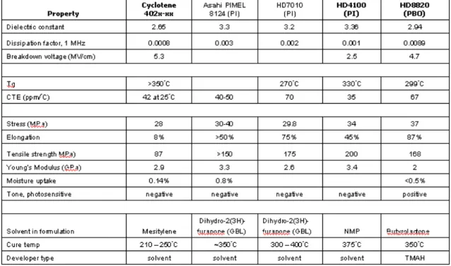
The utilization of dielectrics materials will affect not only the mechanical property of RDL structure but also the reliability performance. Because two dielectric layers are used in RDL structure, the adhesion between two dielectric layers is also critical. In this study, we utilize five kinds of dielectrics layers (BCB, polyimide and PBO) and a total of nine (9) combination series
Table 4.1 shows the bump shear test result of each condition after bumping, TCT and PCT at wafer level. The corresponding shear modes of “pass” and “fail” are shown on Figure 2 (do you want to relable the figure? Like 4.2?)and normally the bump must be fractured in the solder material after shear test. Those wafers receive TCT for 500 cycles from -65C to 150C (referring to MIL-STD-883D 1010.7) and PCT for 168 hours at 121C and RH100% (referring to JESD22-A102-B), andthe result demonstrates that not all of polyimide materials are compatible with BCB and not all of dielectric materials can be applied to RDL structure. Because BCB material has superior moisture-uptake resistance and lower dielectric constant, we choose BCB as the top dielectric layer and polyimide C as the bottom dielectric layer (combination 8). A WLCSP chip with this RDL structure is further confirmed to pass both TCT (-55C to 125C for 1000 cycles) and HTS (150C for 1000 hours) tests at board level when the die size is smaller than 3 mm by 3 mm.
bump structure on the mechanical property of the rerouted bump. In this study, the effects of the overlap between UBM and BCB opening and the sitting location of the rerouted bump are studied. Figure 4.3 shows two different bump structures utilized for this experiment. Our conclusion is the solder bump sits on PI layer has better performance than that sits on passivation. A small overlap between UBM and BCB opening benefits the integrity of the solder bump when the bump is located on passivation. We believe the effect of overlap between UBM and BCB opening will be insignificant for the bump sitting on PI layer though we do not cover this result in this study.
The coverage of dielectric layer on the dicing street will also affect the bump integrity because of stress issue. We discover that the stress accumulated in the die and the wafer warpage resulting from the full coverage of dielectric layer on the street will cause bump fracture after shear test. To open the dielectric layer on the street is more recommended for RDL structure.
The adhesion between two dielectric layers is very critical to the RDL structure. In this study, different plasma treatment methods were applied to enhance the adhesion between PI and BCB, including Ar plasma and O2 plasma. The conclusion is that the plasma treatment is required but there is no difference between Ar plasma and O2 plasma. Actually, both Ar plasma and O2 plasma pass the final reliability test. In addition, the baking treatment right before BCB coating onto PI is also essential because PI material might absorb the humidity during RDL process, especially for wet etching process. Otherwise, the adhesion between PI and BCB might be degraded and will damage the RDL structure.
Fig.4.1 Final Product
Chapter 5
Conclusion
A robust RDL structure (PI/Cu trace/BCB) for WLCSP application is performed in this study, and this structure passes both wafer-level and board-level reliability tests, including TCT for 1000 cycles from -55C to 125C. The utilization and the compatibility of dielectric materials are crucial to the bump integrity. The solder bump sits on PI layer has better performance when we utilize PI as the first dielectric layer and BCB as the top one. It would be recommended to keep the dicing street free of the dielectric layer in view of stress and wafer warpage issues. The surface treatment between PI and BCB is also required in order to enhance the adhesion between these two dielectric materials.
References
[1.1] J. H. Lau, Low Cost Flip Chip Technologies for DCA, WLCSP and PBGA Assemblies, McGraw-Hill, New York, 2000.
[1.2] P. Garrou, “Wafer-level packaging has arrived”, Semiconductor International, October 2000, p. 119-128.
[1.3] The Nordic Electronics Packaging Guideline, Chapter D: Chip Scale Packaging
[1.4] IMAPS 2008 conference paper “ A Novel Repassivation/RDL CSP Technology for Minimizing Parasitic Elements in ASIP Products ‘’ P23
[1.5] Classical Electrodynamics,John David Jackson Published by Wiley,1998 ISBN7130932X,780471309321
[1.6 ] J. Daintith (1994). Biographical Encyclopedia of Scientists. CRC Press. p. 943. ISBN 0750302879.
[1.7] Clifford L. Barber. Solder. Its Fundamentals and Usage. 2nd Ed. Chicago: Kester Solder Company, 1961.
[1.8] National Aeronautics and Space Administration. Office of Technology Utilization. Soldering Electrical Connections. A Handbook. 4th edition. NASA SP-5002.Washington, D.C.: U. S. Gov't Printing Office , 1967.