以氫化物氣相磊晶法開發氮化鎵基板研究
187
0
0
全文
(2) 以氫化物氣相磊晶法開發氮化鎵基板研究 Study of GaN Substrates Developed by Hydride Vapor Phase Epitaxy 研 究 生: 黃 信 雄. Student:Hsin-Hsiung Huang. 指導教授: 李 威 儀. Advisor:Dr. Wei-I Lee. 國立交通大學 電子物理研究所 博士論文 A Thesis Submitted to Department of Electrophysics College of Science National Chiao Tung University in partial Fulfillment of the Requirements for the Degree of Doctor of Philosophy in Electrophysics September 2008 Hsinchu, Taiwan, Republic of China. 中華民國. 九十七 年 九 月.
(3) 以氫化物氣相磊晶法開發氮化鎵基板研究 研 究 生: 黃 信 雄. 指導教授: 李 威 儀. 國立交通大學電子物理研究所 中文摘要 由於缺乏晶格匹配的基板,三族氮化物元件只能採用異質磊晶的方式,利 用晶格常數不同的材料來當作基板,因此有缺陷密度過高,以及因為熱膨脹 係數不同造成晶體彎曲甚至破裂的問題。對於低電流密度的元件(例如 LED) ,這些問題的影響不大,但是對於高電流密度元件(例如藍光 LD) 、高 功率元件或 UV 元件而言,影響就相當可觀,若有單晶三族氮化物基板來進行 同質磊晶,不但可以降低晶格常數不匹配所造成的缺陷密度、熱膨脹係數不 同所造成的彎曲;更可大幅簡化元件的製程及提昇元件的可靠度。未來在光 電元件產業的發展上,單晶三族氮化物基板必然具有舉足輕重的地位。對於 國內學術界而言,若有單晶三族氮化物基板(GaN、AlN 等)作為研究基礎, 在相關領域的研究上等於直接躍遷至不同的競爭平台上。 本論文的研究方向在於使用氫化物氣相磊晶法成長氮化鎵厚膜,其中最大的問 題在於如何克服因熱膨脹係數不同所產生的熱應力所導致的晶片破裂,我們運用 了一些 ELOG 所衍生的方法及溫度梯度成長方法來克服應力的問題,並獲得良 好的成效。經由氫化物氣相磊晶所成長的厚膜再利用雷射剝離的方法將厚膜從原 生基板上分開,而得到獨立氮化鎵基板。我們分別使用了掃描式電子顯微鏡,陰 極螢光,光致螢光,拉曼光譜,霍爾量測,高解析 X 光,原子力顯微鏡,微分 干涉差光學顯微鏡等工具來量測氮化鎵基板的特性。除此之外,以氫化物氣相磊. i.
(4) 晶所成長的氮化鎵化學特性也經由濕式化學蝕刻法加以研究,其不同晶面的活化 能也分別經由實驗值計算出來。 總之,厚度超過 300 微米的透明氮化鎵厚膜已經開發出來,其差排密度大約介 於 106 到 107cm-2 之間,霍爾電阻大約是 0.09 Ω-cm,未摻雜的載子濃度大約是 1.6x1017 cm-3,X 光搖擺曲線的半高寬大約是 150 秒。在成長厚度增加以及磊晶 條件最佳化後,這些特性都可以再改善。 單晶三族氮化物基板將是推動下一代三族氮化物元件發展的關鍵載具,希 望經由本論文研究計劃後,未來可以穩定提供高品質的單晶三族氮化物基板 給其他學界單位進行研究使用,以對國內的光電發展盡一份心力。. ii.
(5) Study of GaN Substrates Developed by Hydride Vapor Phase Epitaxy. Student:Hsin-Hsiung Huang. Advisor:Dr. Wei-I Lee. Department of Electrophysics National Chiao Tung University. Abstract Due to the lack of lattice-matched substrates, current nitride base devices are mainly hetero-epitaxially grown on lattice mismatched substrates. The large mismatches in lattice constants between substrates and epitaxial films cause high defects densities. Furthermore, differences in thermal expansion coefficients between substrates and epitaxial films induce large warpage or bowing of the epi-layers. While these disadvantages may not limit the performance of low current density devices, such as LEDs, they will certainly severely affect high current density devices, such as blue laser diodes and high power electronic devices. The availability of freestanding GaN substrates will provide the overgrown GaN epi-layers the advantages of reduced defects, less bowing, improved reliability, as well as greatly simplified device process afterwards. It is believed that free-standing nitride substrates will play vital roles in the next stage of GaN and InAlGaN devices development. In this thesis, we used the HVPE system to study the GaN wafer fabrication.. iii.
(6) Several methods for preventing the crack of GaN thick-film during the HVPE epitaxy process were used in this thesis, including the epitaxial lateral overgrowth, air-bridged, dot air-bridged, and temperature ramping technique. These methods can effectively preventing the crack of GaN thick-film in HVPE growth process. After the GaN thick-film prepared, the laser lift-off technique was used to separate the GaN thick-film from original substrate. The freestanding GaN thick-film was obtained after these processes. The characteristics of freestanding GaN were analysised by SEM, CL, Raman spectroscopy, PL, Hall measurement, HRXRD, AFM, and Normaski OM. Furthermore, the chemical properties of HVPE GaN were also studied by wet chemical etching. The activation energy was calculated of different crystal facets of GaN. Overall, the thickness more than 300 μm freestanding GaN was obtained by these strain reduced methods. The color is transparent and the dislocation density is in the range of 106 to 107 cm-2. The resistivity is about 0.09 Ω-cm. The undoped carrier concentration is about 1.6x1017 cm-3. The FWHM of HRXRD rocking curve is about 150 aresec. The performance can be improved after increasing the thickness and optimizing the growth conditions. The project of this thesis is dedicated to provide free-standing nitride substrates to other researchers in Taiwan in the future. It is hoped that we can hence provide a major new vehicle for our domestic research on nitride devices.. iv.
(7) 誌. 謝. 從進入交大唸博士班,很快的已經過了四年又一個月了,在這段時間嘗試了 很多人生中的第一次:第一次在國際會議上站上台用英文報告、第一次投稿期刊 論文、第一次寫專利、第一次寫大型計劃、第一次修全部用英文授課及討論的課 程、第一次實驗室全體出動烤肉,第一次到大山背看螢火蟲……等等,有太多第 一次的經驗可以回味,可以感動。 在這段期間首先要感謝李威儀老師全力的支持和指導,老師開放的指導方式可 以使學生養成獨立思考的能力,還記得第一次到老師辦公室門口時,看到的博士 學位與加拿大雁的故事,印象很深刻。其次要感謝碩士班的指導教授-杜立偉老 師,在碩士班期間被訓練成的嚴謹做事態度,至今依然受用,也感謝杜老師在博 士班期間量測設備上的支持。再來要感謝的是實驗室的博士班同學-豐格,雖然 沒有一起畢業,但我還記得一起修課,一起考試的回憶,相信你的選擇對你的人 生是正確的,祝福你。博士班學弟奎銘,你的加入讓我更無後顧之憂,可以放手 進行更多的實驗構想,加油!下一個畢業的一定是你。還有在台大光電博士班的 學弟虹諭,你的數據讓我的第一篇期刊論文順利誕生。碩班學弟妹,廷立、佩倫、 宏瑋,你們對實驗室現有機台的架設幫忙很多。還有振豪,你的加入讓我們在 MOCVD 上有強力的後援。還有其他碩士班的學弟妹,怡麟、子強、彥偉、溫壬、 柄均、源根、文謙、治華、仲山、凱翔、偉誠、定儒,以及新加入的博士班生力 軍-彥顯、尹豪,你們使我的領導規劃能力以及人生的體驗有更長足的進步。. v.
(8) 還有工研院的蔡政達經理蔡董,感謝您給我機會可以進入工研院,開拓了更高 的視野,劉柏均博士的共同討論,使我的經驗更加茁壯,郭義德郭大哥,主立、 志銘、東煒,郁香姐,以及小媽瑞琴姐,還有許多工研院的伙伴,你們也都使我 的實驗經驗受益良多。 再來要深深感謝的是我的父親-黃華山先生以及母親-丁麗敏女士,你們無怨 無誨的付出,才有今天的我。還有我的兩位妹妹郁文、及郁惠,感謝妳們在我求 學期間較沒有經驗能力時對父母親全心全力的照顧,使我可以安心求學,沒有後 顧之憂,再來的責任就交給我吧! 還有我的未婚妻-妮婉,沒有妳的溫柔的全力支持,我沒辦法這麼快拿到學 位。還有家中的阿貓阿狗-吉米、小藍波、Angel、皮蛋,你們在主人心情苦悶 時總是不離不棄的陪在我身邊,讓我搔小肚肚,安慰主人的心。 套用陳之藩先生的一句話,要感謝的人太多了!那就謝天吧!. vi.
(9) Contents Chinese Abstract…………………………………………………………..……………i English Abstract…………………….………………………………………………...iii Acknowledge………………………………………………………………………….v Contents…………………………………………………………………….………vii Tablet Contents...............................................................................................................x Figure Contents…………………………………………………..…….……………..xi. Chapter 1 1.1. Introduction…………………………………………………..………1. History of Gallium Nitride Base Optoelectronic Devices and Properties……….………………………………………………………….1 1.1.1 History of GaN Devices……………….…………………………..1 1.1.2. 1.2. Structure and Properties of GaN…………….…………………….3. Introduction to Hydride Vapor Phase Epitaxy Technique………………….4. 1.3 Effect of Strain in Gallium Nitride…………………………………….…...8. 1.4. 1.3.1. Calculation of strain in GaN Epitaxy Film…….…………...……...8. 1.3.2. Effect of Emission in GaN on Strain………………………..….10. 1.3.3. Strain and Raman Spectrum in GaN……………………………..13. References……….………………………………………………….…..16. vii.
(10) Chapter 2 2.1. Air-bridged Epitaxial Lateral Overgrowth......................................47. High-Void Air-Bridged Technique………………………………………..47 2.1.1 Introduction of Air-Bridged Technique………………….……….47 2.1.2. Experiment……………………………………………………….49. 2.1.3. Result and Discussion……………………………………………50. 2.1.4. Conclusion………………………………………………………..54. 2.2 Strain reduced GaN thick film grown by hydride vapor phase epitaxy utilizing dot air-bridged structure………………………………………...54. 2.3. 2.2.1. Introduction………………………………………………………55. 2.2.2. Experiment……………………………………………………….56. 2.2.3. Result and Discussion……………………………………………57. 2.2.4. Conclusion………………………………………………………..60. References…………………………………………………………….…..62. Chapter 3. Using Temperature Ramping Technique to Grow Crack-Free GaN Thick-Film by Hydride Vapor Phase Epitaxy…………..…..77. 3.1. Introduction……………………………………………………………….77. 3.2. Experiment……………………………………………………….……….78. 3.3. Result and Discussion………………………………………….…………79. 3.4. Conclusion………………………………………………………………..83. viii.
(11) 3.5. References………………………………………………………………..84. Chapter 4. Introduction to Laser Lift-off…………………..………………….94. 4.1. Introduction to Laser Lift-Off Technique…………………..……………..94. 4.2. Laser Lift-Off System……………………………………………….…….97. 4.3. Results and Discussion………………………………………………..…..99. 4.4. References……………………………………………………………….103. Chapter 5. Extended Micro-tunnels in GaN Prepared by Wet Chemical Etch………………………………………………………………...118. 5.1. Introduction……………………………………………………………..118. 5.2. Experiment……………………………………………………….……..120. 5.3. Result and Discussion………………………………………….………..121. 5.4. Conclusion……………………………………………………………....127. 5.5. References……………………………………………………………….129. Chapter 6. Conclusion…………………………………………………….…...144. Appendix A……………………………………………...………………………...148 Publication List………………………………………...…...……………………...164. ix.
(12) Tablet Contents Tab. 1-1. The properties of gallium nitride………………………………………….28. Tab. 1-2. The methods of bulk GaN growth………………………………………...34. Tab. 1-3. Raman selection rule for optical phonon in wurtzite structure…………...44. Tab. 1-4. Familiar Raman phonon frequency values in wurtzite structure of GaN…45. Tab. 1-5. Raman calibration factor………………………………………………….46. Tab. 2-1. Thermal expansion coefficient of wurtzite crystal………….……….……76. Tab. 3-1 The properties of GaN wafer of NOD Lab……………………………….93 Tab. 4-1. The Comparsion of Nd:YAG and excimer KrF lasers…………………..115. Tab. 5-1. Dangling bonds and surface energy of GaN facets……………………...142. x.
(13) Figure Contents Fig. 1-1. The applications of nitride base optoelectronic devices………………..23. Fig. 1-2. The optimum transform efficiency of different material in visible Region…………..………………………………………………………24. Fig. 1-3. The evolution of solid state lighting from 1920………..………………..25. Fig. 1-4. The relationship of lattice constant and energy gap of different compound semiconductors……………..……………………………….26. Fig. 1-5. The clinographic projection of the wurtzite structure of GaN. The c and a are the lattice constant…………………….……………………...27. Fig. 1-6. The phase diagram of GaN…………………………..…………………..31. Fig. 1-7. The sketch of HVPE system……………………………..………………32. Fig. 1-8. The reactor of HVPE system…………………………..………………...33. Fig. 1-9. The growth model in vapor phase epitaxy of GaN……………..………..35. Fig. 1-10 Equilibrium partial pressures of gaseous species inside the reactor……..38 Fig. 1-11 The Stress distribution in thick-film with substrate……………………...39 Fig. 1-12 The Band structures and respective transition in GaN…………………..40 Fig. 1-13 Strain dependence of the free exciton resonance energies in wurtzite GaN………………………….…………………………………………41 Fig. 1-14 The scheme of Raman and Reyleigh scattering………………………….42. xi.
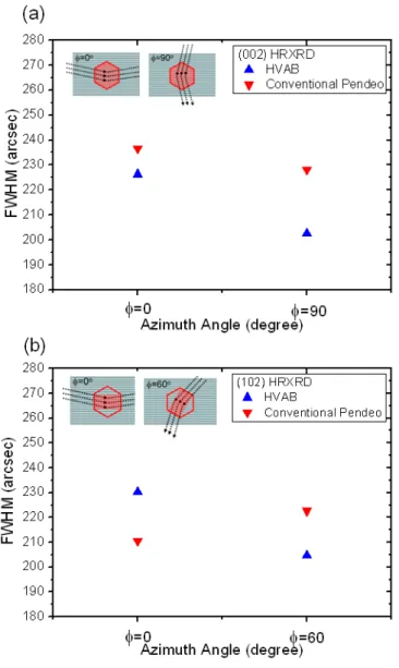
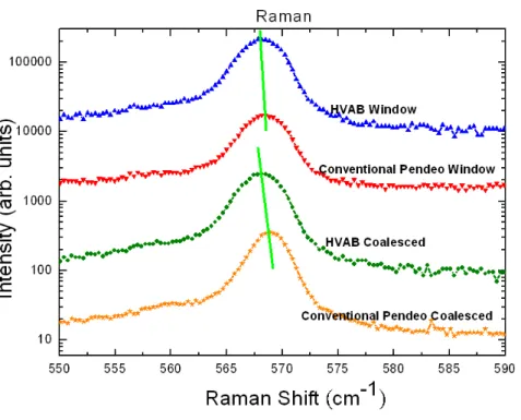
(14) Fig. 1-15 Optical phonon modes in wurtzite structure crystal……………………..43 Fig. 2-1. Schematics and SEM images of the conventional pendeo and the HVAB structures after HVPE regrowth…………………..…………….65. Fig. 2-2. Plane and cross-sectional CL images of the conventional pendeo and the HVAB structures………………………..……………..……………66. Fig. 2-3. Schematics of growth mechanism and SEM images of initial state of the HVPE regrowth in the conventional pendeo structure and the HVAB structures………………………………………..………………67. Fig. 2-4. Azimuthal dependence of the FWHM of GaN (002) and (102) HRXRD rocking curve of the conventional pendeo and the HVAB structures......68. Fig. 2-5. Reciprocal space maps around the (002) point of c-plane GaN grown by HVPE…………………………………………………..…………….69. Fig. 2-6. Raman spectra of E2(high) phonon frequency of the conventional pendeo and the HVAB structure……….……………………………….70. Fig. 2-7. Schematic of the GaN thick-film fabrication process with the dot air-bridged structure by HVPE………………………………………….71. Fig. 2-8. SEM image of the dot air-bridged structure…………..…………………72. Fig. 2-9. The CL image of GaN thick-film of the dot air-bridged structure……....73. Fig. 2-10 CL image and Raman spectra of the dot air-bridged Sample........………74. xii.
(15) Fig. 2-11 Photography of a 300 μm GaN thick-film in 1.5-inch diameter on 2-inch sapphire substrate without any crack………………..………..…75 Fig. 3-1. Schematic of the temperature ramping GaN growth by HVPE……….....86. Fig. 3-2. A 1.5 inch, 300 μm crack free GaN thick-film grown on sapphire substrate with temperature ramping step………………………………..87. Fig. 3-3. The cross-sectional CL images of temperature ramping layer at various ramping rate……………..……………………………………...88. Fig. 3-4. The CL and Raman spectra of cross-sectional regions of the sample with 1.0oC/min ramping rate………………………...……………………….89. Fig. 3-5. The rocking curve of HRXRD and CL image of the freestanding GaN with 1.0 oC/min ramping rate………………………………………….90. Fig. 3-6. A 2 inch, 360 μm-thick GaN on sapphire substrate before and after LLO Process……………………………………………………….………….91. Fig. 3-7. The CL image of a regrown 600 μm GaN thick-film……………………92. Fig. 4-1. The laser-lift-off process sketch………………………………..……….105. Fig. 4-2. The thermally induced decomposition of nitride semiconductors using a heating rate of 0.3 K/s……………………………..…………………106. Fig. 4-3. The relation of decomposition depth caused by a single pulse and absorbed pulse intensity of the Nd:YAG laser………………..……….107. xiii.
(16) Fig. 4-4. The sketch of the laser lift-off system………..………………………108. Fig. 4-5. The SEM images of the backside of GaN films after LLO process..…..109. Fig. 4-6. The plane view Raman spectra of GaN thick-film before and after LLO Process…………………………………………………………………110. Fig. 4-7. The cross sectional Raman spectra of GaN thick-film before and after LLO process…………………………………………………………...111. Fig. 4-8. The XRD rocking curve of GaN thick-film before and after LLO Process…………………………………………………………………112. Fig. 4-9. The SEM images of GaN thick-film after LLO process in air ambient and nitrogen ambient…………………………………………………..113. Fig. 4-10. The experimentally determined epitaxial layer thickness as a function of diameter for fabrication complete GaN wafers……………………114. Fig. 4-11. The temporal and spatial variation of the temperature at GaN/sapphire interface……………..………………………………………………..116. Fig. 4-12. The beam profile of excimer 248 nm KrF and 355 nm Nd:YAG Lasers………………………..…………………………..…………....117. Fig. 5-1. Cross sectional structure of the GaN sample prepared for chemical etch…………………………………………………...………………..132. Fig. 5-2. Optical microscopic image of GaN EMTs after 30 minutes’ etch in. xiv.
(17) molten KOH at 250 oC…………………………..…………………….133 Fig. 5-3. Cross sectional SEM images of GaN EMT along the < 1 100 > direction at different temperatures…………………..…………………………...134. Fig. 5-4. Cross-sectional SEM images of GaN EMTs along the < 1120 > direction at different temperatures………………….…………………………...135. Fig. 5-5. The bird-view cross-sectional SEM images of EMTs along the < 1120 > direction and the insert along the < 1 100 > directions……………….136. Fig. 5-6. SEM images of cross section of GaN after the wet chemical etching with different directions……………………………………………………..137. Fig. 5-7. Plot of the depth of GaN tunnels in different directions…………..……138. Fig. 5-8. Time-dependence of the etching depth of GaN tunnels at various Temperatures…………………………………………………………..139. Fig. 5-9. Cross sectional structure of GaN EMTs, beginning to form well-shaped triangular tunnels and forming larger triangular tunnels upon facet etching…………………………………………………………………140. Fig. 5-10. Arrhenius plot of etching rates of two crystal facets of GaN…..……..141. xv.
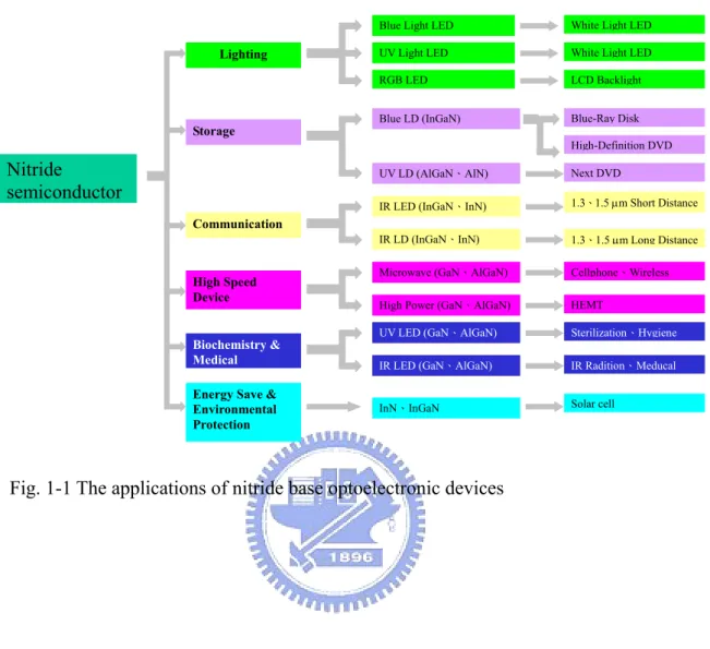
(18) Chapter 1. Introduction 1.1 History of Gallium Nitride Based Optoelectronic Devices and Properties. 1.1.1 History of GaN Devices Nitride alloys (InN, GaN, AlN) represent the most promising class of optoelectronic materials, as shown in Fig. 1-1. The binaries and their alloys are direct bandgap semiconductors whose energy gaps cover the spectral region from the infrared to deep ultra violet. Nitride devices such as light emitting diodes, field effect transistors and laser diodes have various applications in traffic lights, full color displays, and LCD backlight among others. Most of these applications are based on GaN material and its alloys. GaN material had been investigated for more than 60 years. However, due to the leak of a suitable substrate, the quality of GaN crystal remained poor until the 90s. In 1940, Juza and Hahn synthesized GaN from ammonia gas and hot gallium. This method produced only small needles and platelets. In 1969, Maruska and Tietjen employed chemical vapor deposition to make a large-area layer of GaN on sapphire substrate. In 1983, Yoshida et al. deposited a GaN layer at high temperature AlN buffer layer on sapphire substrate. Akasaki et al. first deposited a low-temperature (LT, approximately 600 oC) AlN buffer layer on sapphire substrate by metal-organic chemical vapor deposition (MOCVD). Then, they grew a high-quality mirror-like GaN after subsequent high temperature (rough 1000 oC) with an LT AlN buffer layer. In 1991, Nakamura et al. of Nichia Corp replaced the LT AlN buffer layer with an LT 1.
(19) GaN buffer layer to form a high-quality mirror-like GaN. Another problem associated with GaN devices is the difficulty of obtaining p-type doped GaN. This problem was first solved in 1989 by Akasaki et al., who used the Cp2Mg as the source of doping Mg ions in GaN during the growth process, and then employed low-energy electron beam irradiation (LEEBI) to scan the samples to yield p-type GaN. In 1992, Nakamura et al. found that an electron beam annealed the sample, breaking the Mg-H bonds. Annealing GaN:Mg at over 750 oC in N2 or in a vacuum yielded the same results. All recent works have produced high-brightness visible LEDs, which are available today, and are especially contributed in the blue ray region. In 1995, Nakamura et al. announced the fabrication of a high-quality green LED with InGaN quantum wells (QW) structure as the active layer.[2] It outperformed the blue-green LED whose active layer was fabricated with the double-heterostructure. The color of light of the QW LED can be changed from blue to yellow by changing the In content in InGaN QW. As the In content in InGaN QW increases, the ray color from the LED is shifted from blue to yellow. As the composition of In in InGaN increases, the quality of InGaN decreases. The intensity of InGaN QW LED decreases as the In content in InGaN increases. However, the human eye is more sensitive to green light than to blue light, as shown in Fig 1-2. Even though the intensity of the green LED is less than that of the blue LED, the green LED is brighter than blue LED for human eyes. The brightness of GaN LED increased very much in recent years. Figure 1-3 shows the evolution of lighting. In the future, nitride-based LEDs will be mainstream lighting. Before 1996, most research groups utilized optical pumping technique to make the GaN laser diodes (LD). In 1996, Nakamura et al. of Nichia Corp. first reported a. 2.
(20) GaN LD that could operate at room temperature. In the early stage of GaN LD development, the GaN LD was pulse-resonant, rather than continuously wave-lasing. In Dec. 1996, Nichia Corp. announced a continuous wave GaN LD, fabricated on c-plane sapphire substrate with an etched mirror facet. However, its lifetime was only 1s, which was too short for use in any application. The last two decades have seen the extensive development of the GaN LD. A GaN LD with a lifetime of more than 10000 h has been developed and commercialized.. 1.1.2 Structure and Properties of GaN The III-A group elements, B, Al, Ga and In can form the compounds with N, with the composition AIIIN as shown in Fig. 1-4. Most of the chemical bonds in these III-V compounds are covalent, with tetrahedral bonds at each atom. The GaN and its related III-V compounds can crystallize into the following three crystal structures: (1) zincblende, (2) wurtzite and (3) rock salt structures. However, under ambient conditions, the wurtzite structure is the more common thermodynamically stable phase. The rock salt structural phase transition takes place at high pressure, and the zincblende structure is a metastable. The zincblende and wurtzite structures are very closely related crystallographically. The bonds in zincblende and wurtzite are all tetrahedral. The Bravais lattice of the wurtzite structure is hexagonal and the c-axis is as perpendicularly to the hexagon. In the zincblende structures, the stacking layer is. GaANAGaBNBGaCNCGaANAGaBNBGaCNCGaANAGaBNBGaCNC……. While for the wurtzite structure, it is. 3.
(21) GaANAGaBNBGaANAGaBNBGaANAGaBNBGaANAGaBNBGaANA……. Figure 1-5 shows the clinographic projection of the wurtzite structure of GaN. The space group of the wurtzite structure is C46V (P63mc). It has two lattice parameters a and c in the ratio c/a = 8 = 1.633, as shown in Fig. 1-5. The wurtzite structure 3 consists of two hexagonal close-packed (hcp) sublattices with a shift of u = 3/8 in fractional coordinates along the c axis. Every Ga (N) atom is surrounded by four N (Ga) atoms, which are arranged on the edges of a tetrahedron. The two inequivalent atomic positions are ( 1 , 2 , 0) and ( 1 , 2 , u ) , such that Ga atoms are at both 3 3 3 3. (0, 0, 0) and ( 1 , 2 , 1 ) , while N atoms at (0, 0, u ) and ( 1 , 2 , 1 + u ) . Yeh 3 3 2 3 3 2 et al. defined two slightly different bond lengths,[3] Re(1) = u × c. E(1-1). and Re(2) = a × [1/ 3 + (1/ 2 − u ) 2 × (c / a ) 2 ]. E(1-2). where u is the dimensionless internal structure parameter. Re(1) equals Re(2) for an ideal wurtzite structure. Table 1-1 presents the other properties of GaN.. 1.2 Introduction to Hydride Vapor Phase Epitaxy. The Hydride Vapor Phase Epitaxy (HVPE) technique was developed more than 30 years ago to grow GaP and GaAsP light emitting diodes (LEDs).[54] The HVPE technique was also applied to grow GaN-based devices. However, for the following. 4.
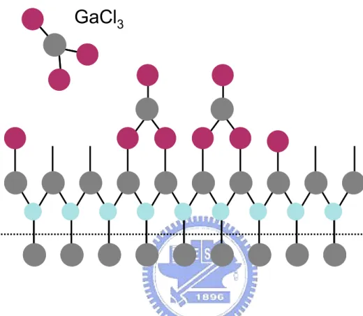
(22) reasons, in the 80s, the attempt to use the HVPE technique to grow GaN was almost abandoned. 1、The leak of a suitable substrate for the homo-epitaxial growth of a GaN device and the large defect density make the quality of GaN devices uncontrollable. 2、The high growth rate of HVPE makes it unfavorable for growing GaN devices. 3、The p-type doping of GaN by HVPE is difficult.[55] However, the high growth rate of GaN by HVPE can be exploited to produce GaN substrate. In the ‘90s, the focus of the application of HVPE shifted to the fabrication of a GaN substrate.[56,57]. The GaN substrate cannot be produced by conventional pulling-process synthetics because of the decomposition temperature of GaN is lower than its melting temperature, as shown in Fig. 1-6.[58] Several techniques have been used to prepare the GaN substrate, as shown in Tab. 1-2. In these techniques, HVPE is the most suitable method for preparing high-quality GaN substrates because it supports a high growth rate, and produces no impurity from such organic sources TMGa. In recent years, for reducing defect density including epitaxy lateral overgrowth (ELOG), pendeo and air-bridged techniques have been developed and combined with the HVPE technique for preparing GaN substrate.[59-62] High-quality GaN substrates can be obtained by combining of these techniques. Figure 1-7 shows an HVPE system. The system consists of several sub-systems, including: a mass flow control system, an oven system, a pressure control system, an exhaust system and others. Figure 1-8 presents the concept that underlies the HVPE reactor. For HVPE GaN growth, the GaClx and ammonia gases (NH3) are used as Ga and nitrogen sources, respectively. GaClx is generated by a reaction of gaseous HCl and Ga metal at 850 oC. It is then transported into the growth zone with a carrier gas to react with NH3 gas. The reaction of GaClx and NH3 yields the GaN crystal in the. 5.
(23) growth zone. Cadoret et. al. developed a theoretical model to explain to the growth mechanism of bulk GaN in HVPE.[63-69] The reactions are as follows.. Adsorption of NH3 molecules ZZX NH 3 V + NH 3( g ) YZZ. (R1). Adsorption of N atoms by NH3 decomposition ZZX 2 N + 3H 2( g ) 2 NH 3 YZZ. (R2). Adsorption of GaCl molecules on N atoms. ZZX NGaCl N + GaCl( g ) YZZ. (R3). where the subscript “g” refers to gaseous species, and “V” is denotes a vacant site. Two chlorine desorption mechanisms are considered. H2 and chlorine desorption mechanism:. ZZX 2 NGa − ClH 2 NGaCl + H 2( g ) YZZ ZZX NGa + HCl( g ) NGa − ClH YZZ. (R4) (R5). GaCl3 and chlorine desorption mechanism:. ZZX 2 NGa − GaCl3 2 NGaCl + GaCl( g ) YZZ. (R6). ZZX 2 NGa + GaCl3( g ) 2 NGa − GaCl3 YZZ. (R7). The two overall growth reactions corresponding to H2 and GaCl3, are as follows. ZZX NGa + HCl( g ) + H 2( g ) V + NH 3( g ) + GaCl( g ) YZZ. (R8). ZZX 2 NGa + GaCl3( g ) + 3H 2( g ) 2V + 2 NH 3( g ) + 3GaCl( g ) YZZ. (R9). 6.
(24) The main reactions can be reconstructed as below. ZZX 2GaCl( g ) + H 2( g ) 2 HCl( g ) + 2Ga( s ) YZZ. (R10). ZZX GaN ( s ) + HCl + H 2( g ) GaCl( g ) + NH 3( g ) YZZ. (R11). The HVPE GaN growth process yields such by-products as GaClx and NH4Cl. NH4Cl is a white powders, easily coating the reactor or chamber when the temperature was lower than 150 oC.[70] The reaction is shown as below. ZZX NH 4Cl( s ) NH 3( g ) + HCl( g ) YZZ. (R12). ZZX GaCl3 + H 2 GaCl( g ) + 2 HCl( g ) YZZ. (R13). ZZX GaN ( g ) + 3HCl( g ) GaCl3( g ) + NH 3( g ) YZZ. (R14). Figure 1-9 presents the growth mechanism of HVPE GaN. The first step includes the adsorptions of NH3 molecules, N atoms and GaCl molecules. The NH3 molecules are adsorbed by dangling bonds of vacant, as shown in Fig. 1-9(a)-(b) and the N atoms are produces by the decomposition of NH3 that is adsorbed by GaCl molecules. The second step involves the H2 and GaCl mechanisms, according to the one monolayer model of adsorption on the Ga face, as shown in Fig. 1-9(c)-(e). The one monolayer adsorption model and the Bragg-Willams model are adopted to elucidate the growth mechanism, using the surface coverage θi of one underlying Ga atom.[63]. θV = 1 − θ NH − θ N − θ NGaCl − θ HCl − θGaCl − θ NGa 3. 3. (R15). The partial pressure of GaCl and GaCl3 also influences the growth mechanism of HVPE GaN. If the temperature of metal Ga is not sufficiently high, then the HCl and metal Ga will form GaCl3, which is responsible for the low growth rate of HVPE GaN. 7.
(25) However, when the temperature of the metal Ga is sufficiently high, all of the Ga forms GaCl favoring HVPE GaN growth. Figure 1-10 shows the partial pressures of the species involved in HVPE GaN growth. When the temperature exceeds 600 oC, almost all metal Ga forms GaCl with HCl gas. When the temperature is lower than 400 oC, the partial pressure of GaCl3 exceeds that of GaCl, reducing the growth rate of HVPE GaN.. 1.3 Effect of Strain in Gallium Nitride. The issue of stress during GaN growth is very important in the fabrication of III-nitride semiconductor devices and thick-film epitaxy. Stress in the epitaxial films causes various problems, such as film cracking, reduced etching protection decrease, weakened adhesion between film and substrate, variations in toughness and hardness and a shift in the emission peak. In HVPE GaN thick-film growth, a large strain commonly causes the film to crack and bow. X-ray diffraction (XRD), photoluminescence (PL), cathodluminescence (CL), and Raman spectra are typically adopted to measure the strain of epitaxial films. This section considers the relevant theory, and subsequent chapter will present relevant experimental results.. 1.3.1 Calculation of Strain in GaN Epitaxy Film Stress analysis is necessary to control the growth of a GaN thick-film without any cracks. However, the analysis of stress in a thick film is more complex than that in a thin-film. Stress analysis in a thick film must be consistent with experiment data. This section refers thin-film stress analysis to calculate the stress associated with. 8.
(26) hetero-epitaxy. The stress in an epitaxial film consists of the internal stress σI, the external stress σE and the thermal stress σTH. The total stress in epitaxal film is. σ = σ I + σ E + σ TH .. E(1-3). The internal stress is caused by dislocations, point defects, cracking, boundary layers, stacking fault, and impurities in the crystal. The external stress is normally caused by a lattice mismatch between the epitaxial film and the original substrate, and thermal stress is caused by the difference between the TEC of the epitaxial film and that of the original substrate. The thermal stress is the main residual stress in the growth of a thick GaN film.. σ TH = Y f (α f − α s )ΔT. E(1-4). After cooling from the growth temperature, if the αf exceeds αs, then the epitaxial film is under tensile stress. The epitaxial film and substrate are concave. Otherwise, αf is less than αs, and the epitaxial film is under compressive stress. The epitaxial film and substrate are convex form. The relationship between stress and strain is. εx =. 1 (σ x − vσ y ) Yf. E(1-5). εy =. 1 (σ y − vσ x ) Yf. E(1-6). −1 (σ x − vσ y ) , Yf. E(1-7). εz =. where Y is the Young's Modulus and v is the Poison ratio of the epitaxial film. The equations E(1-5)-E(1-7) can be rewritten as. εx +εy =. 1+ v (σ x + σ y ) Yf. E(1-8). 9.
(27) εz =. −v (ε x + ε y ) . 1− v. E(1-9). σx equals σy in a 2-D isotropic system, and. −2v εx . 1− v. εz =. E(1-10). If the wafer is circular, then σx+σy equals σr and εx+εy equals εr, and equations E(1-8) and E(1-9) can be rewritten as. εr =. 1− v σr Y. E(1-11). εz =. −v σr . Y. E(1-12). The r is the radius of curvature of a bowing epitaxial film, and d is the length of the curve in the no-stress plane. The maximum strain is Δd/d, as shown in Fig 1-11. Δd 1 d = ε max or = tf r tf 2 2. d Δd = r tf 2. E(1-13). The strain in the no-stress plane is zero, and the stress linearly increases with distance z, as shown in Fig. 1-11. Therefore,. ε f ( z) z. =. ε max tf. 2. =. 1 r. E(1-14). Equations E(1-14) to E(1-11) yield the stress of the epitaxial film. Y Y z ) f ε f ( z) = ( )f 1− v 1− v r. σ f ( z) = (. E(1-15). 1.3.2 Effect of Emission in GaN on Strain In hetero-epitaxy GaN films, a large lattice mismatch and a difference between the thermal expansion coefficients of GaN alloy and the foreign substrate lead to strain in. 10.
(28) the lateral plane of GaN. Residual biaxial strains are known to change the valence band structure, which change is reflected in the optical spectra near the band gap. However, the strain reduces the density of states of the topmost valence bands for the laser action. Calculations of the effect of strain in the valence band of GaN that are required to analyze the experimental data are presented, which summarize the strain εzz dependence of the A, B, C exciton resonance energizers. Consider the valence band near the Γ point in the Brillouin zone under biaxial strain.. ε xx = ε yy = −. 1 C33 ε zz 2 C13. E(1-16). and. ε yz = ε zx = ε xy = 0. E(1-17). where Cij denote the constant components of the elastic stiffness. The Hamiltonian for wurtzite GaN is given by the following 6×6 matrix. ⎛H H 6×6 = ⎜ 11 ⎝ H 21. H12 ⎞ ⎟ H 22 ⎠. E(1-18). where −H *⎞ ⎟ Δ ⎟ G Δ λ ⎟⎠. E(1-19). K* 0 ⎞ ⎛ 0 ⎜ ⎟ H12 = ⎜ − H * 0 K * ⎟ ⎜ 0 I * 0 ⎟⎠ ⎝. E(1-20). ⎛ F ⎜ H11 = ⎜ 0 ⎜ −H ⎝. ⎛0 ⎜ H 21 = ⎜ K ⎜0 ⎝. 0. −H 0 K. 0⎞ ⎟ I⎟ 0 ⎟⎠. E(1-21). 11.
(29) ⎛λ Δ ⎜ H 22 = ⎜ Δ G ⎜I 0 ⎝. I *⎞ ⎟ 0⎟ F ⎟⎠. E(1-22). The symbols are defined as follows. Δ = 2Δ 3 , H = i ( A6 k z k+ + D6ε z + + A7 k+ ) , I = i ( A6 k z k+ + D6ε z + − A7 k+ ). F = Δ1 + Δ 2 + λ + θ , G = Δ1 − Δ 2 + λ + θ , K = A5 k+2 + D5ε +. λ = A1k z2 + A2 k⊥2 + D3ε zz + D4ε ⊥ , θ = A3k z2 + A4 k⊥2 + D3ε zz + D4ε ⊥ with. k+ = k x + ik y , k⊥2 = k x2 + k y2. ε z + = ε xz + iε yz , ε ⊥ = ε xx + ε yy , ε + = ε xx − ε yy + 2iε xy The k, ε, Ai (i=1-7) and Di (i=1-6) represents the wave vector, the strain, the valence band parameter and the deformation potential constants, respectively. Δ1 is the crystal-field splitting and the 3Δ2 is typically set equal to 3Δ3 which is called the spin-orbit splitting, as shown in Fig. 1-12. For simplicity, the quantities Δi, Ai, and Di were approximated as follows.[75] Δ 2 = Δ 3 , 4 A5 − 2 A6 = − A3 , 2 A4 = − A3 = A1 − A2 , A7 = 0 , 4 D5 − 2 D6 = − D3 2 D4 = − D3 = D1 − D2 , In determining the eigenvalue of Eq. E(18), the energies at the Γ point, k=0, are. E A0 = Δ1 + Δ 2. E(1-23). 1 1 1 EB0 ,C = (Δ1 − Δ 2 ) ± [ (Δ1 − Δ 2 ) 2 + 2Δ 22 ] 2 2 4. E(1-24). for the strain-free crystal, and. E1A = E A0 + ( D1 −. C33 C D2 )ε zz + ( D3 − 33 D4 )ε zz C13 C13. 12. E(1-25).
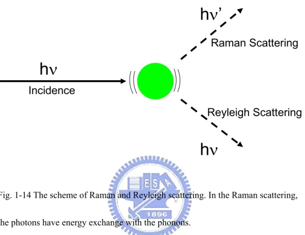
(30) C C 1 EB1 ,C = [Δ1 − Δ 2 + ( D3 − 33 D4 )ε zz ] + ( D1 − 33 D2 )ε zz 2 C13 C13 1 C 1 ±{ [Δ1 − Δ 2 + ( D3 − 33 D4 )ε zz ]2 + 2Δ 22 } 2 4 C13. E(1-26). for the crystal under the biaxial strain. Here, the subscripts correspond to the plus and minus signs in Eq. E(24) and E(16), respectively. C13 and C33 are the elastic constants. Figure 1-13 shows the A, B, and C exciton ground state resonance energies and the first excited resonance energy of A exciton as a functions of εzz. The resonance energies EA, EB, EC, and EA,n=2 increase with εzz increasing. The ground state binding energy of the A-exciton, Eex,A is independent of strain.[76] The least square fit to the data of EA and EA,n=2 yields E A = 3.478 + 15.4ε zz. E(1-27). E A,n = 2 = 3.498 + 15.4ε zz .. E(1-28). The difference between the EA and EA,n=2, Eex,A, is calculated to be 26 meV. The curve of the A-exciton is linear and the slope is 15.4 eV. The nonlinear least-square method yields Δ1, Δ2=Δ3, and D3 −. C33 D4 = 23.6eV . C13. E(1-29). 1.3.3 Strain and Raman Spectrum in GaN Raman scattering spectroscopy is an effective method for studying molecular vibration. Raman scattering was discovered by Raman in 1928. However, before the ‘60s, Raman spectra were very weak because high-power and highly pure light sources were unavailable. Such a source, the laser, was developed in that decade, and was a suitable light source for producing Raman spectra. When incident photons exchange energy with the phonons, Raman scattering 13.
(31) occurs. When the incident photons do not exchange energy with the phonons, Rayleigh scattering occurs. Figure 1-14 presents Raman and Reyleigh scatterings. Raman spectroscopy measures the change of the photons upon scattering with phonons, as follows (where the wavenumber, Δω, is measured in Δcm-1.) Δω =. ΔE hc. E(1.30). When the scattering photons obtain energy from the phonons, Stokes scattering occurs, and is evident in the Raman spectrum: otherwise, the scattering is anti-Stokes scattering. Raman spectra are typically obtained from Stokes scattering because the signal intensity of Stokes scattering exceeds that from anti-Stoke scattering. Phonons in wurtzite structure at the Γ point (k=0) have eight modes 2A1+2E1+2E2+2B1. One of the A1 and one of the E1 modes are acoustic phonon modes. The remaining six phonon modes, A1+E1+2E2+2B1, are optical. Figure 1-15 schematically presents the atomic displacement associated with these optical phonon modes. The B1 modes are silent modes in both Raman and IR spectra because the plus and minus directions of ionic vibration are the same, and so on dipole moment is not generated to interact with the photons. If the atomic displacement is parallel to the G wavevector k , then the optical phonon modes are called longitudinal optical modes G (LO). Otherwise, the atomic displacement is perpendicular to the wavevector k , then. the optical phonon modes are called transverse optical (TO) modes. The Raman spectrum from a wurtzite structure has six active optical phonon modes A1(LO), A1(TO), E1(LO), E1(TO), E2(low) and E2(high). The Raman spectrum is sensitive to the polarization of the incident and scattered photons in a manner that determines the selection rules of the Raman spectral measurement, which, along with familiar values are presented in Tables 1-3 and 1-4.[6-8]. 14.
(32) Phonon transport in crystal is limited by the mean free path of phonons and the stress. The mean free path of phonon vibration in a crystal is called the confinement length, L, which decreases as the density of defects and dislocations, N, increases. L=. 3. 1 N. E(1.31). Reducing L broadens and shifts the Raman phonon frequency signal. Another factor that affects the Raman phonon frequency shift is the strain. However, in most cases of strain analysis by Raman spectroscopy of wurtzite GaN, the effect of L is neglected, because the strain of GaN caused by the hetro-epitaxy is large and the difference between TEC values is large in most cases.[80-83] The residual thermal strain can therefore be estimated using the expression for the Raman spectrum shift, Δωλ = [a1ε zz + a2 (ε xx + ε yy )] + [b1ε zz + b2 (ε xx + ε yy )]. E(1.32). where a1, a2, b1 and b2 are the deformation constants. In the wurtzite structure, the equation E(1.3.30) can be rewritten as Δωλ = [. C33 (2 pλ + qλ r )]σ xx ≡ K λRσ xx (C11 + C12 )C33 − 2C132. where qλ = a1 + b1 , pλ = a2 + b2 , and r =. E(1.33). ε zz −2C13 = . K λR is defined as the ε xx C33. coefficient of σxx. Table 1-5 summarizes of K λR , which is defined as the Raman calibration factor, obtained by various research groups. K λR can be used to calculate the stress of GaN from the Raman phonon frequency shift.. 15.
(33) 1.4 References 1 M. S. Shur, and R. F. Davis, GaN-BASED MATERIALS AND DEVICES: Growth, Fabrication, Characterization and Performance, World Scientific, 33 (2004). 2 S. Nakamura, M. Senoh, N. Iwasa, S. Nagahama, T. Yamada, and T. Mukai, Jpn. J. Appl. Phys. 34, L1332 (1995). 3 C. Y. Yeh, Z. W. Lu, S. Froyen, and Alex Zunger, Phys. Rev. B. 46, 10086 (1992). 4 J. I. Pankove, and T. D. Moustakas, Gallium Nitride (GaN) I: Semiconductors and Semimetals, Acdemic Press (1998). 5. S. Nakamura et al., The Blue Laser Diode: The Complete Story, Springer (2000).. 6. S. Nakamura et al., Introduction to Nitride Semiconductor Blue Lasers and Light Emitting Diodes, Taylor and Francis (2000).. 7 V. W. L. Chin, T. L. Tansley, and T. Osotchan, J. Appl. Phys. 75, 7365(1994). 8 H. Harima, Journal of Physics: Cond. Matter. 14, R967 (2002). 9 S. N. Mohammad, and H. Morcoc, Prog. Quant. El., 20, 361 (1996). 10 Monemar, J. Material Sci.: materials in Electronics, 10, 227 (1999). 11 S. Strite, H. Morcoc, J. Vac. Sci. Technol. B., 10, 1237 (1992). 12 R. Goldhan, S. Shokhovets, in III-nitride semiconductors optical properties II, M. O. Manasreh, H. X. Jiang, editors, Taylor&Francis, 73 (2002). 13 I. Vurgaftman, J.R. Meyer, L.R. Ram-Mohan, J. Appl. Phys., 89, 5815 (2001). 14. V. M Bermudez, C.-I. Wu, A.Khan, J. Appl. Phys., 89, 1991 (2001).. 15 V. YU. Davydov,Yu. E. Kitaev, I. N. Goncharuk, A. N. Smirnov, J. Graul, O. Semchinova, D. Uffmann, M. B. Smirnov, A. P. Mirgorodsky, and R. A. Evarestov, Phys. Rev.B., 58, 12899(1998). 16. W. J. Moore, J. A. Freitas, Jr., S. K. Lee, S. S. Park, and J. Y. Han, Phys. Rev. B.,. 16.
(34) 65, 081201/1 (2002).. 17. M. Wraback, H. Shen, J. C. Carrano, T. Li, J. C. Campbell, M. J. Schurman, and I. T. Ferguson, Appl. Phys. Lett., 76, 1155 (2000).. 18 M. Fanciulli, T. Lei, T. D. Moustakas , Phys. Rev. B., 48, 15144 (1993). 19 R. Stepniewski, A. Wysmolek, K. P. Korona, and J. M. Branowski, in III-nitride semiconductors optical properties I, M. O. Manasreh, H. X. Jiang, editors, Taylor & Francis, 197 (2002). 20 M. Leszczynski, H. Teisseyre, T. Suski, I. Grzegory, M. Bockowski, and J. Jun, Appl. Phys. Lett., 69, 73 (1996). 21 B. Heying, I. Smorchkova, C. Poblenz, C. Elsass, B.Fini, S. Den Baars, U. Mishra, and J.S. Speck, Appl. Phys. Lett., 77, 2885 (2000). 22 D. C. Look, C. E. Stutz, R. J. Molnar, K. Saarinen and Z. Liliental-Weber, Solid State Comm. 117, 571 (2001). 23 S. Nakamura, T. Makui, and M. Senoh, J. Appl. Phys., 71, 5543 (1992). 24 J. G. Kim, A. C. Frenkel, H. Liu and R. M. Park, Appl. Phys. Lett., 65, 91 (1994). 25. D. K. Gaskill, L. B. Rowland, K. Doverspike, (in Properties of Group III Nitrides, Ed. by J. Edgar), EMIS Datareviews series No. 11, 101 (1995).. 26 D. J. As, D. Schikora, A. Greiner, M. Lubbers, J. Mimkes, and K. Lischka, Phys. Rev. B., 54, R11118 (1996). 27. J. R. L. Fernandez, V. A. Chitta, E. Abramof, A. Ferreira da Silva, J. R. Leite, A. Tabata, D. J. As, T. Frey, D. Schikora, and L. Lischka, (in: GaN and Related Alloys - 1999. Symposium (Materials Research Society Symposium Proceedings Vol.595); Warrendale, PA, USA : Mater. Res. Soc. (2000).. 28. J. F. Muth, J. D. Brown, M. A. L. Johnson, Zhonghai Yu, R. M. Kolbas, J. W. Cook, Jr., J. F. Schetzina, MRS Internet J. Nitride Semicond. Res., 4S1, G5.2. 17.
(35) (1999). 29 G. Yu, G. Wang, H. Ishikawa, M. Umeno, T. Soga, T. Egawa, J. Watanabe, and T. Jimbo, Appl. Phys. Lett., 70, 24, 3209 (1997). 30 S. Bloom, G. Harbeke, E. Meier, I. B. Ortenburger, phys. stat. Solidi., 66, 161 (1974). 31 R. Dingle, D. D. Sell, S. E. Stokowski, P. J. Dean and B. Zetterstrom, Phys. Rev. B., 3, 497500 (1971). 32 X. Zhang, Y. T. Hou, Z. C. Feng, and J. L. Chen, J. Appl. Phys., 89, 6165 (2001). 33. O. Ambacher, W. Rieger, P. Ansmann, H. Angerer, T. D. Moustakas and M. Stutzman, Sol. State Comm., 97, 365 (1996).. 34 J. F. Muth, J. H. Lee, I. K. Shmagin, R. M. Kolbas, H. C. Casey, Jr., B. P. Keller, U. K. Mishra, and S. P. DenBaars, Appl. Phys. Lett., 71, 2572 (1997). 35 T. J. Schmidt, J. J. Song, in III-nitride semiconductors optical properties II, M. O. Manasreh, H. X. Jiang, editors, Taylor&Francis, p.3 (2002). 36. R. F. Davis, A. M. Roskowski, E. A. Preble, J. S. Speck, B. Heying, J. A. Freitas, Jr. Glaser, E. R., and W.E. Carlos, Proceedings of the IEEE 90, 993 (2002).. 37. H. X. Jiang, J. Y. Lin, and W. W. Chow, in III-nitride semiconductors optical properties I, M. O. Manasreh, H. X. Jiang, editors, Taylor&Francis, p960 (2002).. 38. B. Monemar, J. P. Bergman, H. Amano, I. Akasaki, T. Detchprohm, K. Hiramatsu, N. Sawaki, Int. Symp. on Blue Laser and Light Emiting diodes, Chiba Univ., Japan, March 5 (1996).. 39 J. Holst, L. Eckey, A. Hoffmann, I. Broser, B. Schottker, D. J. As, D. Schikora and K. Lischka, Appl. Phys. Lett., 72, 1439 (1998). 40. J. Wu, H. Yaguchi, K. Onabe, in III-nitride semiconductors optical properties II, M. O. Manasreh, H. X. Jiang, editors, Taylor&Francis, p.363 (2002).. 18.
(36) 41 J. C. Nipko, C. K. Loong, C. M. Balkas, R. F. Davis, Appl. Phys. Lett., 73, 3435(1998). 42 I. Barin, O. Knacke, and O. Kubaschewski, Thermochemical properties of inorganic substances, Springer-Verlag, Berlin-Heidelberg-New York (1977). 43 D. I. Florescu, V. M. Asnin, F. H. Pollak, R. J Molnar, and C. E. C. Wood, J. App. Phys., 88, 3295 (2000). 44 Kotchetkov, D. J. Zou, A. A. Balandin, D. I. Florescu, and F. H Pollak, Appl. Phys. Lett., 79, 4316 (2001). 45. E. K. Sichel, J. I. Pankove, J. Phys. Chem. Solids., 38, 330 (1977).. 46 J. Zou, D. Kotchetkov, A. A. Balandin, D. I. Florescu, and F. H. Pollak, Journal of Applied Physics., 92, 2534 (2002). 47. A. Polian, M. Grimsditch, and I. Grzegory, J. Appl. Phys., 79, 3343 (1996).. 48. A. F. Wright, J. Appl. Phys., 82, 2833 (1997).. 49 F. Bernardini, V. Fiorentini, Appl. Phys. Lett., 80, 4145 (2002). 50. A. D. Bykhovski, B. L. Gelmont, and M. S. Shur, J. Appl. Phys., 81, 6332 (1997).. 51 I. L. Guy, S. Muensit, E. M. Goldys, Appl. Phys. Lett., 75, 4133 (1999). 52 A. Zoroddu, F. Bernardini, P. Ruggerone, V. Fiorentini, Phys. Rev. B., 64, 045208/1 (2001). 53 M. S. Shur, B. Gelmont and A. Khan, J. Electronic Materials 25, 777 (1996). 54 H. Maruka et. al, Appl. Phys. Lett. 15, 327 (1969). 55. R. J. Molnar et. al, J. Cryst. Growth 178, 147 (1997).. 56. K. Naniwae, S. Itoh, H. Amano, K. Itoh, K. Hiramatsu, and I. Akasaki, J. Cryst. Growth 99, 381 (1990).. 57 S. T. Kim, Y. J. Lee, D. C. Moon, C. H. Hong, T. K. Yoo, J. Cryst. Growth 194,. 19.
(37) 37 (1998). 58. W. Utsumi, H. Saitoh, H. Kaneko, T. Watanuki, K. Aoki and O. Shimomura, Nature Mater. 2, 735 (2003).. 59. T. S. Zheleva, S. A. Smith, D. B. Thomson, T. Gehrke, K. J. Linthicum, P. Rajagopal, E. Carlson, W. M. Ashmawi, and R. F. Davis, MRS Internet J. Nitride Semicond. Res. 4S1, G3.38 (1999).. 60 N. N. Morgan, Y. Zhizhen, X. Yabou, Materials Science and Engineering B90,201 (2002).. 61 B. Beaumont, M. Vaille, G. Natat, A. Bouillé, J. C. Guillaume, P. Vénnègues, S. Haffouz, and P. Gibart, MRS Internet J. Nitride Semicond. Res. 3, 20 (1998). 62 Y. Chen, R. Schneider, S. Wang, R. S. Kern, C. H. Chen, and C. P. Kuo, Appl. Phys. Lett. 75, 2062 (1999). 63. R. Cadoret, et al, J. Cryst. Growth 205, 123 (1999).. 64 E. Aujol, J. Napierala, A. Trassoudaine, E. Gil-Lafon, R. Cadoret, J. Cryst. Growth 222, 538 (2001). 65. R. Cadoret, and A. Trassoudaine, J. Phys. Condens. Matter 13, 6893 (2001).. 66 A. Trassoudaine, R. Cadoret, E. Gil-Lafon, J. Cryst. Growth 260, 7 (2004).. 67 E. Aujol, A. Trassoudaine *, D. Castelluci, R. Cadoret, Mater. Sci. Eng. B 82, 65 (2001).. 68 A. Trassoudaine1, E. Aujol, P. Disseix, D. Castelluci, and R. Cadoret, Phys. Stat. b Sol. (a) 176, 425 (1999). 69 R. Cadoret, A. Trassoudaine1, and E. Aujol, Phys. Stat. Sol. (a) 183, 5 (2001). 70. R. J. Molnar, et al, J. Cryst. Growth 178, 147 (1997).. 71 H. Lee, j. S. Harris, Jr. J. Cryst. Growth 169, 689 (1996). 72. D. K. Schroder, Semiconductor material and Device characterization, 2nd, John. 20.
(38) Wiley & Sons (1998). 73. H. Luth, Surface and Interfaces of Solid materials, 3rd, Springer Verlag, Berlin Heidelberg (1995).. 74. K. N. Tu, J. W. Mayer, L. C. Feldman, Electronic Thin Film Science: For Electrical Engineers & Material Scientists, Macmillan college publishing company (1992).. 75 G. L. Bir, G. E. Pikus, Symmetry and Strain-Induced Effects in Semiconductors, John Wiley & Sons, New York, USA (1974). 76 J. J. Hopfield, J. Phys. Chem. Solids 15, 97 (1960). 77 H. Harima, J. Phys.: Condens. Matter 14, R967 (2002). 78 T. Azuhata, T. Sota, K. Suzuki, and S. Nakarmura, J. Phys.: Condens. Matter. 7, L129 (1995). 79 H. Siegle, L. Eckey, A. Hoffmann, C. Thomsen, B. K. Meyer, D.Schikora, M. Hankeln, and K. Lischka, Solid State Comm. 96, 943 (1995). 80. F. C. Wang, C. L. Cheng, Y. F. Chen, C. F. Huang, and C. C. Yang, Semicond. Sci. Technol. 22, 896 (2007).. 81 J. M. Wagner, F. Bechstedt, Phys. Rev. B 66, 115201 (2002). 82. S. Tripathy, R. K. Soni, H. Asahi, K. Iwata, R. Kuroiwa, K. Asami, S. Gonda, J. Appl. Phys. 85, 8386 (1999).. 83 P. Puech, F. Demangeot, J. Frandon, C. Pinquier, M. Kuball, V. Domnich, Y. Gogotsi, J. Appl. Phys. 96, 2853 (2004). 84 F. Bertram, T. Riemann, J. Christen, A. Kaschner, A. Hoffmann, K. Hiramatsu, T. Shibata, and N. Sawaki, Meterials Science and Engineering B 59, 117 (1999). 85 M. Kuball, M. Benyoucef, B. Beaumont, and P. Gibart, J. Appl. Phys. 90, 3656 (2001).. 21.
(39) 86 T. Kozawa, T. Kachi, H. Kano, H. Nagase, N. Koide, K. Manabe, J. Appl. Phys. 77, 4389 (1995).. 87 C. Kisielowski, J. Kruger, S. Ruvimov, T. Suski, J. W. Ager, E. Jones, Z. L. Weber, M. Rubin, E. R. Weber, M. D. Bremser, R. F. Davis, Phys. Rev. B 54, 17745 (1996). 88. V. Yu. Davydov, N. S. Averkiev, I. N. Goncharuk, D. K. Nelson, I. P. Nikitina, A. S. Polkovnikov, A. N. Smirnov, M. A. Jacobson, and O. K. Semchinova, J. Appl. Phys. 82, 5097 (1997).. 89. F. Demangeot, J. Frandon, P. Baules, F. Natali, F. Semond, J. Massies, Phys. Rev. B 69, 155215 (2004).. 90. S. Nakamura, and S. F. Chichibu, Introduction to Nitride Semiconductor Blue Lasers and Light Emitting Diodes, Taylor & Francis (2000).. 22.
(40) Lighting. Storage. Blue Light LED. White Light LED. UV Light LED. White Light LED. RGB LED. LCD Backlight. Blue LD (InGaN). Blue-Ray Disk High-Definition DVD. Nitride semiconductor. UV LD (AlGaN、AlN). Next DVD. IR LED (InGaN、InN). 1.3、1.5 μm Short Distance. IR LD (InGaN、InN). 1.3、1.5 μm Long Distance. Microwave (GaN、AlGaN). Cellphone、Wireless. High Power (GaN、AlGaN). HEMT. UV LED (GaN、AlGaN). Sterilization、Hygiene. IR LED (GaN、AlGaN). IR Radition、Meducal. InN、InGaN. Solar cell. Communication. High Speed Device. Biochemistry & Medical Energy Save & Environmental Protection. Fig. 1-1 The applications of nitride base optoelectronic devices. 23.
(41) Fig. 1-2 The optimum transform efficiency of different material in visible region. The black real line is the CIE curve for human’s eye.[Lumileds lighting Company]. 24.
(42) Fig. 1-3 The evolution of solid state lighting from 1920, the efficiency of LED increasing several multiples.[ Lumileds lighting Company]. 25.
(43) Fig. 1-4 The relationship of lattice constant and energy gap of different compound semiconductors.. 26.
(44) Ga. c N. a Fig. 1-5 The clinographic projection of the wurtzite structure of GaN. The c and a are the lattice constant.. 27.
(45) Tab. 1-1 The properties of gallium nitride (Shur et al.[1]). Crystal structure. Wurtzite. Zincblende. Group of symmetry. C6V4P63mc. Td2-F43m. Density (g/cm3). 6.15[7,8]. Dielectric constant static. 8.9-9.5[8,9,10,11]. 9.7. high frequency. 5.35[12,8,9,10,11]. 5.3[12]. Lattice constants (A). a = 3.189[13] c = 5.185[14,13]. 4.52[8]-4.50[10,1. Optical phonon energy (meV). 91.8[15,8]. 91.9[8]. 3.5[13]. 3.3[13]. 3]. Band structure Energy gap (eV). Temperature dependence of the energy gap 3.57-7.4×10⁻⁴ ×T2/(T+600) 0<T<600. 3.37-7.4×10⁻⁴ ×T2/(T+600). Conduction band Effective electron mass (in units of mo). 0.22[16,13,17]. Effective conduction band density of states 2.6×10¹⁸ (cm-3) Ionization energies of shallow donors Si (eV). 0.012-0.03. O (eV). 0.004-0.01. 0.15[18] 1.4×10¹⁸. Valence band Energy of spin-orbital splitting ESO(eV). 0.011-0.018[19,13]. Energy of crystal-field splitting Ecr (eV). 0.011-0.022[19,13]. 0.017[13]. Effective hole mass (in units of mo) heavy. 1.0[13]. 28. 1.3[18,20].
(46) Effective valence band density of states (cm-3). 2.5×10¹⁹. 4.1×10¹⁹. Ionization energies of shallow acceptors. Mg (eV). 0.14-0.21. Zn (eV). 0.21. Native defect VGa (eV). 0.14. Electrical properties Breakdown field (Vcm-1). ~5×10⁶ [8]. ~5×10⁶. Mobility (cm2 V-1s-1) Electrons. ~1000[21,22,8223]. ≤1000[24]. ≤ 200[25]. ≤ 350[26,27]. Electrons. 25. 25. holes. 5. 9. Holes Diffusion coefficient(cm2s-1). Optical properties Infrared refractive index. 2.3[8]. Refractive index spectra. [28,29]. Reflectance spectra. [30,31,19,32]. Absorption spectra. [33,31,12,28,34,35]. Photoluminescence spectra. [36, 37,38, 19,35] 820[41]. Specific heat at 300K (Jg-1°C-1) 298<T<1773 (see also [83]). 0.49[41] 0.456+0.107×10⁻³T[42]. Thermal conductivity (Wcm-1°C-1). >1.95 [43,44,45,46]. Thermal diffusivity (cm2s-1). 0.65. Thermal expansion, linear ( °C-1 ). αa = 5.59×10⁻⁶ [8] αc = 3.17×10⁻⁶ [8]. 29. [12]. [39,40].
(47) Mechanical properties Elastic constants (GPa) C11. 390±15[47]. 293[48]. C12. 145±20[47]. 159[48]. C13. 106±20[47]. C33. 398±20[47]. C44. 105±10[47]. 155[48]. Piezoelectric constants (cm-2) [49,50,51,13,52]. e15. −0.30. e31. (−0.3)−(−0.55). e33. 0.6−1.12 1.27. e14. 0.4[53]. 30.
(48) Fig. 1-6 The phase diagram of GaN.[58]. 31.
(49) APC. Oven Reactor. E-Rack. Ball Valve. Particle trap MFC. MFC. EPC. MFC. MFC. MFC. Throttle valve. PUMP NH3. SiH4. H2. HCl. N2. Fig. 1-7 The sketch of HVPE system.. 32. H2. Exhaust.
(50) 1. 2. 6. 3. 7. 4. 5. 8. 9. Fig. 1-8 The reactor of HVPE system. Including: 1. Oven 2. Quartz tube 3. HCl line 4. Gallium boat 5. Shower head 6. NH3 line 7. Ambient gases line 8. Mixing box 9. Susceptor 10. Wafer holder. 33. 10.
(51) Tab. 1-2 The methods of bulk GaN growth (IWN 2006). Methods of Bulk GaN Growth Na flux. Ammonothermal. N2 high pressure. HVPE. (LPE) Temperature. 500~800 oC. 400~600 oC. 1400~1550 oC. 1000 oC. Pressure. 50~100 atm. < 1500 atm. 15000 atm. ~ 1 atm. Size. 45 mm. 1”. Several mm. > 2”. Character. No bulk porduct. The same technique as. The setup is large an. Sunstrate. hydro-thermal method. expensive. Complexity (expensive). with mass production results Organization. Tohoku Univ.. Tohoku Univ.. Unipress (Poland). Sumitomo. Cornell Univ.. Naval research (USA). Japan energy. Hitachi Cable. Osaka Univ.. Air Force (USA). Yamaguchi Univ.. Mitsubishi Chemical. NGK. UCSB (USA). Lumilog. Ammon (Poland). ITRI. Nichia (with Ammon). Chiao-Tung Univ.. Mass production reference. No! JJAP 45, L1136. J. Cryst. Growth 260, 67. J. Cryst. Growth 274, 55. (2006). (2004). (2005). 34. OK!.
(52) Ga N H Cl. (a). V. N Ga. (b). NH3. 35.
(53) (c). H Cl Ga N. (d). HCl. Ga N. 36.
(54) (e). GaCl3. Fig. 1-9 The growth model in vapor phase epitaxy of GaN.. 37.
(55) Fig. 1-10 Equilibrium partial pressures of gaseous species inside the reactor.[71]. 38.
(56) Stress=0 Tensile Stress. d. Compressive Stress. z ½ tf. Substrate r. Fig. 1-11 The Stress distribution in thick-film with substrate. The r denotes the curvature radius of bowing film.. 39.
(57) Zincblende. Conduction Band. Γ6. Wurtzite. Γ1. Γ1. Γ7. ┴ // Γ8 Valence Band. Δ Γ7 so. Γ9. Γ5. Γ5. A B C ┴ ┴ // (//) (┴). Δso Δcr. Γ7. Γ1 Crystal Field. Spin-Orbit. Fig. 1-12 The Band structures and respective transition in GaN. The indications ┴ and // show the transition is allowed for the polarization perpendicular and parallel to the optic axis, respectively. The value Δso and Δcr are the spin-orbit and crystal-field splittings, respectively.[80]. 40. Γ7.
(58) Fig. 1-13 Strain dependence of the free exciton resonance energies in wurtzite GaN. εzz=(c-c0)/c0 denotes the strain along the z-axis.[80]. 41.
(59) hν’ Raman Scattering. hν Incidence Reyleigh Scattering. hν Fig. 1-14 The scheme of Raman and Reyleigh scattering. In the Raman scattering, the photons have energy exchange with the phonons.. 42.
(60) N. Ga. E1. E2 (low). E2 (high). N. Ga. A1. B2 (low). Fig. 1-15 Optical phonon modes in wurtzite structure crystal.. 43. B1 (high).
(61) Tab. 1-3 Raman selection rule for optical phonon in wurtzite structure (x//a) Scattering Configurations. Allowed Modes. y ( x, x ) y. A1(TO)、E2(high)、E2(low). y ( z, z ) y. A1(TO). y ( z , x) y. E1(TO). z ( x, x ) z. A1(TO)、E2(high)、E2(low). z ( x, y ) z. E2(high)、E2(low). z ( y, y ) z. A1(LO) 、E2(high)、E2(low). z( y , y ) z. A1(TO) 、E2(high)、E2(low). z( y , x ) z. E1(TO)、E1(LO). 44.
(62) Tab. 1-4 Familiar Raman phonon frequency values in wurtzite structure of GaN E1(low). A1(TO). E1(TO). E2(high). A1(TO). E1(LO). 144. 531.8. 558.8. 567.6. 734. 741. [77]. 144. 533. 561. 569. 735. 743. [78]. 533. 561. 570. 735. 742. [79]. 45.
(63) Tab. 1-5 Raman calibration factor. Group. Growth. [GPa-1cm-1]. Method T. Kozawa et al.. KλR. Substrate. MOCVD. sapphire. 6.2. HVPE. sapphire. 4.24. MOCVD. 6H-SiC. 2.7. MBE. sapphire. 4.86. MOCVD. sapphire. 2.9. MBE. Si(111). 2.43. MOCVD. sapphire. 2.56. (1995)[86] C. Kisielowski et al. (1996) [85, 87] V. Yu. Davydov et al. (1997)[88] S. Tripathy et al. (1999)[82] M. Kuball et al. (2001)[85] F. Demangeot et al. (2004)[91] F. C. Wang et al. (2007)[80]. 46.
(64) Chapter 2. Air-bridged Epitaxial Lateral Overgrowth The epitaxial lateral overgrowth (ELOG) technology was applied to produce high quality GaN with at least one order of magnitude reducing of threading dislocation density. Numerous modifications of ELOG process have been proposed in order to improve it, such as pendeo ELOG, facet controlled ELOG, air-bridged ELOG, and patterned substrate ELOG. For relaxing the thermal stress and developing self-separation technology of bulk GaN, two kind of trenched ELOG structures were investigated in this chapter, called high-void air-bridged ELOG and dot air-bridged ELOG. These structures can reduce the thermal stress and dislocation density of bulk GaN, indeed, self-separated it from sapphire substrate.. 2.1 High-Void Air-Bridged Technique. 2.1.1 Introduction of Air-Bridged technique Most current nitride-based devices are hetero-epitaxially grown on lattice-mismatched substrates, such as sapphire, Si, GaAs, and SiC. The large mismatches between the lattice constants of substrates and epitaxial films generate. 47.
(65) high dislocation densities. Furthermore, differences between the thermal expansion coefficients (TEC) of the substrates and the epitaxial films as shown in Tab. 2-1 cause large warp or bowing of the epi-layers. Selective epitaxial techniques, such as lateral epitaxial overgrowth (LEO) and pendeo epitaxy (PE) have been demonstrated to be extremely effective in reducing threading dislocations (TDs) density by over two orders of magnitude in two to several steps of laterally grown GaN films on sapphire and SiC substrates.[1-4] However, c-axis tilting in the wing region, of commonly 0.2o-1o, are normally observed in both LEO and pendeo structures in an azimuth perpendicular to the LEO or PE stripe direction. When wing tilt is present, the coalescence of nearby stripes may yield arrays of dislocations, reducing the defect-free region of overgrown GaN.[5] Kidoguchi et al., proposed a new method of lateral growth called air-bridged LEO to improve the wing tilting of conventional selective epitaxy.[6-8] The dry etching and standard photolithography technique were employed to produce trenches in a GaN template, and the sidewall of GaN trenches was covered with a dielectric mask such as SiNx or SiO2 in air-bridged LEO structure. After the regrowth of GaN, the voids of the air-bridged structure were buried in the coalesced GaN wings. Currently, however, the effect of the voids height in an air-bridged structure is still not clearly understood, especially in the stress distribution caused by the difference between the TECs of the epitaxial films and the substrate in. 48.
(66) thick GaN films.. 2.1.2 Experiment In this investigation, a specially designed air-bridged structure with high voids was developed to grow thick GaN layers using HVPE. The quality of the GaN layers grown by this technique was compared to that of GaN layers that were prepared by a more conventional pendeo growth process with lower voids. The HVAB structure with the higher voids is proposed to reduce the density of TDs, the residual stress induced by the difference between TECs, and to obtain the self-separated freestanding GaN wafer from the sapphire substrate.[9] To provide a meaningful comparison, a 4 μm-thick GaN layer was initially grown on a c-plane sapphire substrate by metal-organic chemical vapor deposition (MOCVD). Then, a standard photolithographic technique was applied to fabricate a pattern of 4 μm-wide GaN seed stripes and 6 μm-wide grooves between adjacent stripes in the < 1 100 > direction of GaN. Dry etching was employed to form the trenches with 0.2 μm-deep etched into the sapphire. The GaN template was then sliced into two half-wafers. One of the half-wafers (pendeo structure) remained without any additional treatment. The other half-wafer (HVAB structure) was passivated with a thin oxide layer on the sidewall of the GaN seed. The two. 49.
數據
![Fig. 1-3 The evolution of solid state lighting from 1920, the efficiency of LED increasing several multiples.[ Lumileds lighting Company]](https://thumb-ap.123doks.com/thumbv2/9libinfo/8121843.165923/42.892.177.740.196.564/evolution-lighting-efficiency-increasing-multiples-lumileds-lighting-company.webp)

+7
![Fig. 1-10 Equilibrium partial pressures of gaseous species inside the reactor.[71]](https://thumb-ap.123doks.com/thumbv2/9libinfo/8121843.165923/55.892.161.670.182.723/fig-equilibrium-partial-pressures-gaseous-species-inside-reactor.webp)
![Fig. 1-13 Strain dependence of the free exciton resonance energies in wurtzite GaN. ε zz =(c-c 0 )/c 0 denotes the strain along the z-axis.[80]](https://thumb-ap.123doks.com/thumbv2/9libinfo/8121843.165923/58.892.271.570.210.681/strain-dependence-exciton-resonance-energies-wurtzite-denotes-strain.webp)
相關文件
Yu-Chun
Program C: Differential Geometry and Geometric Analysis Nan Kuo Ho (NTHU)—Program Chair. River Chiang (NCKU) Chun-Chi Lin (NTNU) Chung-Jun
B3-4 DEEP LEARNING MODEL COMPRESSION BY NETWORK SLIMMING Ching-Hao Wang (王敬豪), Shih-Che Chien (簡士哲), Feng-Chia Chang (張峰嘉), and Wen-Huang Cheng (鄭文皇). B3-5
--coexistence between d+i d singlet and p+ip-wave triplet superconductivity --coexistence between helical and choral Majorana
Nicolas Standaert, "Methodology in View of Contact Between Cultures: The China Case in the 17th Century ", Centre for the Study of Religion and Chinese Society Chung
Natural Terrain Landslide Risk Mitigation Measures at Yu Tung Road, Tung Chung.. Natural Terrain Landslide Risk Mitigation Measures at Yu Tung Road,
Shang-Yu Su, Chao-Wei Huang, and Yun-Nung Chen, “Dual Supervised Learning for Natural Language Understanding and Generation,” in Proceedings of The 57th Annual Meeting of
• Zhen Yang, Wei Chen, Feng Wang, Bo Xu, „Improving Neural Machine Translation with Conditional Sequence Generative Adversarial Nets“, arXiv 2017. • Supervised
