Temperature dependent gain characteristics in
GaN-based vertical-cavity surface-emitting
lasers
Tien-Chang Lu,1,2* Bo-Siao Cheng,1 and Mei-Chun Liu1
1
Department of Photonics, National Chiao-Tung University, 1001 Ta Hsueh Rd., Hsinchu 300, Taiwan
2
Institute of Lighting and Energy Photonics, National Chiao-Tung University, 301, Gaofa 3rd Rd., Guiren Township, Tainan County 711, Taiwan
Abstract: Temperature dependent gain characteristics and linewidth
enhancement factor (α-factor) of vertical-cavity surface-emitting lasers with InGaN/GaN multiple quantum wells were studied by measuring the photoluminescence spectra below the threshold condition and analyzed by using the Hakki-Paoli method. The optical gain and differential gain showed a more rapid increase as a function of the injected carriers as temperature decreased. The α-factor for the lasing mode was estimated as 2.8 at room temperature and decreased to a value as low as 0.6 at 80 K.
©2009 Optical Society of America
OCIS codes: (140.2020) diode laser; (250.7270) vertical emitting lasers References and links
1. T. Someya, R. Werner, A. Forchel, M. Catalano, R. Cingolani, and Y. Arakawa, “Room temperature lasing at blue wavelengths in gallium nitride microcavities,” Science 285(5435), 1905–1906 (1999).
2. Y. K. Song, H. Zhou, M. Diagne, A. V. Nurmikko, R. P. Schneider, Jr., C. P. Cuo, M. R. Krames, R. S. Kern, C. Carter-Coman, and F. A. Kish, “A quasicontinuous wave, optically pumped violet vertical cavity surface emitting laser,” Appl. Phys. Lett. 76(13), 1662 (2000).
3. C. C. Kao, Y. C. Peng, H. H. Yao, J. Y. Tsai, Y. H. Chang, J. T. Chu, H. W. Huang, T. T. Kao, T. C. Lu, H. C. Kuo, S. C. Wang, and C. F. Lin, “Fabrication and performance of blue GaN-based vertical-cavity surface
emitting laser employing AlN/GaN and Ta2O5/SiO2 distributed Bragg reflector,” Appl. Phys. Lett. 87(8), 081105
(2005).
4. T. C. Lu, C. C. Kao, H. C. Kuo, G. S. Huang, and S. C. Wang, “CW lasing of current injection blue GaN-based vertical cavity surface emitting laser,” Appl. Phys. Lett. 92(14), 141102 (2008).
5. Y. Higuchi, K. Omae, H. Matsumura, and T. Mukai, “Room-Temperature CW Lasing of a GaN-Based Vertical-Cavity Surface-Emitting Laser by Current Injection,” Appl. Phys. Lett. 1, 121102 (2008).
6. C. H. Henry, “Theory of the linewidth of semiconductor lasers,” IEEE J. Quantum Electron. 18(2), 259–264 (1982).
7. B. W. Hakki, and T. L. Paoli, “cw degradation at 300°K of GaAs double-heterostructure junction lasers. II. Electronic gain,” J. Appl. Phys. 44(9), 4113 (1973).
8. J. T. Chu, T. C. Lu, M. You, B. J. Su, C. C. Kao, H. C. Kuo, and S. C. Wang, “Emission characteristics of optically pumped GaN-based vertical-cavity surface-emitting lasers,” Appl. Phys. Lett. 89(12), 121112 (2006). 9. U. T. Schwarz, E. Sturm, W. Wegscheider, V. Kümmler, A. Lell, and V. Härle, E. Sturm, W. Wegscheider, V.
Kummler, A. Lell, and V. Harle, “Optical gain, carrier-induced phase shift, and linewidth enhancement factor in InGaN quantum well lasers,” Appl. Phys. Lett. 83(20), 4095 (2003).
10. A. V. Sakharov, W. V. Lundin, I. L. Krestnikov, V. A. Semenov, A. S. Usikov, A. F. Tsatsul’nikov, Yu. G. Musikhin, M. V. Baidakova, Zh. I. Alferov, N. N. Ledentsov, A. Hoffmann, and D. Bimberg, “Surface-mode lasing from stacked InGaN insertions in a GaN matrix,” Appl. Phys. Lett. 74(26), 3921 (1999).
11. M. O. Manasreh, “Optical absorption near the band edge in GaN grown by metalorganic chemical-vapor deposition,” Phys. Rev. B 53(24), 16425–16428 (1996).
12. I. D. Henning, and J. V. Collins, “Measurements of the semiconductor laser linewidth broadening factor,” Electron. Lett. 19(22), 927 (1983).
13. H. D. Summers, P. Dowd, I. H. White, and M. R. T. Tan, “Calculation of differential gain and linewidth enhancement factorin 980-nm InGaAs vertical cavity surface-emitting lasers,” IEEE Photon. Technol. Lett. 7(7), 736–738 (1995).
14. K. G. Gan, and J. E. Bowers, “Measurement of gain, group index, group velocity dispersion, and linewidth enhancement factor of an InGaN multiple quantum-well laser diode,” IEEE Photon. Technol. Lett. 16(5), 1256– 1258 (2004).
1. Introduction
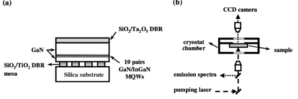
GaN-based blue/violet vertical cavity surface-emitting lasers (VCSELs) have attracted much attention due to many advantageous properties over edge emitting lasers, including circular beam shapes, light emission in the vertical direction, and two-dimensional arrays on the wafer level. Efforts to obtain optically pumped stimulated emission in GaN-based VCSELs have been reported by several groups [1–3]. Recently, the 77K and room temperature electrically pumped GaN-based VCSELs have been reported [4,5]. However, the gain characteristics of VCSELs with InGaN nultiple quantum wells (MQWs) have not been well studied. Gain characteristic is an important parameter of semiconductor lasers since it will influence on threshold, and laser output power. In addition, the linewidth enhancement factor (α-factor) characterizes the performances of semiconductor lasers, such as spectral linewidth broadening under CW operation and wavelength chirping under the high-frequency modulation [6], which is also a key parameter for the laser operation. In this study, the temperature dependent gain and α-factor of the GaN-based VCSEL were characterized. The GaN-based VCSEL with two dielectric distributed Bragg mirrors (DBRs) and an InGaN/GaN MQWs active layer was fabricated using the laser lift-off (LLO) technique. Unlike the conventional short cavity with only few wavelength thickness, the distinct feature of this structure is that the effective cavity length is about 4.2 µm and several cavity modes with about 7 nm mode spacing can be observed from the photoluminescence measurement. As a result, the optical gain spectra and linewidth enhancement factors can be simultaneously analyzed by using the Hakki-Paoli method [7], which was commonly used in analyzing the edge emitting lasers with multiple longitudinal modes. Although the longitudinal modes in our VCSEL structures are not as many as those in the edge emitting lasers, the overall gain spectra can still be clearly observed. pumping laser emission spectra CCD camera (b) cryostat chamber sample Silica substrate 10 pairs GaN/InGaN MQWs SiO2/TiO2DBR mesa SiO2/Ta2O5DBR GaN (a) pumping laser emission spectra CCD camera (b) cryostat chamber sample Silica substrate 10 pairs GaN/InGaN MQWs SiO2/TiO2DBR mesa SiO2/Ta2O5DBR GaN (a)
Fig. 1. (a) Schematic structure of the GaN-based VCSEL sample. (b) Experiment setup.
2. Experiment
The VCSEL layer structure grown on a (0001)-oriented sapphire substrate by metal organic chemical vapor deposition included: a 30-nm GaN nucleation layer, a 4-µm n-type GaN bulk
layer, MQWs consisting of ten periods of 5-nm GaN barriers and 2.5-nm In0.1Ga0.9N wells,
and a 200-nm p-type GaN cap layer. A six-pair DBR of SiO2 and TiO2 was evaporated on the
top of the grown VCSEL structure to form the first dielectric mirror. The sample was then subjected to a laser lift-off (LLO) process using a KrF excimer laser to remove the sapphire substrate. The final thickness of the epitaxial structure after LLO and polishing process was about 4 µm. The detailed process procedure was described elsewhere [8]. The second
dielectric DBR consisting of eight pairs of SiO2 and Ta2O5 was then deposited on the n-type
GaN surface to form the GaN-based VCSELs structure as depicted in Fig. 1(a). Next, an array of circular mesas with diameters of 60 µm was formed by standard lithography and chemical wet etching process through the second dielectric DBR.
The fabricated GaN-based VCSELs were optically pumped by a Nd:YVO4 laser at 355
nm, with a repetition rate of 1 KHz and a pulse width of 0.5 ns. As shown in Fig. 1(b), the pumping laser beam with a spot size of about 40 µm in diameter was vertically incident on the
VCSEL sample from the SiO2/Ta2O5 DBR mesa. The light emission from the VCSEL sample
was collected by an imaging optic into a spectrometer with a spectral resolution of 0.1 nm.
The emission patterns were detected by a CCD camera from the SiO2/TiO5 DBR side through
the mesa aperture. The temperature dependent characteristics were measured under 80K, 150K, 220K and 300K using a temperature-controlled cryogenic chamber.
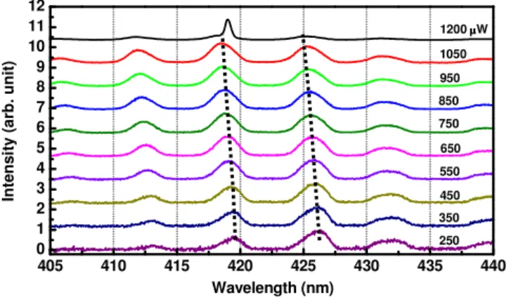
405 410 415 420 425 430 435 440 0 1 2 3 4 5 6 7 8 9 10 11 12 950 250 350 450 550 650 750 850 1050 1200 µµµµW In te n s it y ( a rb . u n it ) Wavelength (nm)
Fig. 2. The PL spectral evolution of the VCSEL under different pumping power levels at 300K. The PL intensity is normalized for comparisons.
3. Results and discussion
Figure 2 shows the normalized photoluminescence (PL) spectra of the GaN-based VCSEL under different pumping power levels at 300K. The PL spectra indicate that there are about six axial cavity modes with a mode spacing about 7 nm, corresponding to a cavity length of 4.2 µm, which is nearly equal to the thickness of the epitaxial cavity. Above the threshold condition, only one lasing mode at 419 nm dominates. The optical gain can be therefore estimated using the Hakki-Paoli method to analyze these multiple cavity modes from the photoluminescence spectra below the threshold condition. By applying the Hakki-Paoli method [7], the material gain in a VCSEL structure can be expressed as:
(
)
1 1 2 2 1 2 1 1 2 2 1 ( ) ( ) 1 ( ) ln ln . 2 ( ) ( ) i I I G R R L L I I α λ + − + − − = − + Γ + Γ Γ (1)where λ is the wavelength at which the cavity modes are being measured. Confinement factor
of the laser structure is estimated as Γ = 0.7% by calculating the spatial overlap between the
optical field and MQWs layers in the VCSEL cavity. Since the range of 10 InGaN/GaN quantum wells spans over a half-wavelength thickness in the cavity, the confinement factors
for different longitudinal mode numbers could be treated as the same. I+ and I− are the
maximum and minimum PL intensities for each cavity mode obtained from the measured PL
spectra, R1 and R2 are DBRs reflectivities which are 99% and 98%, respectively. αι is the
average internal loss of the cavity, which is dominated by the absorption of thick GaN n-type
and p-type layers and was set to be 30 cm−1 [9]. L is the effective cavity length of 4.2 µm.
Under different pumping levels, the I+ and I− would vary and the individual gain for each
cavity modes can be obtained from the Eq. (1). The gain spectra of the VCSEL under different pumping power levels at 300K are shown in Fig. 3(a). Each data point was calculated from the corresponding cavity mode in Fig. 2. The gain curves show an increasing trend as the
pumping intensity increases and the gain bandwidth keeps broadening. In addition, the mode peaks blue shift shown as dashed lines in Fig. 2 due to the increase of the optical gain. At
room temperature, the peak material gain of 2.9 × 103 cm−1 for InGaN/GaN MQWs was
obtained at the threshold condition. The gain spectra under different temperature at 220K, 150K and 80K were also obtained with the same measurement and calculation method and shown in Figs. 3(b), 3(c) and 3(d), respectively.
@300 K @220 K 400 410 420 430 440 450 -12 -10 -8 -6 -4 -2 0 2 4 Wavelength (nm) µµµµW 950 850 750 650 550 450 350 G ain ( x10 3 cm -1) L o ss ( x10 3 c m -1 ) 400 410 420 430 440 450 -12 -10 -8 -6 -4 -2 0 2 4 Wavelength (nm) µµµµW 950 850 730 650 560 450 350 250 G a in ( x 1 0 3 c m -1) L o s s ( x 1 0 3 c m -1 ) 400 410 420 430 440 450 -12 -10 -8 -6 -4 -2 0 2 4 Wavelength (nm) µµµµW 520 450 400 350 300 250 250 150 G a in ( x 1 0 3 c m -1 ) L o s s ( x 1 0 3 c m -1 ) @150 K 400 410 420 430 440 450 -12 -10 -8 -6 -4 -2 0 2 4 G a in ( x 1 0 3 c m -1) L o s s ( x 1 0 3 c m -1 ) Wavelength (nm) µµµµW 300 250 200 105 100 @80 K
(b)
(a)
(c)
(d)
@300 K @220 K 400 410 420 430 440 450 -12 -10 -8 -6 -4 -2 0 2 4 Wavelength (nm) µµµµW 950 850 750 650 550 450 350 G a in ( x 1 0 3 c m -1) L o s s ( x 1 0 3 c m -1 ) 400 410 420 430 440 450 -12 -10 -8 -6 -4 -2 0 2 4 Wavelength (nm) µµµµW 950 850 730 650 560 450 350 250 G a in ( x 1 0 3 c m -1) L o s s ( x 1 0 3 c m -1 ) 400 410 420 430 440 450 -12 -10 -8 -6 -4 -2 0 2 4 Wavelength (nm) µµµµW 520 450 400 350 300 250 250 150 G a in ( x 1 0 3 c m -1 ) L o s s ( x 1 0 3 c m -1 ) @150 K 400 410 420 430 440 450 -12 -10 -8 -6 -4 -2 0 2 4 G a in ( x 1 0 3 c m -1) L o s s ( x 1 0 3 c m -1 ) Wavelength (nm) µµµµW 300 250 200 105 100 @80 K(b)
(a)
(c)
(d)
Fig. 3. The gain spectra of the VCSEL under different pumping level at (a) 300K, (b) 220K, (c) 150K, and (d) 80K.
The pumping power dependence of the peak gain of the lasing mode (at ~420 nm) is plotted as dotted points in Fig. 4(a) for different measurement temperature. The figure shows that the pumping power or injected carrier density required to reach a given gain increases with increasing temperature. These dotted points for different measurement temperature in Fig. 4(a) can be further fitted as the solid curves by the logarithmic law to express the relation
between gain and pumping power in QWs as g(P) = g0ln(P/P0), where g0 is a constant
describing the increasing rate of gain corresponding to the increasing pumping power. The
increase of g0 with a decreasing temperature is shown in Fig. 4(b). It implies that the gain
increase more rapidly as a function of the pumping power or injected carrier density at lower temperature, which could be resulted from several reasons. Firstly, the ratio of radiative to nonradiative recombination is higher at low temperature than that at high temperature. Secondly, carrier overflow becomes pronounced at higher temperatures resulting in less radiative recombination in the MQWs and consequently a lower gain [10]. Another main cause is the broadening of Fermi occupation probability function which spreads carriers over a larger energy range for a given overall carrier density. The result is a lower spectral concentration of inverted carriers, which leads to a broadening and flattening of the gain spectrum. The carrier density in MQWs could be further estimated from the power density of the pumping laser assuming that the pumping light with the emission wavelength of 355 nm
98% absorption in the thick GaN layer with a absorption coefficient at room temperature of
about 104 cm−1 [11]. At room temperature, the threshold carrier density was estimated to be
about 6.5 × 1019 cm−3. 50 100 150 200 250 300 6.0x10² 8.0x10² 1.0x10³ 1.2x10³ 1.4x10³ 1.6x10³ g0 ( c m -1) Temperature (o K) (b) (a) 0 100 200 300 400 500 600 700 800 900 1000 1.0x10³ 1.5x10³ 2.0x10³ 2.5x10³ 3.0x10³ P e a k g a in ( c m -1)
Pumping power (uW)
80K 150K 220K 300K 50 100 150 200 250 300 6.0x10² 8.0x10² 1.0x10³ 1.2x10³ 1.4x10³ 1.6x10³ g0 ( c m -1) Temperature (o K) (b) (a) 0 100 200 300 400 500 600 700 800 900 1000 1.0x10³ 1.5x10³ 2.0x10³ 2.5x10³ 3.0x10³ P e a k g a in ( c m -1)
Pumping power (uW)
80K 150K 220K 300K
Fig. 4. (a) The pumping power dependence of the material peak gain was depicted as dotted points for different temperature. The solid curves were fitted to the measured data for different
temperature respectively. (b) The g0 factor as a function of temperature.
The linewidth enhancement factor can be measured from the amplified spontaneous
emission spectra below the threshold condition [12]. The α-factor is the ratio of the change of
the refractive index (n) with carrier density (N) respect to the change in optical gain with
carrier density and can be expressed by
2 d L dg π λ α λ = ∆ (2)
where λ is the wavelength of each mode peak, ∆λ is the cavity mode spacing, L is the cavity
length, dλ is the wavelength shift when the carrier density is varied by dN, and dg is the
change in optical gain as the carrier is changed by dN. The term of carrier density change is
eliminated in Eq. (2), the α-factor can be directly calculated from the wavelength shift in the
gain spectra under different pumping power levels below the threshold. Since the pumping laser operated at the pulsed mode, the peak shift of longitudinal modes in the cavity due to the temperature rise under pumping could be neglected.
The calculated α-factors as a function of wavelength for different measurement
temperature are shown in Fig. 5. The α-factor shows dependence on wavelength and is smaller
at shorter wavelength. As temperature varied, taking the lasing mode for example, the α
-factors decrease with the decreasing temperature. However, the increase or decrease of α
-factor with respect to the temperature could be due to two different mechanisms in VCSEL operations. As the temperature increased, the lasing wavelength is detuned to the shorter
wavelength side of the gain peak, thus the α is reduced as the laser operates closer to the
differential gain maximum, whereas the lasing operation away from the gain maximum could
increase the carrier density required to the threshold condition, and thus increase the α value
[13]. In our case, the decrease of α values as the temperature goes down could be mainly due
to the reduction of carrier density in the QWs. For the lasing mode, the α-factors varied from
2.8 to 0.6 as the temperature varied from 300K to 80K. In comparison to the InGaN/GaN edge
emitting laser structure that the α value varies between 2.5 and 10 [14], the linewidth
400 405 410 415 420 425 430 435 0.0 0.5 1.0 1.5 2.0 2.5 3.0 3.5 4.0 Lasing mode L in e w id th e n h a n c e m e n t fa c to r Wavelength (nm) 300K 220K 150K 80K
Fig. 5. The α-factor as a function of wavelength obtained at different temperature. The α-factor is smaller at shorter wavelength and decreases as decreasing temperature.
4. Conclusion
In summary, we applied the Hakki-Paoli method to analyze the temperature dependent optical gain and linewidth enhancement factor of VCSELs with InGaN/GaN MQWs. Due to multiple cavity modes in the structure, the optical gain can be obtained by measuring the photoluminescence spectra below the threshold condition. Under different ambient temperature, it is found that the gain increases more rapidly as a function of the pumping
power at lower temperature. The α-factor shows dependence on the wavelength and was
smaller at shorter wavelength. The α-factor at room temperature was estimated as 2.8 and
decreased to as low as 0.6 at 80K. The characterization of temperature dependent gain and α
-factor provides further understanding in operation of the GaN-based VCSEL.
Acknowledgements
The authors would like to gratefully acknowledge Prof. S. C. Wang, and H. C. Kuo at National Chiao Tung University for their fruitful suggestions. This work was supported by the MOE ATU program and in part by the National Science Council of Republic of China (ROC) in Taiwan under contract No. NSC-96-2120-M-009-006 and NSC-96-2221-E-009-067.