Recent Progress on GaN-based Vertical Cavity Surface Emitting
Lasers
T. C. Lu*, C. C. Kao, G. S. Huang, H. C. Kuo and S. C. Wang
Department of Photonics & Institute of Electro-Optical Engineering,
National Chiao Tung University
Ta Hsueh Rd. Hsinchu, 30050, Taiwan
*Correspondence: Phone: 886-3-5131234; Fax: 886-3-5716631; E-mail: [email protected]
ABSTRACT
We report the recent progress of GaN-based VCSELs with two different laser structures. One is a hybrid cavity structure comprised an epitaxial AlN/GaN DBR, an InGaN/GaN MQW active region and a top dielectric DBR. Another is a dielectric cavity structure comprised an InGaN/GaN MQW layer sandwiched by two dielectric DBRs. Both lasers achieved laser action under optical pumping at the room temperature with narrow linewidth. The detailed characteristics of VCSELs will be reported. The status of the electrically pumped VCSEL will also be presented.
Keywords: GaN, VCSELs, DBRs
1. INTRODUCTION
GaN-based optoelectronic devices such as light emitting devices and lasers have become important devices for practical applications such as display, storage, and illumination. Vertical cavity surface emitting laser (VCSEL) structure, in particular can emit a single longitudinal mode with a symmetrically circular beam and a small beam divergence that are superior than the edge emitting lasers and desirable for many practical applications in high density optical storage, laser printing, etc. In the GaN-based VCSEL structure, a micro cavity with a few λ in the optical thickness and a pair of high reflectivity (above 99%) distributed Bragg reflectors (DBRs) are necessary for reducing the lasing threshold. The requirement of high reflectivity and high quality DBRs using AlxGa1-xN and GaN materials is quite challenging since these two materials have large lattice mismatch and difference in thermal expansion coefficients that tends to form cracks in the epitaxially grown DBR structure. These cracks in DBR could result in the reduction of reflectivity and increase in scattering loss. Recently, several groups have reported optically pumped GaN-based VCSELs mainly using three different kinds of vertical resonant cavity structure forms: (1) monolithic grown vertical resonant cavity consisting of epitaxially grown III-nitride top and bottom DBRs (all epitaxial DBR VCSEL), (2) vertical resonant cavity consisting of dielectric top and bottom DBR (dielectric DBR VCSEL), and (3) vertical resonant cavity consists of an epitaxially grown III-nitride top DBR and a dielectric DBR (hybrid DBR VCSEL) [1-4] .
In this paper, we first describe the fabrication technology of GaN-based VCSELs with two types of VCSELs with different microcavity structures for optical pumping. First type has a hybrid microcavity structure that consists of an epitaxially grown AlN/GaN DBR, a GaN active layer with InGaN/GaN MQWs, and a Ta2O5/SiO2 dielectric DBR. Second type has a dielectric DBR microcavity structure that has a similar InGaN/GaN MQWs active layer sandwiched in two dielectric DBRs formed by Ta2O5/SiO2 and TiO2/SiO2. Then we describe and discuss the detailed laser performance characteristics of these two types of VCSELs under optical pumping at room temperature conditions. Finally, we will present the status of the electrically pumped VCSEL.
2. FABRICATION OF GAN VCSELS
2.1 Hybrid DBR VCSEL
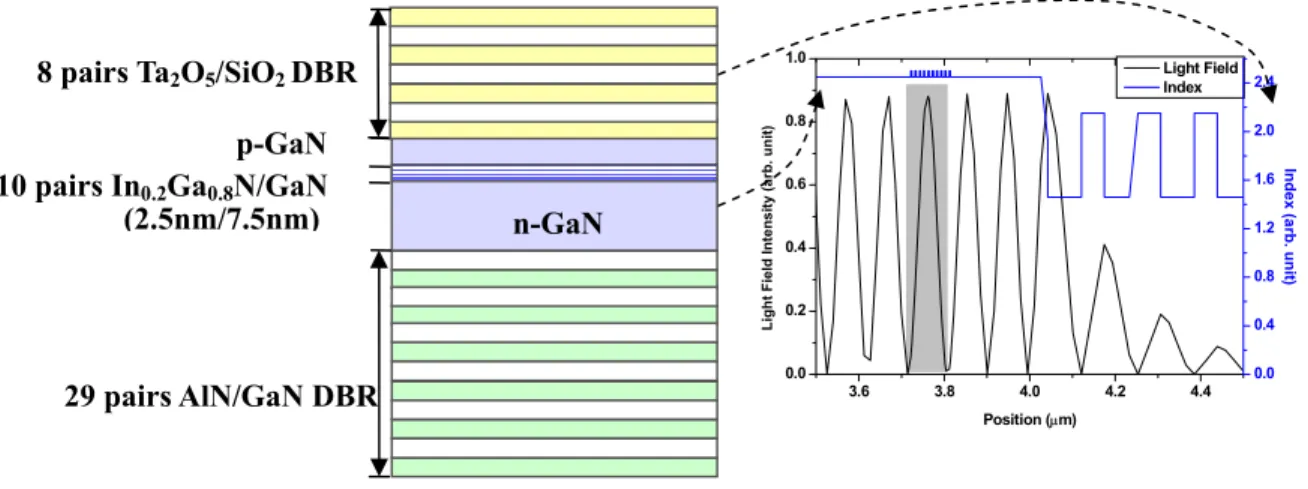
The hybrid DBR VCSELs were first grown epitaxially by a low pressure metal organic chemical vapor deposition (MOCVD) system (EMCORE D75) on two-inch diameter (0001)-oriented sapphire substrates using trimethylgallium and trimethylaluminum as group III source materials and ammonia as the group V source material. Then, the growth process was as follows. The substrate was thermally cleaned in hydrogen ambient for 5 min at 1100oC, and then a 30 nm thick GaN nucleation layer was grown at 500oC. The growth temperature was raised up to 1100oC for the growth of 2-µm GaN buffer layer. Then the 29 pairs of AlN/GaN DBR with six AlN/GaN superlattice insertion layers were grown under the fixed chamber pressure of 100 Torr similar to the previous reported growth conditions [5]. In order to reduce the tensile strain between the AlN and GaN, we inserted one superlattice into each five DBR periods at first twenty pairs of DBR. Then the superlattice was inserted into each three DBR periods for the remaining nine pairs of DBR to reduce the tensile strain. The overall AlN/GaN DBRs has 29 pairs with six superlattice insertion layers. Then the n-type GaN cladding layer and a ten pairs In0.2Ga0.8N/GaN (2.5 nm/10 nm) MQWs and p-type GaN cladding layer were grown to form a 5λ cavity in optical thickness for center wavelength of 460 nm. Finally, an eight pairs of Ta2O5/SiO2 dielectric mirror were deposited by electronic beam evaporation as the top DBR reflector to form the hybrid microcavity. The whole structure is schematically shown in Fig. 1. The hybrid DBR VCSEL samples with the completed layer structure were then sent for the optical characterization. The detailed laser properties will be given in the following sections. One test sample of 29 pairs of AlN/GaN DBR with six AlN/GaN superlattice insertion layers was also grown to measure the reflectivity using an n & k ultraviolet-visible spectrometer with normal incidence at room temperature, and to check the surface morphology using atomic force microscope (AFM). The average roughness measured was about 3.5 nm over a 5×5 µm2 surface area with crack-free surface morphology. The peak reflectivity of 99.4% at 461 nm with flat-topped stopband of 21 nm was measured, which is in agreement with the designed wavelength. Fig. 2 shows the room temperature reflectivity spectrum of whole microcavity under near normal incidence. The peak reflective is about 97 % with a large stopband of 70 nm resulted from the large refractive index contrast between Ta2O5 and SiO2 layers. Fig. 2 also shows the PL emission spectrum of the microcavity at room temperature pumped by the He-Cd laser at 325 nm for obtaining the quality factor Q of the fabricated microcavity. The cavity resonance mode at 464.2 nm with a FWHM of
0.61 nm is clearly observed. The cavity mode dip is located at reflectivity curve corresponding to the emission peak. This indicates that the InGaN/GaN MQWs emission peak was well aligned with the hybrid microcavity. The cavity Q factor was estimated from the
λ
∆
λ
to be about 760. This Q factor value agrees with the value calculated from the reflectivities of both AlN/GaN and Ta2O5/SiO2 DBRs.Fig. 1 Layer structure and the simulated standing wave patterns inside the cavity for the hybrid DBR VCSEL structure.
Fig. 2 Reflectivity and the PL spectra of microcavity at the room temperature.
2.2 Dielectric DBR VCSEL
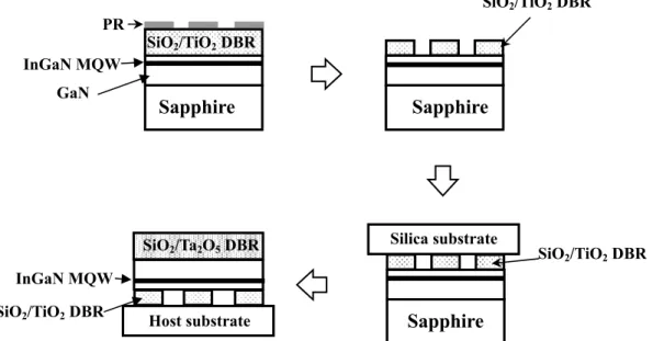
The schematic fabrication steps for dielectric DBR VCSEL are shown in Fig. 3. First, the layers structure of the GaN-based cavity, grown on a (0001)-oriented sapphire substrate by MOCVD is described as followed: a 30-nm nucleation layer, a 4-µm GaN bulk layer, MQWs consisting of 10 periods of 5-nm GaN barriers and 3-nm In0.1Ga0.9N
3.6 3.8 4.0 4.2 4.4 0.0 0.2 0.4 0.6 0.8 1.0 Light Field Index Position (µm) L igh t F iel d In te ns it y ( a rb . un it ) 0.0 0.4 0.8 1.2 1.6 2.0 2.4 Index (a rb. unit ) 10 pairs In0.2Ga0.8N/GaN 29 pairs AlN/GaN DBR n-GaN p-GaN (2.5nm/7.5nm) 8 pairs Ta2O5/SiO2 DBR 350 400 450 500 550 0.0 8.0k 16.0k 0 20 40 60 80 100
Intensity (a
.u
.)
Wavelength (nm)
0.61 nm
Reflectivity (%)
wells, and a 200-nm GaN cap layer. The peak emission wavelength of the MQWs for the as-grown sample was obtained to be 416 nm. Then, the dielectric DBR consisting of 6 pairs of SiO2 and TiO2 was evaporated on the top of GaN-based cavity. The stop band center of the DBR was tuned to 450 nm. The reflectivity of the SiO2/TiO2 DBR at 414 nm is obtained to be 99.5%. Next, in order to enhance the adhesion between the epitaxial layers and silica substrate, an array of disk-like patterns with the diameter of 60 µm was formed by standard photolithography process and the SiO2/TiO2 DBR mesas were formed by the buffer oxide etcher. The wafer was then mounted onto a silica substrate, which is nearly transparent to the wavelength of the excitation light and the VCSEL. A KrF excimer laser radiation at 248 nm was guided into the sample from back side of the sapphire to separate the sapphire from the epitaxial layers [6].
Fig. 3 Schematic process steps of the dielectric DBR VCSELs incorporating with two dielectric DBRs fabricated by the laser lift-off technique.
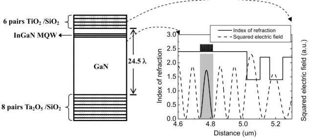
After the laser lift-off process, the sample was dipped into the H2SO4 solution to remove the residual Ga on the exposed GaN buffer layers. In the next step, the sample was lapped and polished by diamond powders to smooth the GaN surface since the laser lift-off process left a roughened surface. The mean surface roughness of the polished GaN surface measured by the atomic force microscopy (AFM) is about 1 nm over a scanned area of 20×20 µm2. However, to prevent the possible damage of the quality in MQWs during the lapping process, the 4-µm GaN bulk layer was preserved. Finally, the second DBR consisting of 8 pairs of SiO2 and Ta2O5 was deposited on the top of the polished GaN surface. The reflectivity of the SiO2/Ta2O5 DBR at 414 nm is 97%. The stop band center of the DBR was also tuned to 450 nm. The detailed layer structure of the VCSEL and the simulated electric field distribution in the cavity is shown in Fig. 4. The thickness of the whole epitaxial cavity was equivalent to the optical thickness of 24.5 emission wavelength. The optical thickness of the MQWs covered nearly half of the emission wavelength right between two adjacent nodes. Then, the laser emission characteristics of the completed dielectric DBR VCSELs were investigated by the optically pumped scheme.
Sapphire
InGaN MQW PR SiO2/TiO2 DBRSapphire
Silica substrateSapphire
Host substrate InGaN MQW SiO2/Ta2O5 DBR GaN SiO2/TiO2DBR SiO2/TiO2 DBR SiO2/TiO2 DBR3. RESULTS AND DISCUSSION
The emission spectrum of the GaN-based VCSEL structure was measured using a microscopy system (WITec, alpha snom) at room temperature. The optical pumping of the samples was performed using a frequency-tripled Nd:YVO4 355-nm pulsed laser with a pulse width of ~ 0.5 ns at a repetition rate of 1 KHz. The pumping laser beam with a spot size ranging from 30 µm to 60 µm was incident normal to the VCSEL sample surface. The light emission from the VCSEL sample was collected using an imaging optic into a spectrometer/CCD (Jobin-Yvon Triax 320 Spectrometer) with a spectral resolution of ~0.1 nm for spectral output measurement. The characteristic temperature of GaN VCSEL sample was measured using the same microscopic optical pumping system with the sample placed in a cryogenics controlled chamber. The temperature of the chamber can be controlled from room temperature of 300 K down to 60K using liquid nitrogen. The chamber has a window for laser pumping and output monitoring during the experiment. One polarizer was placed before the entrance of the monochromator to investigate the degree of polarization of the laser emission.
Fig. 4 Layer structure and the simulated standing wave patterns inside the cavity for the dielectric DBR VCSEL.
3.1 Characteristics of Hybrid DBR VCSEL
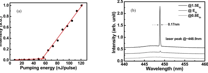
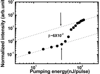
The light emission intensity from GaN-based VCSEL as a function of the pumping energy is shown in Fig. 5(a). A distinct threshold characteristic was observed at the threshold pumping energy (Eth) of about 55 nJ corresponding to an energy density of 7.8 mJ/cm2. Then the laser output increased linearly with the pumping energy beyond the threshold. A dominant laser emission line at 448.9 nm appearing above the threshold pumping energy is shown in the Fig. 5(b). The lower threshold density of this hybrid DBR VCSEL in comparison to our previous report [7] should be due to the improvement of the reflectivity of the epitaxially grown AlN/GaN DBR inserted with superlattice layers. The laser emission spectral linewidth reduces as the pumping energy above the threshold energy and approaches 0.17 nm at the pumping energy of 1.5Eth. In order to understand the spontaneous coupling factor β of this cavity, we normalized the
InGaN MQW 6 pairs TiO2 /SiO2
24.5 λ
8 pairs Ta2O5 /SiO2
GaN 4.6 4.8 5.0 5.2 0.0 0.5 1.0 1.5 2.0 2.5 3.0 Sq ua re d el ectric fiel d (a .u .) In de x of refrac tion Distance (um) Index of refraction Squared electric field
vertical scale of Fig. 5(a) and re-plotted it in a logarithm scale as shown in Fig. 6. According to the reference [8], the difference between the heights of the emission intensities before and after the threshold corresponds roughly to the value of β. The β value of our VCSEL estimated from Fig. 6 is about 6×10⁻². We also estimated the β value based on the
approximation equation used in reference [9]: 2 3
)
/
/(
4
3
n
V
Q
F
c p=
π
λ
, and p pF
F
+
=
1
β
, where Fp is the Purcellfactor, Q is the cavity quality factor, λ is the laser wavelength, Vc is the optical volume of laser emission, and n is the refractive index. Since the photoluminescence spectrum of our hybrid DBR VCSEL showed a narrow emission peak with full width at half maximum of 0.61 nm, cavity quality factor was estimated to be 760. The refractive index is 2.45 for the GaN cavity. For the estimation of the optical volume, we used the spot size of the laser emission image we reported previously [7] which was about 3 µm and the cavity length of about 9.5λ with considering the penetration depth of the DBRs. By using these parameters, the Purcell factor of about 2.9×10⁻² was obtained and we estimated the β value to be about 2.8×10⁻², which has the same order of magnitude as the above β value estimated from Fig. 6. This β value is three order of magnitude higher than that of the typical edge emitting semiconductor lasers (normally about 10-5) indicating the enhancement of the spontaneous emission into a lasing mode by the high quality factor microcavity effect in the VCSEL structure.
Fig. 5 (a) Laser emission intensity as a function of the pumping energy at room temperature conditions for hybrid DBR VCSEL; (b) The variation of laser emission spectrum with the increasing pumping energy for the hybrid DBR VCSEL.
The laser emission wavelength is 448.9nm with a linewidth of about 0.17 nm.
Figure 7 shows the laser emission intensity as a function of the angle of the polarizer at the pumping energy of 1.5Eth. The variation of the laser emission intensity with the angle of the polarizer shows nearly a cosine square variation. The degree of polarization (P) is defined as
min max min max
I
I
I
I
P
+
−
=
, where Imax and Imin are the maximum and minimum intensity0 20 40 60 80 100 120 0.0 0.2 0.4 0.6 0.8 1.0 In te n sit y (a .u .)
Pumping energy (nJ/pulse) 440 445 450 455 460
0.0 0.5 1.0 1.5 2.0 2.5 laser peak @~448.9nm 0.17nm In te n sit y (a rb . u n it) Wavelength (nm) @1.5Eth @ Eth @0.8Eth (a) (b)
of the nearly cosine square variation, respectively. The result shows that the laser beam has a degree of polarization of about 89%, suggesting a near linear polarization property of the laser emission. The relationship between the threshold energy and the operation temperature could be characterized by the equation Eth=E0×
e
T/ T0, where T0 is the characteristictemperature and E0 is a constant. Therefore, we obtain a high characteristic temperature of about 244 K by linear fitting
the experiment data, which the threshold energy gradually increased as the operation temperature rose from 120 K to 300 K. This T0 value is close to the T0 value of 300 K for GaN-based VCSELs predicted by Iga et al. [10], and higher than
the reported T0 of 170 K [11] or 235 K [12] for the GaN-based edge-emitting laser diode.The high To of our sample
could be due to various factors. We measured the lasing wavelength variation with the temperature. The result showed a slight red shift of about 1.6 nm as the temperature rose from 120K to 300K. The PL emission of the MQW was also measured and the result showed a red shift of about 2.9 nm over the same temperature range. These results suggest that the gain peak almost align with the cavity mode within this temperature variation range. Therefore the high characteristics temperature obtained from our GaN VCSEL sample could be partly attributed to the good alignment of the gain peak and cavity mode. Furthermore the ten-pair In0.2Ga0.8N/GaN MQW structure could help to suppress the carrier leakage from the MQW active layers to the cladding layers.
Fig. 6 Laser emission intensity versus pumping energy in logarithmic scale for hybrid DBR VCSEL.
3.2 Characteristics of Dielectric DBR VCSEL
Figure 8(a) shows the laser emission intensity from the dielectric DBR VCSEL as a function of the pumping energy at room temperature conditions. A clear evidence of threshold condition occurred at the pumping energy of Eth = 270 nJ corresponding to an energy density of 21.5 mJ/cm2. The output laser intensity from the sample increased linearly with the pumping energy level beyond the threshold energy. The estimated carrier density at the threshold is in the order of 1020 cm-3 assuming that the pumping light with the emission wavelength of 355 nm has experienced a 60% transmission through the SiO2/Ta2O5 DBR layers and undergone a 98% absorption in the thick GaN layer. According to the report by
101 102 10-1 100 101 102 103 β~6X10⁻²
N
o
rm
alize
d
in
te
n
sity
(a
rb
.u
n
it)
Pumping energy(nJ/pulse)
Park [13], the gain coefficient of InGaN at this carrier density level is about 104 cm-1. We estimated the threshold gain (gth) value of our VCSEL using the equation gth ≥ 1/(ξLa) × ln(1/R1R2), where ξ is the axial enhancement factor, La is the
total thickness of the InGaN MQWs and R1 and R2 are the reflectivity of the dielectric DBRs. Since the active region
covers half of the emission wavelength, ξ is unity. We obtained an estimated gain coefficient of about 104 cm-1 which is consistent with the above gth value estimated from the carrier density. This also proved that the quality of the MQWs had
been kept after the laser lift-off and lapping process. Figure 8(b) shows the evolution of the VCSEL emission spectrum with the pumping energy at room temperature. When the pumping energy is below the threshold, the spontaneous emission spectrum shows multiple cavity modes. The mode spacing is about 7 nm corresponding to a cavity length of 4.3 µm, which is nearly equal to the thickness of the epitaxial cavity. The linewidth of a single cavity mode is 0.8 nm as shown in the inset of Fig. 8(b). The cavity quality factor (Q factor) estimated from the linewidth is about 518. Considering the optical absorption of GaN layer, an estimated effective cavity reflectivity based on this Q factor is about 97%, which is close to the cavity reflectivity formed by the two dielectric DBRs. This result indicates the laser cavity structure was nearly intact after the laser lift-off process. As the pumping energy increased above the threshold, a dominant laser emission line appeared at 414 nm with a narrow linewidth of about 0.25 nm. The lasing wavelength is located at one of cavity modes near the peak emission wavelength of the InGaN MQWs.
Fig. 7 The polarization characteristic of the laser emission at the pumping energy of 1.5Eth for the hybrid DBR VCSEL. The solid dot shows the experiment data and the solid line is the fitting curve.
The laser emission polarization contrast between two orthogonal directions was measured. The difference between the two angles of minimum intensities is 180o and a degree of polarization of about 70% is estimated. The lower degree of polarization in comparison to the hybrid DBR VCSEL could be due to the smaller Q factor for this dielectric DBR VCSEL. The spontaneous coupling factor β was estimated as about 1.1x10⁻². Since the cavity volume of this dielectric DBR VCSEL is large than the above hybrid DBR VCSEL, the Purcell factor and the spontaneous coupling factor β shall be lower accordingly. The threshold pumping energy increased gradually with increasing temperature. We obtain a
-100 -50 0 50 100 0.0 0.2 0.4 0.6 0.8 1.0
Imax~17.7Imin
experiment data N o rm alize d In te n sit y (a rb .u n it)
Angle of Polarizer (degree)
-100 -50 0 50 100
characteristic temperature of about 278 K for this dielectric type VCSEL for the temperature range of 58 to 322 K by linearly fitting the experimental result. This T0 value is close to the T0 value for the hybrid DBR VCSEL, showing that
the potential of high temperature operation in GaN VCSELs.
Fig. 8 (a) Laser emission intensity as a function of the pumping energy at room temperature conditions for the dielectric DBR VCSEL.; (b) Emission spectra from the dielectric DBR VCSEL at various pumping energy. The lasing emission
wavelength is 414 nm with a linewidth of 0.25 nm. The inset shows the rescaled emission spectrum under pumping power of 0.25 Eth
4. ELECTRICALLY DRIVEN GAN VCSELS
Based on a hybrid DBR configuration, we will briefly report the fabrication of a high Q (~895) vertical cavity device comprising a high-reflectivity AlN/GaN DBR, an InGaN/GaN active region, an Indium-tin-oxide (ITO) transparent current-spreading layer and a Ta2O5/SiO2 DBR, and we observe a very narrow linewidth emission. Figure 9 shows a schematic diagram of the overall device structure. The sample was grown by a metal-organic chemical vapor deposition system on a polished optical-grade c-face (0001) 2’’ diameter sapphire substrate. Following the growth of a GaN buffer layer, a 25-pair AlN/GaN DBR was deposited and in-situ monitored at a fixed wavelength of 460 nm. Finally, a 3-λ optical thickness (λ = 460 nm) active pn-junction region, composed of ten In0.2Ga0.8N(3 nm) / GaN(6 nm) multiple quantum wells, a 380 nm-thick Si-doped n-type GaN and a 100 nm-thick Mg-doped p-type GaN layers, were grown atop the GaN/AlN DBR. A sample with only a 25-pair AlN/GaN DBR was also grown for reflectivity measurement. A peak reflectivity of 98% was measured, with a spectral width of the maximum reflectance band ~ 25nm. The process of device began with the deposition of a 0.3 µm-thick SiNx etching mask by plasma enhanced chemical vapor deposition and the definition of mesa region by photo-lithography. The mesa etching was then performed with Cl2/Ar as the etching gas in an inductively coupled plasma reactive ion etching (ICP-RIE) system with the ICP power and bias power operated at 13.56 MHz. After removing the etching mask, we re-deposited and patterned a 0.2 µm-thick SiNx layer to define a
390 395 400 405 410 415 420 425 430 435 440 E m is si o n in te n sity (a .u .) Wavelength (nm) 400 405 410 415 420 425 E=0.25Eth Intensity (a. u .) Wavelength (nm) 1.13 Eth 0.25 Eth Eth FWHM~0.25 nm 100 150 200 250 300 350 0 10 20 30 40 50 E m issio n in ten sit y ( a.u .)
5-30gm
ITO current-spreading layer C
)
/ 8-pair Ta105!Si01 DBR25-pair AIN/GaN DBR Sapphire
Ni/Au p-contact
SiNx
Ti/Al/Ni/Au n-contact
current aperture of 50 µm in diameter. Then, a 240 nm-thick layer of ITO corresponding to one λ optical thickness was deposited onto the current aperture region using an e-gun. The ITO was employed as a p-type ohmic contact material and annealed at 525oC for ten minutes under nitrogen ambient to reduce the contact resistance and increase transparency. Over 98% of transmittance was obtained at λ = 460 nm after annealing. The metal contact layers were then patterned by a lift-off procedure and deposited onto samples by electron beam evaporation. Ti/Al/Ni/Au (20/150/20/150 nm) and Ni/Au (20/150 nm) served as the n-type electrode and p-type electrode, respectively. A 30-µm emission aperture was formed by lifting off the p-type metal atop the ITO layer. Finally, an 8-pair Ta2O5/SiO2 DBR (measured reflectivity over 99% at λ = 460 nm) was evaporated as the top mirror to complete the device process.
Fig. 9 A schematic diagram of the overall vertical cavity light emitter structure.
Fig. 10 The emission spectrum of the vertical cavity light emitter operating at three different currents, 3 mA, 6 mA, and 10 mA.
450
455
460
465
470
475
480
In
te
n
sity
(
arb
. u
n
it)
Wavelength (nm)
@ 10mA @ 6mA @ 3mAThe characteristics of the fabricated device were performed by using a probe station and driven by a Keithley 238 CW current source. The emission light was then collected by a 25 µm diameter multimode fiber using a microscope with a 40X objective and fed into the spectrometer with a spectral resolution of 0.15 nm. Figure 10 shows the emission spectrum of the device operating at three different current, 3 mA, 6 mA, and 10 mA. As the injection current was increased, a single emission peak at 465.3 nm became dominant with rapidly increasing intensity and narrowing linewidth. The full width at half maximum of the emission linewidth decreased from 0.57 nm to 0.52 nm as the driving current was increased to 10 mA, which is, to our best knowledge, the narrowest linewidth recorded for GaN-based vertical cavity light emitter. From the emission peak wavelength at λ = 465.3 nm and the emission linewidth ∆λ = 0.52 nm, the cavity Q is estimated by λ/∆λ to be ranging from 816 to 895. Since the cavity Q formed by our vertical cavity with both high reflectivity DBRs (R = 98% and 99%) and ITO current spreading layer was calculated to be about 890 without taking into account the absorption in the InGaN/GaN pn-junction region, the narrowing linewidth observed represents that the active region was approaching the transparency condition before lasing. In comparisons to conventional LEDs with a spectral linewidth of about 20 nm, our high-Q vertical light emitter has demonstrated a rather coherent emission.
5. CONCLUSION
We have reported fabrication technology of two types of GaN-based VCSEL structures: hybrid DBR VCSELs and dielectric DBR VCSELs with similar InGaN/GaN MQW active layer. For the hybrid DBR VCSEL, we have fabricated a crack-free, high reflectivity AlN/GaN DBR by insertion of superlattice layers and use the high reflective Ta2O5/SiO2 as dielectric mirror and achieved laser operation under optical pumping at room temperature. The laser has a threshold energy of 55 nJ and emission wavelength at 448.9 nm with a linewidth of 0.17 nm. The laser emission showed a high degree of polarization of 89% and high spontaneous emission coupling factor of 6×10⁻². For the dielectric DBR VCSEL, a key fabrication technique, laser lift-off was used for formation of dielectric DBR cavity. The dielectric DBR VCSEL also achieved laser action under optical pumping at room temperature condition. The laser has a threshold pumping energy of 270 nJ and emitted wavelength at 414 nm with a linewidth of 0.25 nm. The laser also has degree of polarization of 70%. From the primary results of the GaN vertical cavity light emitter, the possibility of a GaN-based VCSEL could be realized by future optimization of higher DBR reflectivities and ITO transparency, lower resistive heating and better lateral mode confinement.
6. ACKNOWLEDGMENT
The authors would like to acknowledge Prof. K. Iga of Tokyo Institute of Technology for helpful suggestion. The work was supported by the MOE ATU program and the National Science Council under contract nos. NSC 95-2120-M-009-008, NSC 95-2752-E-009-007-PAE, and NSC 95-2221-E-009-282.
REFERENCES
1. Joan M. Redwing David A. S. Loeber and Neal G. Anderson Michael A. Tischler and Jeffrey S. Flynn, Appl. Phys. Lett., 69, 1, (1996)
2. Takao Someya, Koichi Tachibana, Jungkeun Lee, Takeshi Kamiya and Yasuhiko Arakawa, Jpn. J. Appl. Phys., 37, L1424, (1998)
3. Y.-K. Song, H. Zhou, M. Diagne, I. Ozden, A Vertikov, A. V. Nurmikko C. Carter-Coman, R. S. Kern, F. A. Kish, and M. R. Krames, Appl. Phys. Lett., 74, 3441, (1999)
4. J.-F. Carlin, J. Dorsaz, E. Feltin, R. Butté, N. Grandjean, M. Ilegems, and M. Laügt, Appl. Phys. Lett. 86, 031107, (2005)
5. G.S. Huang, T. C. Lu, H. H. Yao, H.C. Kuo, S. C. Wang, Chih-wei Lin and Li Chang, Appl. Phys. Lett., 88, 061904, ( 2006)
6. W. S. Wong, T. Sands, N. W. Cheung, M. Kneissl, D. P. Bour, P. Mei, L. T. Romano and N. M. Johnson, Appl. Phys. Lett. 75, 1360 (1999).
7. Chih-Chiang Kao, Y. C. Peng, H. H. Yao, J. Y. Tsai, Y. H. Chang, J. T. Chu, H. W. Huang, T. T. Kao, T. C. Lu, H. C. Kuo and S. C. Wang, Appl. Phys. Lett., 87, 081105, (2005)
8. R. J. Horowicz, H. Heitmann, Y. Kadota and Y. Yamamoto, Appl. Phys. Lett, 61, 393 (1992) 9. S. Kako, T. Someya, and Y. Arakawa, Appl. Phys. Lett., 80, 722 (2002)
10. T. Honda, H. Kawanishi, T. Sakaguchi, F. Koyama and K. Iga, MRS Internet. Nitride Semicond. Res. 4S1 G6.2 (1999.)
11. C. Skierbiszewski, P. Perlin, I. Grzegory, Z. R. Wasilewski, M. Siekacz1, A. Feduniewicz, P. Wisniewski, J. Borysiuk1, P. Prystawko, G. Kamler1, T. Suski1 and S. Porowski, Semicond. Sci. Technol., 20, pp. 809-, (2005.) 12. M. Ikeda and S. Uchida, Phys. Stat. Sol. (a), 194, no. 2, pp. 407-413, (2002)